• Journal of Semiconductors
  • Vol. 41, Issue 5, 051205 (2020)
Gang Cao1、2, Chuantong Cheng1, Hengjie Zhang1, Huan Zhang1, Run Chen1, Beiju Huang1, Xiaobing Yan2, Weihua Pei1, and Hongda Chen1、3
Author Affiliations
  • 1State Key Laboratory on Integrated Optoelectronics, Institute of Semiconductors, Chinese Academy of Sciences, Beijing 100083, China
  • 2National–Local Joint Engineering Laboratory of New Energy Photovoltaic Devices, Key Laboratory of Digital Medical Engineering of Hebei Province, College of Electron and Information Engineering, Hebei University, Baoding 071002, China
  • 3College of Materials Science and Opto-Electronic Technology, University of Chinese Academy of Sciences, Beijing 100049, China
  • show less
    DOI: 10.1088/1674-4926/41/5/051205 Cite this Article
    Gang Cao, Chuantong Cheng, Hengjie Zhang, Huan Zhang, Run Chen, Beiju Huang, Xiaobing Yan, Weihua Pei, Hongda Chen. The application of halide perovskites in memristors[J]. Journal of Semiconductors, 2020, 41(5): 051205 Copy Citation Text show less

    Abstract

    New neuromorphic architectures and memory technologies with low power consumption, scalability and high-speed are in the spotlight due to the von Neumann bottleneck and limitations of Moore's law. The memristor, a two-terminal synaptic device, shows powerful capabilities in neuromorphic computing and information storage applications. Active materials with high defect migration speed and low defect migration barrier are highly promising for high-performance memristors. Halide perovskite (HP) materials with point defects (such as gaps, vacancies, and inversions) have strong application potential in memristors. In this article, we review recent advances on HP memristors with exceptional performances. First, the working mechanisms of memristors are described. Then, the structures and properties of HPs are explained. Both electrical and photonic HP-based memristors are overviewed and discussed. Different fabrication methods of HP memristor devices and arrays are described and compared. Finally, the challenges in integrating HP memristors with complementary metal oxide semiconductors (CMOS) are briefly discussed. This review can assist in developing HP memristors for the next-generation information technology.

    1. Introduction

    Because of the rapid developments in information technologies, massive amounts of data need to be efficiently stored and processed. However, the traditional computing hardware and memories have been approaching their limits under the current technologies. The human brain shows an absolute advantage over modern computers due to its highly parallel computation and ultralow power consumption[1]. Synaptic plasticity is essential for learning and memory[2]. The memristor (short for memory resistor) is a two-terminal circuit element characterized by a pinched hysteresis loop in the I–V plane and plastic resistance[3]. Hence, the memristor can work as an artificial synapse and offers novel applications in neuromorphic computing[4, 5], information storage[6], and hardware security[7].

    To date, various materials have been utilized to fabricate memristors, including metal oxides[8, 9], organics[10], chalcogenides[11], and especially halide perovskites (HP)[12-14]. In the past few years, metal HP materials have become a game-changer in the photovoltaic industry due to its remarkable properties[15, 16], such as high optical absorption coefficients, high charge carrier mobility, adjustable direct optical band gap and so on[17-22]. HP has also been successfully used in light emitting diodes[23], field effect transistors[24], and photodetectors[25]. And HPs are well-suited for memristor applications because their mixed ion–electron conduction behavior allows halide counterions to move under applied optical, electric, or thermal fields[26, 27].

    This review is organized as follows: Section 2 gives a brief definition and working principles of memristors. Section 3 gives a brief introduction to HPs. In Section 4, recent advances in HP memristors are reviewed. In Section 5, the fabrication methods of HP-based memristors devices and arrays are reviewed. Finally, some challenges and perspectives for the development of HP-based memristors are presented in Section 6.

    2. Memristors

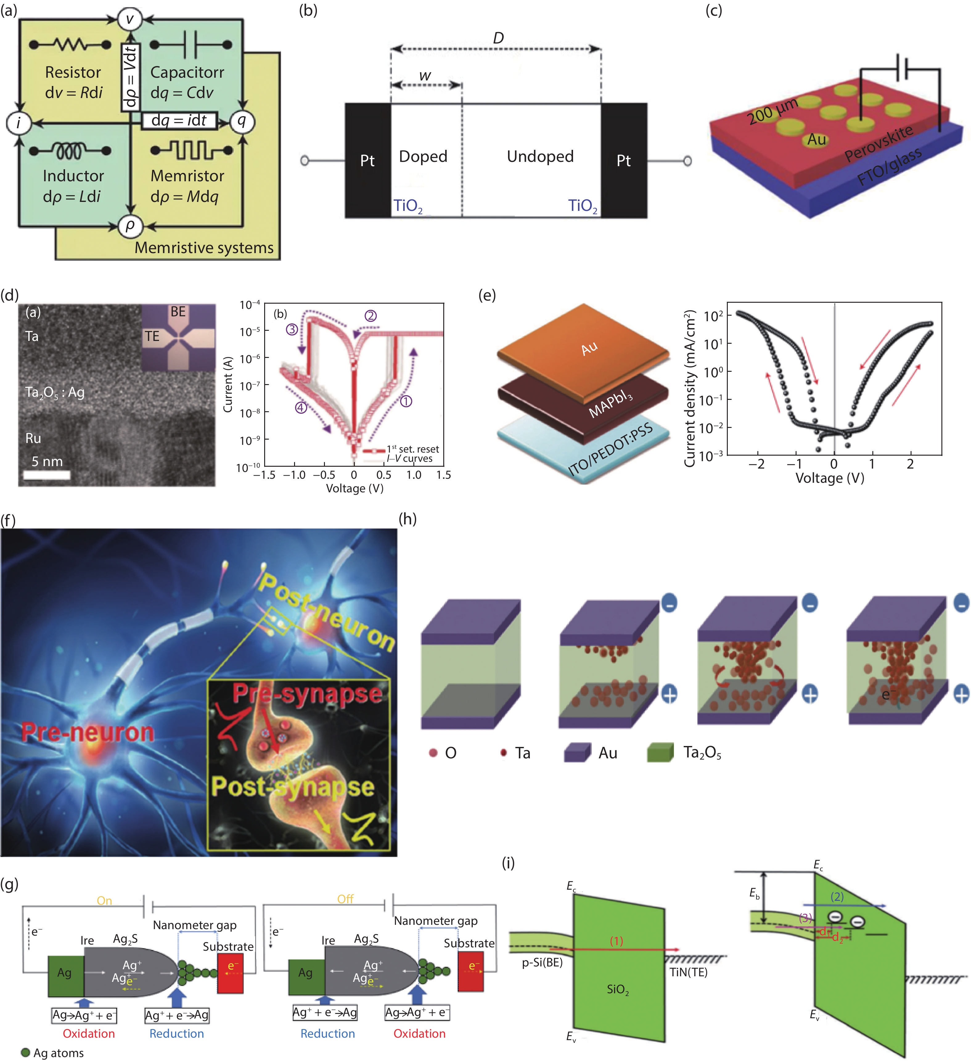
    Memristor is considered to be the fourth basic circuit element in addition to resistor, capacitor, and inductor. The concept was proposed by Chua in 1971. It is a circuit device with a relationship between magnetic flux and charge, as shown in Fig. 1(a)[28]. Due to the lack of experimental evidence, related theories have not attracted much attention in the past decades until Strukov et al. successfully produced the Pt/TiO2/Pt device structure with memristive performance, as shown in Fig. 1(b)[29]. In previous reports and studies, most memristor structures use the sandwich structure as shown in Fig. 1(c)[14] in which the metal is used as the bottom electrode (BE) and top electrode (TE), and functional layers consist of insulators, semiconductors, organics, or perovskites. Such a simple device structure enables the large-scale integration of memristors in high-density crossbar switch arrays.

    (Color online) (a) Four basic circuit elements: resistor, capacitor, inductor and memristor. Reprinted from Ref. [28]. (b) The variable resistance model of memristor proposed by Strukov et al. Reprinted from Ref. [29]. (c) Schematic diagram of a typical sandwich structure memristor of Au/MAPbI3−xClx/ITO. Reprinted from Ref. [14]. (d) Ta/Ta2O5:Ag/Ru high resolution transmission electron microscope (HRTEM) image and typical abrupt I–V curve. Reprinted from Ref. [30]. (e) Schematic of vertical structure Au/MAPbI3/PEDOT:PSS/ITO and dark current of memristor. Reprinted from Ref. [32]. (f) Schematic diagram of synaptic working principle. Reprinted from Ref. [35]. (g) Diagram of atomic switches in ON and OFF states via ECM mechanism. Reprinted from Ref. [44]. (h) Schematic diagram of VCM-induced resistance switching behavior. Reprinted from Ref. [45]. (i) Schematic diagram of Schottky barrier for TiN/SiO2/Si structure. Reprinted from Ref. [53].

    Figure 1.(Color online) (a) Four basic circuit elements: resistor, capacitor, inductor and memristor. Reprinted from Ref. [28]. (b) The variable resistance model of memristor proposed by Strukov et al. Reprinted from Ref. [29]. (c) Schematic diagram of a typical sandwich structure memristor of Au/MAPbI3−xClx/ITO. Reprinted from Ref. [14]. (d) Ta/Ta2O5:Ag/Ru high resolution transmission electron microscope (HRTEM) image and typical abrupt I–V curve. Reprinted from Ref. [30]. (e) Schematic of vertical structure Au/MAPbI3/PEDOT:PSS/ITO and dark current of memristor. Reprinted from Ref. [32]. (f) Schematic diagram of synaptic working principle. Reprinted from Ref. [35]. (g) Diagram of atomic switches in ON and OFF states via ECM mechanism. Reprinted from Ref. [44]. (h) Schematic diagram of VCM-induced resistance switching behavior. Reprinted from Ref. [45]. (i) Schematic diagram of Schottky barrier for TiN/SiO2/Si structure. Reprinted from Ref. [53].

    Memristor devices can demonstrate different memristive characteristics according to different mechanisms by applying an external electric field, which can be divided into abrupt changes (Fig. 1(d)) and gradual changes (Fig. 1(e))[30-32]. The resistive switching (RS) of the abrupt memristor (also called resistive random-access memory (RRAM)) is discrete, also known as a digital memristor. This type of memristor has multiple resistance states and can be developed for information storage and logic applications, where the stored information consists of different resistance states (high resistance state (HRS) and low resistance state (LRS))[33, 34]. The indicators for measuring RRAM include threshold voltage distribution, RHRS/RLRS ratio, retention, durability, and power consumption. The resistance of the memristor with gradual changes is continuous, also known as the analog memristor. The conductance of this type of memristor is continuously adjustable; thus, it behaves similarly to progressively continuous adjustable synaptic weights in biological synapses. The human brain contains about 1015 synapses. The information transferred in the neuron network is assisted by the biological synapses (See Fig. 1(f)), which adjust the connection strength between two neurons via neurotransmitters flux. The synaptic plasticity is considered as the basis of brain's learning and memory functions. Scientists have discovered that memristors can simulate biological synaptic functions, including spiking-time-dependent plasticity (STDP), paired-pulse facilitation (PPF), excitatory postsynaptic current (EPSC), short-term plasticity (STP), long-term plasticity (LTP), learning, and forgetting[36-39]. These bionic functions have opened up excellent prospects for memristors to implement neuromorphic computing systems, and can gradually develop into higher-order learning and associative memory functions[8, 40].

    To understand the memristive characteristics of a memristor, it is necessary to study its mechanism. Firstly, the physical mechanism of the memristor is introduced in detail. There are two main types of physical mechanisms: formation and rupture of conductive filaments (CF) and interface types[41-43]. The formation and rupture of CF are mainly caused by ion migration and redox reactions inside the material under the external electric field. According to the type of mobile ions, the RS can be divided into electrochemical metallization (ECM) (Fig. 1(g))[44] and valence change mechanism (VCM) (Fig. 1(h))[45]. Memristors operated by ECM usually use active metals as the TE (such as Ag and Cu). The migration of active metal ions is a key factor causing RS[46, 47]. When a positive voltage is applied to the TE of the device, the active metal is oxidized to cations. These cations continue to diffuse downward, passing through the functional layer under the drive of a positive electric field. Finally, the ions are reduced to metal at the BE, forming CF. The continuous growth of CF facilitates the communication between the TE and BE, and the memristor switches from HRS to LRS. In contrast, when a negative voltage is applied, the memristor switches from LRS to HRS. Selecting a functional layer material with excellent performance can effectively control the formation and rupture of CF[48, 49]. Another type of RS is caused by VCM in which the memristor operates usually based on the migration and redistribution of anions, thereby changing the valence state of the functional layer material[45, 50]. To explain the RS behavior caused by VCM, we use metal oxide as a functional layer as an example to explain. When an electric field is applied, oxygen ions and oxygen vacancies (Vos) migrate. During the SET process (i.e., memristor switching from HRS to LRS), Vos accumulate towards the BE under the action of a positive electric field, resulting in the formation of CF of Vos. During the RESET process (memristor switching from LRS to HRS), Vos combine with oxygen ions, causing the CF to rupture[51, 52]. Moreover, another type of physical mechanism that is a uniform interface type physical mechanism (Fig. 1(i))[53], which is mainly caused by the Schottky barrier. The memristor functional layer typically uses an insulator to build a Schottky contact point between the insulator and the electrode. The change in the Schottky barrier is usually accompanied by charge trapping/detrapping or anion migration at the insulating layer near the electrode[54, 55]. Next, the conduction mechanism model of memristors is briefly introduced. The conductive mechanism of memristors usually uses some models to fit the I–V curve, such as space charge-limited conduction (SCLC, IV2), Schottky emission (ln IV1/2), Poole-Frenkel emission (ln (I/V) ∝ V)1/2, trapped assisted tunneling (TAT, ln J ∝ 1/E), thermionic emission (IV) and Fowler-Nordheim tunneling (FNT, ln (I/V2) ∝ 1/V)[56-59].

    3. Halide perovskites

    3.1. Structure

    Perovskite material is a compound with ABX3 crystal type[60], as shown in Fig. 2(a), generally having cubic or octahedral shape and excellent physical properties. A is a monovalent cation and can be an organic (methylammonium CH3NH3+) or inorganic (Cs+) cation. B is a divalent cation, such as Pb2+, Sn2+, and the like, and X is an anion. When X is oxygen (O), it is called an oxide perovskite, and when X is a halide (I or Br), it is called an HP[61]. In the past ten years, HPs have played an important role in solar cells and has become a hot topic due to its excellent optical and charge transport characteristics[62, 63]. HPs can be divided into inorganic HP and organic-inorganic halide perovskite (OHPs) according to different ions. Inorganic HPs (Fig. 2(b))[64] are a class of functional materials with perovskite structure composed of inorganic cations (alkaline earth metal cations), transition metals, and halogens. They possess an adjustable electronic structure and excellent photoelectric performance. In particular, its advantages of easy solution processing enable low cost and large-scale applications[15, 65]. Inorganic HPs have been applied to solar cells and light-emitting devices and memristors, and their challenges such as stability and heavy metal toxicity have been gradually resolved[66]. OHPs (Figs. 2(c)2(e))[67] have adjustable band gap (ABG), high efficiency, strong light absorption ability, and high crystallinity at low temperatures. Therefore, they have been widely used in photovoltaic applications, photodetectors, transistors, light-emitting diodes, and storage devices[68-70].

    (Color online) (a) Atomic structure diagram of perovskite. Reprinted from Ref. [60]. (b) Structure of CsPbBr3 nanocrystals. Reprinted from Ref. [64]. (c) Au/CH3NH3PbI3–xClx/FTO device structure chemical diagram and voltage application diagram. (d) Scanning electron microscope (SEM) image of the surface morphology of the CH3NH3PbI3–xClx film. (e) Cross-sectional SEM image of Au/CH3NH3PbI3–xClx/FTO. Reprinted from Ref. [67].

    Figure 2.(Color online) (a) Atomic structure diagram of perovskite. Reprinted from Ref. [60]. (b) Structure of CsPbBr3 nanocrystals. Reprinted from Ref. [64]. (c) Au/CH3NH3PbI3–xClx/FTO device structure chemical diagram and voltage application diagram. (d) Scanning electron microscope (SEM) image of the surface morphology of the CH3NH3PbI3–xClx film. (e) Cross-sectional SEM image of Au/CH3NH3PbI3–xClx/FTO. Reprinted from Ref. [67].

    3.2. Properties

    HPs have widely used active layer materials in the field of optoelectronics, such as light-emitting diodes, and photodetectors. In previous reports, HPs have become a hot topic in solar cell research because the power conversion efficiency has rapidly increased by more than 20%, and the precursors in solution have simple processability[71]. Moreover, since HPs exhibit light absorption and high carrier mobility, they exhibit good performance as photodetectors[69]. In recent years, HP materials have been demonstrated to have unique optoelectronic properties, such as high absorption coefficient[72], small exciton binding energy[72], long carrier diffusion length[17], excellent optoelectronic properties, high mobility[73], low defect density[20], and ABG[74]. It has been widely used as the functional layer in memristors and have shown excellent resistance-switching performance through tests[75].

    The HP material is usually expressed as ABX3, where A and B can be replaced by various elements so that the properties of HPs can be tailored, as shown in Fig. 3. Firstly, the most important characteristics of HPs are the ABG and variable structure. Xiao et al. reported an article on the structural stability and optical properties of CsPb2Br5 with a two-dimensional (2D) layer structure under high pressure[72]. The report showed that CsPb2Br5 microplates initially showed the narrowest band gap and then blue-shifted with pressure. The pentahedron pattern of Pb–Br bond length (out of Pb–Br inorganic layer) and Br–Pb–Br bond angle (perpendicular to the Pb–Br inorganic layer) in Pb–Br decreases linearly during the initial compression. After further compression, the Br–Pb–Br bond angle showed a significant inflection point at 1.65 GPa, which is consistent with the pressure point of isomorphic transformation. The results indicate that the band gap changes may be caused by orbital interactions related to the synergistic effect of pressure-induced changes in the Pb–Br pentahedron network, particularly the Pb–Br bond lengths and Br–Pb–Br bond angles[72]. Biswas et al. reported an article on the transition from direct band gap 3D CsPbBr3 nanocrystals to indirect band gap 2D CsPb2Br5 nanosheets, and the report also points to the origin of the luminescent properties of the material[76]. Biswas et al. used a single-pot solution conversion method to convert 3D CsPbBr3 nanocrystals into 2D CsPb2Br5 nanosheets. The high temperature and the presence of long-chain ammonium ligands help to destroy the 3D network of CsPbBr3 and reorganize into a 2D flat structure of CsPb2Br5 in the presence of excess PbBr2. However, the calculation of the electronic structure of CsPb2Br5 shows that it has an indirect band gap of 3.06 eV between VBM and CBM at point X and Γ, so it should not have light-emitting characteristics[76]. Through experiments and density functional theory calculations, the surface of CsPb2Br5 contains amorphous ammonium complexes of PbBr42− and Pb2Br5, which give the material its luminescent properties. Secondly, the characteristics of HPs are high carrier mobility and good light absorption. The ion migration hypothesis has long been verified by metal oxide perovskite materials, and nowadays, inorganic HPs have also demonstrated the presence of ion migration[77]. Tress et al. reported a metal halide perovskite (MHP) as a mixed electron ion conductor[71]. The article details the principle of mobile ion defects related to hysteresis. The defect ion migration is an essential feature of MHP in which halide vacancies (such as iodine vacancies) have been identified as the main mobile ion defect type related to hysteresis, and other mobile anions and cations can also be observed over a longer period[78]. In 2018, Loh et al. reported a 2D hybrid perovskite with tunable optoelectronic properties due to the reversible surface relaxation of the material[79]. Strip a 2D Ruddlesden-Popper perovskite (RPP) consisting of multiple organic/inorganic quantum wells into several layers. In the paper, a cm-sized pure single-phase RPP perovskite, (CH3(CH2)3NH3)2(CH3NH3)n−1PbnI3n+1 (n = 1–4) was synthesized. And a highly efficient photodetector was successfully prepared with a light gain of 105 using a thin molecular RPP crystal (n = 4)[79]. Finally, the HPs have ultra-high flexibility, low defect density. Shi et al. first reported a high-performance flexible lead-free 2D perovskite (PEA)2SnI4[80] in which, when 30 mol% SnF2 was added to the perovskite, the stability and repeatability of the device were significantly improved, making it suitable for flexible photoconductors and synaptic devices. Therefore, based on these excellent properties of HP, it is expected that HP materials will be used in a wider range of electronic devices in the near future.

    (Color online) Properties of halide perovskites. (a) Tunable bandgap. Reprinted from Ref. [72]. (b) Variable structure. Reprinted from Ref. [76]. (c) High carrier mobility. Reprinted from Ref. [71]. (d) Good light absorption. Reprinted from Ref. [79]. (e) Ultra-high flexibility. Reprinted from Ref. [80].

    Figure 3.(Color online) Properties of halide perovskites. (a) Tunable bandgap. Reprinted from Ref. [72]. (b) Variable structure. Reprinted from Ref. [76]. (c) High carrier mobility. Reprinted from Ref. [71]. (d) Good light absorption. Reprinted from Ref. [79]. (e) Ultra-high flexibility. Reprinted from Ref. [80].

    4. Halide perovskite memristors

    4.1. Electrical memristors

    Memristors are promising candidates for the establishment of synaptic devices in neuromorphic systems due to their strong expandability, simple structure, and fast switching speed. At the same time, they are expected to construct flexible and implantable artificial neuromorphic systems due to their excellent mechanical and biological characteristics[81-83]. With the continuous development of semiconductor technology, the trend of combining memristors with physical objects is increasing. The electrical characteristics of the memristor can be tested to determine whether the device has a good performance by applying a voltage to the memristor under the driving of the voltage. Choi et al. reported the first application of OHP materials (Au/CH3NH3PbI3−xClx/FTO) for non-volatile memory devices with significant RS effect[67]. The device exhibits bipolar RS performance with a switching voltage of less than 1 V, which has been reported for the first time. Sun et al. constructed a sandwich structure (ITO/PEDOT:PSS/CH3NH3PbI3/C)[84]. The device has an on/off ratio of approximately 104 at a read voltage of 50 mV, which is the best result obtained from an OHP-based memristor. Zou et al. selected electrochemically active metal electrodes and successfully prepared metal (Ag/Cu/Ti/Zn/Al)/CH3NH3PbClxI3−x/TiO2 compact layer/FTO memristor devices[85]. It has a switching current ratio as high as 1.9 × 10⁹, which is the highest value among all memristors reported so far. Such a high switching current ratio may result in faster read speeds, fewer errors, and lower power consumption.

    In electrical memristors, the most critical properties are switching speed, durability, retention, and power consumption. HP materials show excellent memristive properties, such as high Ron/Roff ratios and low switching voltages. In 2019, Park et al. reported a lead-free perovskite-based material (MA3Sb2Br9 (MA = CH3NH3)) for the resistive conversion of memristors and neuromorphic computing with low energy consumption[86]. In this paper, Ag/PMMA/MA3Sb2Br9/ITO devices are demonstrated for the first time using MA3Sb2Br9 materials, as shown in Fig. 4(a). The presence of metal Sb in the MA3Sb2Br9 layer is the main reason for the CF to show no forming characteristics. The MA3Sb2Br9 crystal exhibits a triangular structure composed of corner-sharing SbBr63− octahedron in which MA cations occupy voids in the crystal lattice at room temperature, as shown in Fig. 4(b). From the cross-sectional SEM image, a uniform MA3Sb2Br9 layer with a thickness of about 200 nm can be determined as shown in Fig. 4(c). Measuring the electrical characteristics of the device, it was observed that the device switched from HRS to LRS (SET process) when it was close to −0.18 V. When positive voltage was applied, the device transitioned from LRS to HRS (RESET process) at 0.37 V (Fig. 4(d)). Next, the endurance and retention time of the device were studied, as shown in Figs. 4(e)4(f). Among them, continuous voltage pulses (VSET = −0.5 V and VRESET = 1.2 V, read voltage (0.01 V), and pulse width (1 ms)) were applied to the device, and stable RS in 300 cycles was obtained. The Ron/Roff ratio is approximately 102. The data retention time for HRS and LRS is estimated to exceed 104. Finally, the power consumption of the device was studied, and the power consumption of the device was found to be 117.9 fJ/μm2 through calculation, which is highly promising for low energy neuromorphic computing.

    (Color online) (a) Schematic diagram of Ag/PMMA/MA3Sb2Br9/ITO device structure. (b) Crystal structure of MA3Sb2Br9. (c) Cross-sectional SEM image. (d) I–V characteristics of a memristor based on MA3Sb2Br9. (e) Durability. (With a write voltage of −0.5 V, a reset voltage of 1.2 V, and a read voltage of 0.01 V, the pulse width is 1 ms.) (f) Retention time. (Write voltage is −0.5 V, and read voltage is 0.01 V.) (g) Measure of the HRS and LRS data reliability of 30 units at 0.01 V. (h) X-ray diffraction pattern of the MA3Sb2Br9 layer deposited on ITO. (i) Absorption spectrum of MA3Sb2Br9 film. (j) Device resistance-switching at different compliance currents. (k) Sb 3d XPS spectra of MA3Sb2Br9 film on the ITO substrate. Reprinted from Ref. [86].

    Figure 4.(Color online) (a) Schematic diagram of Ag/PMMA/MA3Sb2Br9/ITO device structure. (b) Crystal structure of MA3Sb2Br9. (c) Cross-sectional SEM image. (d) I–V characteristics of a memristor based on MA3Sb2Br9. (e) Durability. (With a write voltage of −0.5 V, a reset voltage of 1.2 V, and a read voltage of 0.01 V, the pulse width is 1 ms.) (f) Retention time. (Write voltage is −0.5 V, and read voltage is 0.01 V.) (g) Measure of the HRS and LRS data reliability of 30 units at 0.01 V. (h) X-ray diffraction pattern of the MA3Sb2Br9 layer deposited on ITO. (i) Absorption spectrum of MA3Sb2Br9 film. (j) Device resistance-switching at different compliance currents. (k) Sb 3d XPS spectra of MA3Sb2Br9 film on the ITO substrate. Reprinted from Ref. [86].

    With fast switching speed, high Ron/Roff ratio, durability (103 cycles are the minimum standard), low power consumption and tiny size (3D stack and 10 nm or less as the standard) are key for the practical non-volatile memory applications[70]. Table 1 briefly summarizes the electrical performance of previous HP memristors.

    Table Infomation Is Not Enable

    Another important feature of memristors is that it can simulate biological synapses and prepare synaptic devices with biomimetic functions. Park et al. simulated the EPSC, inhibitory postsynaptic current, LTP, long-term depression (LTD), and STDP using a device made of MA3Sb2Br9[86]. In 2016, Huang et al. reported a synaptic device based on a two-terminal organometallic trihalide perovskite (OTP) with various functions known in biological synapses, including STDP, spike rate-dependent plasticity, STP, and LTP[95]. Biological synapses transmit information between two nerve cells. The memristor BE and TEs serve as pre-synaptic and postsynaptic neurons, respectively. The rate of change in device conductance indicates the strength of the connection between neurons (also called synaptic weight). In neuroscience, the tunability of synaptic weight is called synaptic plasticity. Brain learning and memory are mainly dependent on changes in synaptic weight[39]. STDP (the Hebbian Learning Rule) refers to the relationship between changes in synaptic weight (∆W) and the relative time (∆t) of pre- and post-spike, as shown in Fig. 5. When the postsynaptic spike reaches after the pre-synaptic spike (Δt > 0, Δ t = tposttpre), the electrical conductivity in the artificial synaptic device increases, achieving LTP. Conversely, if the postsynaptic is triggered before the pre-synaptic (∆t < 0), the synaptic weight is reduced, which results in LTD [96, 97]. Therefore, HP-based electronic devices are suitable to use in neuromorphic electronic chips.

    (Color online) STDP for OTP synaptic devices. (a) Schematic representation of biological synapses. (b, f) Asymmetric Hebbian rules. (c, g) Asymmetric anti-Hebbian rules. (d, h) Symmetrical Hebbian rules. (e, i) Symmetrical anti-Hebbian rules. Reprinted from Ref. [95].

    Figure 5.(Color online) STDP for OTP synaptic devices. (a) Schematic representation of biological synapses. (b, f) Asymmetric Hebbian rules. (c, g) Asymmetric anti-Hebbian rules. (d, h) Symmetrical Hebbian rules. (e, i) Symmetrical anti-Hebbian rules. Reprinted from Ref. [95].

    4.2. Photonic memristors

    With the gradual failure of Moore's Law and the limitations of von Neumann's architecture, a new theory and structure are urgently needed. Photonic computing and many revolutionary computing technologies, including photonic memristors, were used to supersede conventional approaches. Photonic computing uses on-chip optical interconnects instead of wires that connect memories and central processing units (CPU)[98, 99]. Because photonics has an unprecedented bandwidth, ultrahigh-speed information transmission optically stores and processes data, long-distance transmission, anti-interference, and low jitter, so on-chip integration and low power consumption are achieved through optically controlled two-terminal photonic memristors with resistance-switching behavior, resulting in a wide range of applications of photonic memristors[100-103]. Huang et al. reported a memristor application based on organic trihalide perovskite (OTP) materials in vertical and horizontal directions, the direction of photocurrent can be switched repeatedly by applying an electric field of less than 1 V/µm[32]. The perovskite transistor reported in this article can be read simultaneously using electrical and light pulses. The reported perovskite-type transistors can be read by light pulses, paving the way for the development of switchable OTP materials in optically readable memristors and circuits. Sun et al. demonstrated that organic–inorganic hybrid perovskite materials can be used as a base material for non-volatile memristors with photo-responsive properties in the new sandwich structure[84]. The device is driven as a logical OR gate by using electric fields and light illumination as input sources. When the device is in different resistance states (LRS and HRS), it displays different optical responses. Wu et al. reported for the first time the successful preparation of Ni/ZnO/CsPbBr3/FTO memristors based on the stability and high-performance of inorganic HP (CsPbBr3)[104]. Through the heterojunction between CsPbBr3 and ZnO, the device has a photo-sensing effect of more than 103 and a fast response speed (< 1 ms), allowing us to adjust the resistance state by simultaneously changing light and electric fields at the same time. Next, we introduced the development of various HPs used in photonic memristor devices and introduce innovative applications in neuromorphic systems.

    Memristors have powerful functions in information storage and neuromorphic computing applications. Recently, OHP has attracted increasing attention as a promising material for memristors. In particular, their ion-electron conductivity combined with photosensitivity provides OHP with the opportunity to demonstrate novel functions, such as synaptic function of light and optical erasure memory[105-107]. Due to the outstanding light response of OHP materials, Sun et al. used the sandwich structure ITO/PEDOT:PSS/CH3NH3PbI3/Cu to measure the light response performance of the device under HRS and LRS, as shown in Figs. 6(a)6(d)[103]. The device current density can be transformed from 10−6 to 10−3 mA/cm2, and the light response Ion/Ioff ratio is greater than 103. The photocurrent is almost indistinguishable from the dark current regardless of the measurement bias ("read" voltages are 10, 1, and 0.1 mV, respectively) at LRS. The device on the LRS does not show obvious light response. Based on this principle, a photosensitive logic OR gate with two inputs (A is the electric field and B is the light) and one output (C is the current) is designed. For the input signal A, we define the positive voltage as "0" and the negative voltage as "1". For the input signal B, dark is represented as "0", and light is represented as "1". The low current of the output signal C is the signal "0", and the high current is the signal "1". For this ITO/PEDOT: PSS/CH3NH3PbI3/Cu device, if one or both of the inputs are signal "1", the output is always signal "1". In contrast, only two inputs are signal "0" and the output is signal "0". As a result, the device has demonstrated the ability to implement logic OR gates. According to the band arrangement of ZnO and CsPbBr3, Wu et al. designed the experiment to form a heterojunction at the ZnO/CsPbBr3 interface, which can realize photovoltaic generation under illumination[104]. In addition, the lower ZnO valence band will block the separated holes, thereby ensuring efficient electron/hole transport and extraction. Figs. 6(e)6(h) shows the optoelectronic characteristics of the device. The I–V curve was measured under dark and continuous monochromatic light (442 nm, 1.01 mW/cm2). It can be observed that the device remains in the HRS in the dark. And the current increases rapidly after lighting, the on/off ratio is about 103. Response time was researched by using a trigger-assisted 442 nm continuous wave laser with adjustable pulse width. A 200 Hz pulse width was applied to the device to test the rise time and decay time, and finally obtained a rise time of 59 μs and a fall time of 0.95 ms, indicating that the device has fast RS characteristics. This high response speed and responsiveness can ensure effective communication of information. Because the resistance of the two-layer device can be switched between the HRS and LRS of optical and electrical driving, a logical OR gate is designed, simultaneously processing and storing information.

    (Color online) (a) I–t response of the device under ON/OFF switch lighting (at a read voltage of 10 mV). (b) I–t response of the device under ON/OFF switch lighting at reading voltages of 0.1, 1, or 10 mV, respectively. (c) A schematic diagram of a logical OR with two input sources and one output. (d) Schematic diagram of the light-induced structure of the device and the schematic of the logical OR gate. Reprinted from Ref. [103]. (e) A schematic diagram of a logical OR gate structure with two input signals and one output signal. (f) Logarithmic I–V curve of a two-layer device measured in the dark and under a wavelength of 442 nm (1.01 mW/cm2). (g) I–t curve of the device at 0 V. (h) Resistance-switching speed of the device at a light intensity of 1.01 mW/cm2. Reprinted from Ref. [104].

    Figure 6.(Color online) (a) I–t response of the device under ON/OFF switch lighting (at a read voltage of 10 mV). (b) I–t response of the device under ON/OFF switch lighting at reading voltages of 0.1, 1, or 10 mV, respectively. (c) A schematic diagram of a logical OR with two input sources and one output. (d) Schematic diagram of the light-induced structure of the device and the schematic of the logical OR gate. Reprinted from Ref. [103]. (e) A schematic diagram of a logical OR gate structure with two input signals and one output signal. (f) Logarithmic I–V curve of a two-layer device measured in the dark and under a wavelength of 442 nm (1.01 mW/cm2). (g) I–t curve of the device at 0 V. (h) Resistance-switching speed of the device at a light intensity of 1.01 mW/cm2. Reprinted from Ref. [104].

    In biological systems, light can be used to regulate neural and synaptic functions, such as activated/inactivated photosensitizing proteins and ion channels. These are considered ligands for optogenetics. Compared with traditional chemical methods, light has a higher spatiotemporal resolution. Inspired by optogenetics, photonic memristors have proposed an effective way to regulate synaptic plasticity for future neuromorphic computing[108, 109]. Among the different types of perovskites, HPs have attracted widespread attention due to their high carrier mobility, ABG, and the availability of solution-based processing. Because of these advantages, HPs are considered promising materials for photonic synapses. Zhu et al. reported an HP-based Ag/MAPbI3/Ag memristor, the structure of which was inspired by optogenetics. Memory behavior was observed by controlling the wavelength and intensity of light of the MAPbI3 memristor, as shown in Figs. 7(a)7(f), including PPF, the transition from short-term memory to long-term memory (LTM), LTM effects, and learning and forgetting behavior[107]. Shi et al. first developed a flexible photoconductor based on lead-free 2D perovskite (PEA)2SnI4[80]. This material can be used to make light-stimulated synaptic devices and simulate the STP function of biological synapses. Xie et al. studied the photoelectric synaptic plasticity of 2D lead-free perovskite ((PEA)2SnI4), as shown in Figs. 7(g)7(l)[110]. These devices show photocurrent activation of photo-stimulation in a manner similar to neurons and exhibit some synaptic bionic functions, such as STP, LTP, and spike-frequency-based transmission control. The strength of synaptic connections can be effectively adjusted by the three elements of light (duration, wavelength, and irradiance).

    (Color online) (a) Schematic diagram of PPF measurement. (b) PPF ratios measured at different illumination intensities (0 to 0.38 µW/cm2). Inset: PPF ratio and fit normalized using function. (c) Correlation between the decay time constant measured in the dark and light exposure and the number of stimulation pulses. (d) When the device is repeatedly stimulated with electrical pulses under dark (upper) and light (0.19 µW/cm2) (lower), the conductivity maintains the curve. (e) The conductance retention curve of the device in LTM mode in which light is applied and removed alternately (1.29 µW/cm2). (f) Evolution of device conductance of devices that have been programmed in the LTM scheme in the dark. Under dark and light conditions (1.29 µW/cm2), the device was stimulated with electrical pulses. Reprinted from Ref. [107]. (g) Schematic representation of biological synapses. The synaptic device is shown in the upper right corner. The illustration in the upper left corner is the crystal structure of 2D layered (C6H5CH2CH2NH3)2SnI4. (h) Photocurrents of (PEA)2SnI4 film (red line) and (PEA)2SnI4-based photoconductor at the same 5 µW/cm2 irradiation at 470, 590, and 660 nm, respectively (blue asterisk). (I) A cross-sectional view of an artificial synaptic device. The inset is an example of input light spikes and output PSC. (j) PSC changes (∆PSC) triggered by a spike pulse (wavelength = 470 nm, duration = 20 ms, power density = 11.6 µW/cm2) at a bias voltage (Vbias) of 2 V. (k, l) STP and LTP behaviors obtained by variable frequency light stimulation devices. Reprinted from Ref. [110].

    Figure 7.(Color online) (a) Schematic diagram of PPF measurement. (b) PPF ratios measured at different illumination intensities (0 to 0.38 µW/cm2). Inset: PPF ratio and fit normalized using function. (c) Correlation between the decay time constant measured in the dark and light exposure and the number of stimulation pulses. (d) When the device is repeatedly stimulated with electrical pulses under dark (upper) and light (0.19 µW/cm2) (lower), the conductivity maintains the curve. (e) The conductance retention curve of the device in LTM mode in which light is applied and removed alternately (1.29 µW/cm2). (f) Evolution of device conductance of devices that have been programmed in the LTM scheme in the dark. Under dark and light conditions (1.29 µW/cm2), the device was stimulated with electrical pulses. Reprinted from Ref. [107]. (g) Schematic representation of biological synapses. The synaptic device is shown in the upper right corner. The illustration in the upper left corner is the crystal structure of 2D layered (C6H5CH2CH2NH3)2SnI4. (h) Photocurrents of (PEA)2SnI4 film (red line) and (PEA)2SnI4-based photoconductor at the same 5 µW/cm2 irradiation at 470, 590, and 660 nm, respectively (blue asterisk). (I) A cross-sectional view of an artificial synaptic device. The inset is an example of input light spikes and output PSC. (j) PSC changes (∆PSC) triggered by a spike pulse (wavelength = 470 nm, duration = 20 ms, power density = 11.6 µW/cm2) at a bias voltage (Vbias) of 2 V. (k, l) STP and LTP behaviors obtained by variable frequency light stimulation devices. Reprinted from Ref. [110].

    5. Fabrication methods

    Perovskite materials were first considered to be an alternative material for solar cells. They have obvious advantages in conversion efficiency, and their manufacturing process is relatively simple[111, 112]. The preparation methods of perovskite-type compounds mainly include the traditional high temperature solid-phase method, sol-gel method, hydrothermal synthesis method, precipitation method, and vapor deposition method. In the past, solution methods have often been used to deposit HP films on hydrophobic metal surfaces, which is very difficult. Therefore, it is important to develop an effective method to obtain larger perovskite particles and high-quality perovskite films.

    Photolithography is the core of semiconductor technology and is essential in the fabrication of microstructures and nanostructures. However, it is essential to use water as a solvent in photolithography. Water will dissolve the perovskite material and avoid its deposition on the substrate. Based on such difficulties, Cheng et al. successfully prepared a MAPbI3 photodetector and a CsPbBr3 memristor with the aid of a parylene as a waterproof layer of a perovskite material[113]. Parylene C has excellent moisture resistance, lower processing costs, and high environmental stability, so it can be used as a protective coating to protect silicon wafers from extreme environmental influences[114-116]. In this work, Cheng introduced the preparation process in detail, as shown in Fig. 8(a). First, a perovskite material, a parylene protective layer, and a photoresist film were sequentially deposited on the substrate material. Then, the device structure was transferred onto the photoresist film using ultraviolet exposure and development. Next, the parylene layer was etched by oxygen plasma and stopped on the surface of the HPs. A metal electrode layer was deposited on the chip surface using an electron beam evaporation device. Finally, a stripping process was performed using acetone to remove the photoresist to complete the device preparation. The optical photos of the MAPbI3 or CsPbBr3 film protected with parylene before and after the 1 h water immersion process are shown in Fig. 8(b). It can be seen that MAPbI3 or CsPbBr3 is not dissolved, indicating that parylene can protect the perovskite material. This is a CMOS-compatible method that uses semiconductor technology to process perovskites. A schematic structure of the device is shown in Fig. 8(c). It can be seen that the use of a parylene layer as a protective layer on the surface of the CsPbBr3 film improves the stability of the device in the air. Fig. 8(d) shows a photo of a CsPbBr3 memristor with a size of 2 × 2 μm2 under an optical microscope. With a direct current voltage sweep, the on/off ratio of the memristor is approximately 105, as shown in Fig. 8(e).

    (Color online) (a) Processing metal halide perovskites with semiconductor technologies. (b) Optical photographs of MAPbI3 and CsPbBr3 under parylene thin layers before and after water immersion. (c) 3D schematic of the memristor structure. (d) Optical micrograph of the fabricated CsPbBr3-based memristor; the scale bar is 10 μm. (e) I−V characteristics of the device. The inset shows the logarithmic scale of the I–V curve. Reprinted from Ref. [113].

    Figure 8.(Color online) (a) Processing metal halide perovskites with semiconductor technologies. (b) Optical photographs of MAPbI3 and CsPbBr3 under parylene thin layers before and after water immersion. (c) 3D schematic of the memristor structure. (d) Optical micrograph of the fabricated CsPbBr3-based memristor; the scale bar is 10 μm. (e) I−V characteristics of the device. The inset shows the logarithmic scale of the I–V curve. Reprinted from Ref. [113].

    Different functional structures are fabricated in semiconductor devices to adjust the interval of charge carriers and enhance light capture, thereby optimizing the optical parameters of the device. Perovskite obtains enhanced optical and electrical properties through the advantages of patterning technology. Recently, due to the continuous deep research of perovskite materials in the field of optoelectronics, patterning technology for processing perovskite has begun to develop again. Zhu et al. reported a review article detailing excellent patterning methods based on perovskites[117]. Based on the operation processes, these methods can be divided into two categories: indirect patterning and direct patterning. Indirect patterning refers to processing perovskite on a patterned template or substrate to achieve various patterns. Wang et al. proposed a method for patterning perovskite crystals for integrated device arrays for the first time and addressed the pressing challenge of incompatible perovskite crystals with typical photolithographic processes[118]. A large number of lead iodide microplates were grown from the aqueous solution and then embedded with methylammonium iodide to produce perovskite crystals. The process of growing a patterned perovskite microplate is shown in Fig. 9(a). The functionalization with a self-assembled monolayer of (octadecyl) trichlorosilane on a SiO2/Si substrate results in a hydrophobic surface. The hydrophobic surface domains of the substrate can be created as hydrophilic regions of a periodic array by applying photolithography or electron beam photolithography processes and oxygen plasma processing. These periodic hydrophilic patterns can selectively achieve the growth of lead iodide in solution treatment. Finally, the lead iodide microplate was converted into methyl lead iodide perovskite by gas–solid heterogeneous intercalation to achieve large-area growth of perovskite under the methyl iodide methane (CH3NH3I) vapor. Figs. 9(b)9(d) show the optical images of the PbI2 seed array after the flow seeding process, and the optical images taken after further growth for 1 and 2 min in a saturated PbI2 solution at 80 °C, respectively. Direct patterning requires perovskite to be pre-deposited in a generally planar form and then processed with different tools to obtain various patterns. He et al. used an HP to prepare a color microdisk (MDs) laser array[119]. CsPbX3 (X = Cl, Br) single-crystal rectangular MDs lasers with large arrays (maximum 1 × 1 cm2) were fabricated by polydimethylsiloxane (PDMS) cylindrical hole template (CHT) restricted the solution growth method on any substrate. PDMS-CHT was fabricated by replacing Cl in CsPbCl3 with Br via hydrogen bromide (HBr) vapor and then casting PDMS on a silicon master made of a convex cylinder made by photolithography, as shown in Fig. 9(e). Then, a CsX·PbX2 stock solution was contacted with PDMS-CHT, which was spread on a hydrophobic SiO2/Si substrate pretreated with octadecyltriethoxysilane (OTS). Moderate pressure (< 20 kPa) was evenly applied to the back of PDMS to drive the CsX·PbX2 stock solution into the gap of PDMS–CHT. Finally, the slow evaporation of N,N-dimethylformamide (DMF) brought the CsX·PbX2 stock solution close to the nucleation threshold and induced PDMS-CHT-restricted CsPbX3 growth. Figs. 9(f)9(i) show that blue fluorescent spots gradually appear at the edge of PDMS-CHT with the slow evaporation of DMF. This indicates that the nucleation of CsPbCl3 perovskite always occurs at the edge of PDMS-CHT, thereby achieving the large-scale growth of perovskite materials.

    (Color online) (a) Schematic diagram of preparing a perovskite microplate array on a substrate. (b–d) Optical images of growth after the substrate was seeded for 1 minute and 2 minutes. Reprinted from Ref. [118]. (e) Schematic outline of the preparation procedures. (f–i) PDMS-CHT restricts the growth of the CsPbCl3 solution. Bright-field and fluorescent microscope overlay images of exposure to UV light (360–380 nm) are shown. Reprinted from Ref. [119].

    Figure 9.(Color online) (a) Schematic diagram of preparing a perovskite microplate array on a substrate. (b–d) Optical images of growth after the substrate was seeded for 1 minute and 2 minutes. Reprinted from Ref. [118]. (e) Schematic outline of the preparation procedures. (f–i) PDMS-CHT restricts the growth of the CsPbCl3 solution. Bright-field and fluorescent microscope overlay images of exposure to UV light (360–380 nm) are shown. Reprinted from Ref. [119].

    Microcontact printing (MicroCP) method. So far, many researchers have optimized perovskite growth processes, such as solvent annealing processes[120, 121] and thermal annealing methods[122, 123], but these methods still cannot improve the size distribution uncertainty and large number of defects of perovskite. On the other hand, the growth of perovskite films is more challenging due to the interface characteristics of the substrate, such as wettability, roughness, and electrical properties. Song et al. used the MicroCP method to build a hydrophilic-hydrophobic "sparse formulation" to achieve large-size and defect-free growth of the perovskite[124]. The isotropic FTO/TiO2 substrate treated with –NH2 showed uniform droplet morphology, while the MicroCP FTO/TiO2 substrate treated with –NH2 showed anisotropic droplet morphology. The droplets diffuse in the hydrophilic area while they are excluded from the hydrophobic area, as shown in Figs. 10(a) and 10(b), thereby laying the foundation for obtaining high-quality perovskite films with large grain size and free pinholes. High-speed camera observations and SEM images recorded different transition states of perovskite on the original and MicroCP substrates, as shown in Fig. 10(c). Throughout the process, small particles tend to dissolve due to their higher chemical potential. Because small particles of perovskite are easier to dissolve than larger particles of perovskite, the concentration of perovskite near smaller grains is higher than the concentration of perovskite near larger grains. Therefore, mass transport occurs through a concentration gradient of dissolved perovskites between large and small particles. Competitive growth-driven mechanisms have further accelerated mass transportation for Ostwald ripening. Finally, a continuous perovskite film with a large grain size was obtained.

    (Color online) Morphology of solution on (a) isotropic substrate and (b) anisotropic MicroCP substrate with –NH2. (c) High-speed camera observation and SEM images of the perovskite transformation process. Reprinted from Ref. [124].

    Figure 10.(Color online) Morphology of solution on (a) isotropic substrate and (b) anisotropic MicroCP substrate with –NH2. (c) High-speed camera observation and SEM images of the perovskite transformation process. Reprinted from Ref. [124].

    6. Conclusion and outlook

    HPs have become one of the most extensively investigated optoelectronic materials due to their unparalleled performance in optoelectronics. In addition to optoelectronics, they could be applied to memristor devices due to their exotic properties such as fast carrier and ion transport, majority carrier control, high optical absorption coefficient, and tunable bandgap. The rapid development of HP-based memristors indicates that HP materials are promising for memristor applications due to the novel structures and remarkable properties. Because HPs can be easily synthesized on almost any substrate, they are suitable for monolithic integration with silicon CMOS-integrated circuits, which will provide a chance to integrate nanoscale HP-based memristors with CMOS electronic circuits for information storage and neuromorphic computing applications.

    Acknowledgements

    The authors are grateful for the financial support from the National Key Research and Development Program of China (Grant Nos. 2018YFA0209000, 2017YFB0403603), the National Natural Science Foundation of China (Grant Nos. 61904173, 61634006, 61675191, 61674050, 61874158), the Hundred Persons Plan of Hebei Province (Grant No. E2018050004, E2018050003), the Supporting Plan for 100 Excellent Innovative Talents in Colleges and Universities of Hebei Province (SLRC2019018).

    References

    [1] D Ielmini. Brain-inspired computing with resistive switching memory (RRAM): Devices, synapses and neural networks. Microelectron Eng, 190, 44(2018).

    [2] T V P Bliss, G L Collingridge. A synaptic model of memory: long-term potentiation in the hippocampus. Nature, 361, 31(1993).

    [3] L Chua. Resistance switching memories are memristors. Appl Phys A, 102, 765(2011).

    [4] P Yao, H Wu, B Gao et al. Fully hardware-implemented memristor convolutional neural network. Nature, 577, 641(2020).

    [5] F Cai, J M Correll, S H Lee et al. A fully integrated reprogrammable memristor–CMOS system for efficient multiply-accumulate operations. Nat Electron, 2, 290(2019).

    [6] W H Qian, X F Cheng, J Zhou et al. Lead-free perovskite MASnBr3-based memristor for quaternary information storage. InfoMat(2019).

    [7] Y Pang, B Gao, B Lin et al. Memristors for hardware security applications. Adv Electron Mater, 5, 1800872(2019).

    [8] X Chen, Y Zhou, V A L Roy et al. Evolutionary metal oxide clusters for novel applications: toward high-density data storage in nonvolatile memories. Adv Mater, 30, 1703950(2018).

    [9] Z H Tan, R Yang, K Terabe et al. Synaptic metaplasticity realized in oxide memristive devices. Adv Mater, 28, 377(2016).

    [10] S T Han, Y Zhou, V A L Roy. Towards the development of flexible non-volatile memories. Adv Mater, 25, 5425(2013).

    [11] S Yoo, T Eom, T Gwon et al. Bipolar resistive switching behavior of an amorphous Ge2Sb2Te5 thin films with a Te layer. Nanoscale, 7, 6340(2015).

    [12] C Gu, J S Lee. Flexible hybrid organic-inorganic perovskite memory. ACS nano, 10, 5413(2016).

    [13] H Tian, L Zhao, X Wang et al. Extremely low operating current resistive memory based on exfoliated 2D perovskite single crystals for neuromorphic computing. ACS Nano, 11, 12247(2017).

    [14] F Zhou, Y Liu, X Shen et al. Low-voltage, optoelectronic CH3NH3PbI3–xClx memory with integrated sensing and logic operations. Adv Funct Mater, 28, 1800080(2018).

    [15] S D Stranks, H J Snaith. Metal-halide perovskites for photovoltaic and light-emitting devices. Nat Nanotechnol, 10, 391(2015).

    [16] Q Chen, N De Marco, Y M Yang et al. Under the spotlight: The organic-inorganic hybrid halide perovskite for optoelectronic applications. Nano Today, 10, 355(2015).

    [17] Q Dong, Y Fang, Y Shao et al. Electron-hole diffusion lengths > 175 μm in solution-grown CH3NH3PbI3 single crystals. Science, 347, 967(2015).

    [18] M M Lee, J Teuscher, T Miyasaka et al. Efficient hybrid solar cells based on meso-superstructure organometal halide perovskites. Science, 338, 643(2012).

    [19] Y Fang, Q Dong, Y Shao et al. Highly narrowband perovskite single-crystal photodetectors enabled by surface-charge recombination. Nat Photonics, 9, 679(2015).

    [20] D Shi, V Adinolfi, R Comin et al. Low trap-state density and long carrier diffusion in organolead trihalide perovskite single crystals. Science, 347, 519(2015).

    [21] F Li, H Wang, D Kufer et al. Ultrahigh carrier mobility achieved in photoresponsive hybrid perovskite films via coupling with single-walled carbon nanotubes. Adv Mater, 29, 1602432(2017).

    [22] B Anand, S Sampat, E O Danilov et al. Broadband transient absorption study of photoexcitations in lead halide perovskites: Towards a multiband picture. Phys Rev B, 93, 161205(2016).

    [23] Z K Tan, R S Moghaddam, M L Lai et al. Bright light-emitting diodes based on organometal halide perovskite. Nat Nanotechnol, 9, 687(2014).

    [24] S P Senanayak, B Yang, T H Thomas et al. Understanding charge transport in lead iodide perovskite thin-film field-effect transistors. Sci Adv, 3, e1601935(2017).

    [25] K Wang, C Wu, D Yang et al. Quasi-two-dimensional halide perovskite single crystal photodetector. ACS Nano, 12, 4919(2018).

    [26] T Y Yang, G Gregori, N Pellet et al. The significance of ion conduction in a hybrid organic-inorganic lead-iodide-based perovskite photosensitizer. Angew Chem Int Ed, 54, 7905(2015).

    [27] J Haruyama, K Sodeyama, L Han et al. First-principles study of ion diffusion in perovskite solar cell sensitizers. J Am Chem Soc, 137, 10048(2015).

    [28] L Chua. Memristor-the missing circuit element. IEEE Trans Circuit Theory, 18, 507(1971).

    [29] D B Strukov, G S Snider, D R Stewart et al. The missing memristor found. Nature, 453, 80(2008).

    [30] J H Yoon, J Zhang, X Ren et al. Truly electroforming-free and low-energy memristors with preconditioned conductive tunneling paths. Adv Funct Mater, 27, 1702010(2017).

    [31] D Ielmini, H S P Wong. In-memory computing with resistive switching devices. Nat Electron, 1, 333(2018).

    [32] Z Xiao, Y Yuan, Y Shao et al. Giant switchable photovoltaic effect in organometal trihalide perovskite devices. Nat Mater, 14, 193(2015).

    [33] J Xu, X Zhao, Z Wang et al. Biodegradable natural pectin-based flexible multilevel resistive switching memory for transient electronics. Small, 15, 1803970(2019).

    [34] X Yan, K Wang, J Zhao et al. A new memristor with 2D Ti3C2Tx MXene flakes as an artificial bio-synapse. Small, 15, 1900107(2019).

    [35] F Yu, L Zhu, H Xiao et al. Restickable oxide neuromorphic transistors with spike-timing-dependent plasticity and pavlovian associative learning activities. Adv Funct Mater, 28, 1804025(2018).

    [36] X Yan, X Li, Z Zhou et al. Flexible transparent organic artificial synapse based on the tungsten/egg albumen/indium tin oxide/polyethylene terephthalate memristor. ACS Appl Mater Interfaces, 11, 18654(2019).

    [37] X Yan, Q Zhao, A P Chen et al. Vacancy-induced synaptic behavior in 2D WS2 nanosheet-based memristor for low-power neuromorphic computing. Small, 15, 1901423(2019).

    [38] S Choi, S H Tan, Z Li et al. SiGe epitaxial memory for neuromorphic computing with reproducible high performance based on engineered dislocations. Nat Mater, 17, 335(2018).

    [39] X Yan, J Zhao, S Liu et al. Memristor with Ag-cluster-doped TiO2 films as artificial synapse for Neuroinspired computing. Adv Funct Mater, 28, 1705320(2018).

    [40] X Zhu, D Li, X Liang et al. Ionic modulation and ionic coupling effects in MoS2 devices for neuromorphic computing. Nat Mater, 18, 141(2019).

    [41] R Muenstermann, T Menke, R Dittmann et al. Coexistence of filamentary and homogeneous resistive switching in Fe-doped SrTiO3 thin-film memristive devices. Adv Mater, 22, 4819(2010).

    [42] H Y Jeong, J Y Lee, S Y Choi. Interface-engineered amorphous TiO2-based resistive memory devices. Adv Funct Mater, 20, 3912(2010).

    [43] Y Yang, R Huang. Probing memristive switching in nanoionic devices. Nat Electron, 1, 274(2018).

    [44] F Budiman, D G O Hernowo, R R Pandey et al. Recent progress on fabrication of memristor and transistor-based neuromorphic devices for high signal processing speed with low power consumption. Jpn J Appl Phys, 57, 03EA06(2018).

    [45] J Y Chen, C W Huang, C H Chiu et al. Switching kinetic of VCM-based memristor: evolution and positioning of nanofilament. Adv Mater, 27, 5028(2015).

    [46] Q Liu, J Sun, H Lv et al. Real-time observation on dynamic growth/dissolution of conductive filaments in oxide-electrolyte based ReRAM. Adv Mater, 24, 1844(2012).

    [47] Y Yang, P Gao, L Li et al. Electrochemical dynamics of nanoscale metallic inclusions in dielectrics. Nat Commun, 5, 1(2014).

    [48] Y Yang, J Lee, S Lee et al. Oxide resistive memory with functionalized graphene as built-in selector element. Adv Mater, 26, 3693(2014).

    [49] S Kim, S H Choi, W Lu. Comprehensive physical model of dynamic resistive switching in an oxide memristor. ACS Nano, 8, 2369(2014).

    [50] W Xue, G Liu, Z Zhong et al. A 1D vanadium dioxide nanochannel constructed via electric-field-induced ion transport and its superior metal-insulator transition. Adv Mater, 29, 1702162(2017).

    [51] Z Q Wang, H Y Xu, X H Li et al. Memristors: synaptic learning and memory functions achieved using oxygen ion migration/diffusion in an amorphous InGaZnO Memristor. Adv Funct Mater, 22, 2758(2012).

    [52] C F Chang, J Y Chen, C W Huang et al. Direct observation of dual-filament switching behaviors in Ta2O5-based memristors. Small, 13, 1603116(2017).

    [53] X Yan, Z Zhou, B Ding et al. Superior resistive switching memory and biological synapse properties based on a simple TiN/SiO2/p-Si tunneling junction structure. J Mater Chem C, 5, 2259(2017).

    [54] S Gao, G Liu, H Yang et al. An oxide Schottky junction artificial optoelectronic synapse. ACS Nano, 13, 2634(2019).

    [55] H Tan, G Liu, X Zhu et al. An optoelectronic resistive switching memory with integrated demodulating and arithmetic functions. Adv Mater, 27, 2797(2015).

    [56] E L Murphy, R H Jr Good. Thermionic emission, field emission, and the transition region. Phys Rev, 102, 1464(1956).

    [57] P R Emtage, W Tantraporn. Schottky emission through thin insulating films. Phys Rev Lett, 8, 267(1962).

    [58] J G Simmons. Electric tunnel effect between dissimilar electrodes separated by a thin insulating film. J Appl Phys, 34, 2581(1963).

    [59] C Svensson, I Lundström. Trap-assisted charge injection in MNOS structures. J Appl Phys, 44, 4657(1973).

    [60] Y Ma, S Wang, L Zheng et al. Recent research developments of perovskite solar cells. Chin J Chem, 32, 957(2014).

    [61] Z Shi, J Guo, Y Chen et al. Lead-free organic-inorganic hybrid Perovskites for photovoltaic applications: recent advances and perspectives. Adv Mater, 29, 1605005(2017).

    [62] A Miyata, A Mitioglu, P Plochocka et al. Direct measurement of the exciton binding energy and effective masses for charge carriers in organic-inorganic tri-halide perovskites. Nat Phys, 11, 582(2015).

    [63] C C Stoumpos, M G Kanatzidis. Halide perovskites: poor man's high-performance semiconductors. Adv Mater, 28, 5778(2016).

    [64] J S Yao, J Ge, B N Han et al. Ce3+-doping to modulate photoluminescence kinetics for efficient CsPbBr3 nanocrystals-based light-emitting diodes. J Am Chem Soc, 140, 3626(2018).

    [65] A Swarnkar, V K Ravi, A Nag. Beyond colloidal cesium lead halide perovskite nanocrystals: analogous metal halides and doping. ACS Energy Lett, 2, 1089(2017).

    [66] J Liang, J Liu, Z Jin. All-inorganic halide perovskites for optoelectronics: progress and prospects. Sol RRL, 1, 1700086(2017).

    [67] E J Yoo, M Lyu, J H Yun et al. Resistive switching behavior in organic-inorganic hybrid CH3NH3PbI3–xClx perovskite for resistive random-access memory devices. Adv Mater, 27, 6170(2015).

    [68] H Wang, D H Kim. Perovskite-based photodetectors: materials and devices. Chem Soc Rev, 46, 5204(2017).

    [69] J Zhou, J Huang. Photodetectors based on organic-inorganic hybrid lead halide perovskites. Adv Sci, 5, 1700256(2018).

    [70] J Choi, J S Han, K Hong et al. Organic–inorganic hybrid halide perovskites for memories, transistors, and artificial synapses. Adv Mater, 30, 1704002(2018).

    [71] W Tress. Metal halide perovskites as mixed electronic-ionic conductors: challenges and opportunities from hysteresis to memristivity. J Phys Chem Lett, 8, 3106(2017).

    [72] Z Ma, F Li, G Qi et al. Structural stability and optical properties of two-dimensional perovskite-like CsPb2Br5 microplates in response to pressure. Nanoscale, 11, 820(2019).

    [73] G Xing, N Mathews, S Sun et al. Long-range balanced electron- and hole-transport lengths in organic–inorganic CH3NH3PbI3. Science, 342, 344(2013).

    [74] M C Weidman, M Seitz, S D Stranks et al. Highly tunable colloidal perovskite nanoplatelets through variable cation, metal, and halide composition. ACS Nano, 10, 7830(2016).

    [75] C Cuhadar, S G Kim, J M Yang et al. All-inorganic bismuth halide perovskite-like materials A3Bi2I9 and A3Bi1.8Na0.2I8.6 (A = Rb and Cs) for low-voltage switching resistive memory. ACS Appl Mater Interfaces, 10, 29741(2018).

    [76] P Acharyya, P Pal, P K Samanta et al. Single pot synthesis of indirect band gap 2D CsPb2Br5 nanosheets from direct band gap 3D CsPbBr3 nanocrystals and the origin of their luminescence properties. Nanoscale, 11, 4001(2019).

    [77]

    [78] C Li, S Tscheuschner, F Paulus et al. Iodine migration and its effect on hysteresis in perovskite solar cells. Adv Mater, 28, 2446(2016).

    [79] K Leng, I Abdelwahab, I Verzhbitskiy et al. Molecularly thin two-dimensional hybrid perovskites with tunable optoelectronic properties due to reversible surface relaxation. Nat Mater, 17, 908(2018).

    [80] L Qian, Y Sun, M Wu et al. A lead-free two-dimensional perovskite for a high-performance flexible photoconductor and a light-stimulated synaptic device. Nanoscale, 10, 6837(2018).

    [81] M Prezioso, F Merrikh-Bayat, B D Hoskins et al. Training and operation of an integrated neuromorphic network based on metal–oxide memristors. Nature, 521, 61(2015).

    [82] S J Liu, Z H Lin, Q Zhao et al. Flash-memory effect for polyfluorenes with on-chain iridium (III) complexes. Adv Funct Mater, 21, 979(2011).

    [83] L Zhao, K Wang, W Wei et al. High-performance flexible sensing devices based on polyaniline/MXene nanocomposites. InfoMat, 1, 407(2019).

    [84] G Lin, Y Lin, R Cui et al. An organic-inorganic hybrid perovskite logic gate for better computing. J Mater Chem C, 3, 10793(2015).

    [85] K Yan, M Peng, X Yu et al. High-performance perovskite memristor based on methyl ammonium lead halides. J Mater Chem C, 4, 1375(2016).

    [86] J M Yang, E S Choi, S Y Kim et al. Perovskite-related (CH3NH3)3Sb2Br9 for forming-free memristor and low-energy-consuming neuromorphic computing. Nanoscale, 11, 6453(2019).

    [87] J Choi, S Park, J Lee et al. Organolead halide perovskites for low operating voltage multilevel resistive switching. Adv Mater, 28, 6562(2016).

    [88] J M Yang, S G Kim, J Y Seo et al. 1D hexagonal HC(NH2)2PbI3 for multilevel resistive switching nonvolatile memory. Adv Electron Mater, 4, 1800190(2018).

    [89] W Wang, J Xu, H Ma et al. Insertion of nanoscale AgInSbTe layer between the Ag electrode and the CH3NH3PbI3 electrolyte layer enabling enhanced multilevel memory. ACS Appl Nano Mater, 2, 307(2019).

    [90] X Guan, W Hu, M A Haque et al. Light-responsive ion-redistribution-induced resistive switching in hybrid perovskite Schottky junctions. Adv Funct Mater, 28, 1704665(2018).

    [91] B Hwang, J S Lee. A strategy to design high-density nanoscale devices utilizing vapor deposition of metal halide perovskite materials. Adv Mater, 29, 1701048(2017).

    [92] X Zhu, J Lee, W D Lu. Iodine vacancy redistribution in organic–inorganic halide perovskite films and resistive switching effects. Adv Mater, 29, 1700527(2017).

    [93] C C Lin, B C Tu, C H Lin et al. Resistive switching mechanisms of V-doped SrZrO3 memory films. IEEE Electron Device Lett, 27, 725(2006).

    [94] E Yoo, M Lyu, J H Yun et al. Bifunctional resistive switching behavior in an organolead halide perovskite-based Ag/CH3NH3PbI3–xClx/FTO structure. J Mater Chem C, 4, 7824(2016).

    [95] Z Xiao, J Huang. Energy-efficient hybrid perovskite memristors and synaptic devices. Adv Electron Mater, 2, 1600100(2016).

    [96] X Yan, L Zhang, H Chen et al. Graphene oxide quantum dots based memristors with progressive conduction tuning for artificial synaptic learning. Adv Funct Mater, 28, 1803728(2018).

    [97] X Yan, Y Pei, H Chen et al. Self-assembled networked PbS distribution quantum dots for resistive switching and artificial synapse performance boost of memristors. Adv Mater, 31, 1805284(2019).

    [98] W Xu, H Cho, Y H Kim et al. Organometal halide perovskite artificial synapses. Adv Mater, 28, 5916(2016).

    [99] B Gholipour, P Bastock, C Craig et al. Amorphous metal-sulphide microfibers enable photonic synapses for brain-like computing. Adv Opt Mater, 3, 635(2015).

    [100] K Pei, X Ren, Z Zhou et al. A high-performance optical memory array based on inhomogeneity of organic semiconductors. Adv Mater, 30, 1706647(2018).

    [101] J Gorecki, V Apostolopoulos, J Y Ou et al. Optical gating of graphene on photoconductive Fe: LiNbO3. ACS Nano, 12, 5940(2018).

    [102] Y Shen, N C Harris, S Skirlo et al. Deep learning with coherent nanophotonic circuits. Nat Photonics, 11, 441(2017).

    [103] S Dai, Y Zhao, Y Wang et al. Recent advances in transistor-based artificial synapses. Adv Funct Mater, 29, 1903700(2019).

    [104] Y Wu, Y Wei, Y Huang et al. Capping CsPbBr3 with ZnO to improve performance and stability of perovskite memristors. Nano Res, 10, 1584(2017).

    [105] O Yizhar, L E Fenno, T J Davidson et al. Optogenetics in neural systems. Neuron, 71, 9(2011).

    [106] X Liu, S Ramirez, P T Pang et al. Optogenetic stimulation of a hippocampal engram activates fear memory recall. Nature, 484, 381(2012).

    [107] X Zhu, W D Lu. Optogenetics-inspired tunable synaptic functions in memristors. ACS Nano, 12, 1242(2018).

    [108] L Fenno, O Yizhar, K Deisseroth. The development and application of optogenetics. Annu Rev Neurosci, 34, 389(2011).

    [109] R H Kramer, A Mourot, H Adesnik. Optogenetic pharmacology for control of native neuronal signaling proteins. Nat Neurosci, 16, 816(2013).

    [110] Y Sun, L Qian, D Xie et al. Photoelectric synaptic plasticity realized by 2D perovskite. Adv Funct Mater, 29, 1902538(2019).

    [111] N J Jeon, J H Noh, W S Yang et al. Compositional engineering of perovskite materials for high-performance solar cells. Nature, 517, 476(2015).

    [112] K G Lim, S Ahn, Y H Kim et al. Universal energy level tailoring of self-organized hole extraction layers in organic solar cells and organic-inorganic hybrid perovskite solar cells. Energy Environ Sci, 9, 932(2016).

    [113] C Cheng, C Zhu, B Huang et al. Processing halide perovskite materials with semiconductor technology. Adv Mater Technol, 4, 1800729(2019).

    [114] B Chamlagain, Q Li, N J Ghimire et al. Mobility improvement and temperature dependence in MoSe2 field-effect transistors on parylene-C substrate. ACS Nano, 8, 5079(2014).

    [115] G Skoblin, J Sun, A Yurgens. Encapsulation of graphene in parylene. Appl Phys Lett, 110, 053504(2017).

    [116] M Kim, A Shah, C Li et al. Direct transfer of wafer-scale graphene films. 2D Mater, 4, 035004(2017).

    [117] X Yang, J Wu, T Liu et al. Patterned perovskites for optoelectronic applications. Small Methods, 2, 1800110(2018).

    [118] G Wang, D Li, H C Cheng et al. Wafer-scale growth of large arrays of perovskite microplate crystals for functional electronics and optoelectronics. Sci Adv, 1, e1500613(2015).

    [119] X He, P Liu, H Zhang et al. Patterning multicolored microdisk laser arrays of cesium lead halide perovskite. Adv Mater, 29, 1604510(2017).

    [120] P Zhao, B J Kim, X Ren et al. Antisolvent with an ultrawide processing window for the one-step fabrication of efficient and large-area perovskite solar cells. Adv Mater, 30, 1802763(2018).

    [121] Y K Ren, X H Ding, Y H Wu et al. Temperature-assisted rapid nucleation: a facile method to optimize the film morphology for perovskite solar cells. J Mater Chem A, 5, 20327(2017).

    [122] S Sanchez, N Christoph, B Grobety et al. Efficient and stable inorganic perovskite solar cells manufactured by pulsed flash infrared annealing. Adv Energy Mater, 8, 1802060(2018).

    [123] D Li, H C Cheng, Y Wang et al. The effect of thermal annealing on charge transport in organolead halide perovskite microplate field-effect transistors. Adv Mater, 29, 1601959(2017).

    [124] Y Wang, M Li, H Li et al. Patterned wettability surface for competition-driving large-grained perovskite solar cells. Adv Energy Mater, 9, 1900838(2019).

    Gang Cao, Chuantong Cheng, Hengjie Zhang, Huan Zhang, Run Chen, Beiju Huang, Xiaobing Yan, Weihua Pei, Hongda Chen. The application of halide perovskites in memristors[J]. Journal of Semiconductors, 2020, 41(5): 051205
    Download Citation