• Photonics Research
  • Vol. 8, Issue 6, 1035 (2020)
Junting Liu1, Hongkun Nie1, Bingzheng Yan1, Kejian Yang1、2, He Yang3、4, Vladislav Khayrudinov3, Harri Lipsanen3, Baitao Zhang1、2、*, and Jingliang He1、2
Author Affiliations
  • 1State Key Laboratory of Crystal Materials, Shandong University, Jinan 250100, China
  • 2Key Laboratory of Laser & Infrared System, Ministry of Education, Shandong University, Qingdao 266237, China
  • 3Department of Electronics and Nanoengineering, Aalto University, Espoo FI-00076, Finland
  • 4e-mail: yhyanghe@gmail.com
  • show less
    DOI: 10.1364/PRJ.389669 Cite this Article Set citation alerts
    Junting Liu, Hongkun Nie, Bingzheng Yan, Kejian Yang, He Yang, Vladislav Khayrudinov, Harri Lipsanen, Baitao Zhang, Jingliang He. Nonlinear optical absorption properties of InP nanowires and applications as a saturable absorber[J]. Photonics Research, 2020, 8(6): 1035 Copy Citation Text show less
    (a) SEM image of as-prepared InP NWs sample on the quartz substrate. The inset is a higher-resolution SEM image, which shows the diameter of our NWs at ∼65 nm. (b) Raman spectrum of as-grown InP NWs excited by a 473 nm laser. (c) EDX measurement results of InP NWs along the growth direction which show the uniformity of the as-grown NWs. (d) High-resolution STEM image of InP NWs. The inset shows the selected area electron diffraction (SAED) pattern, which demonstrates the ZB crystal structure of our InP NWs sample.
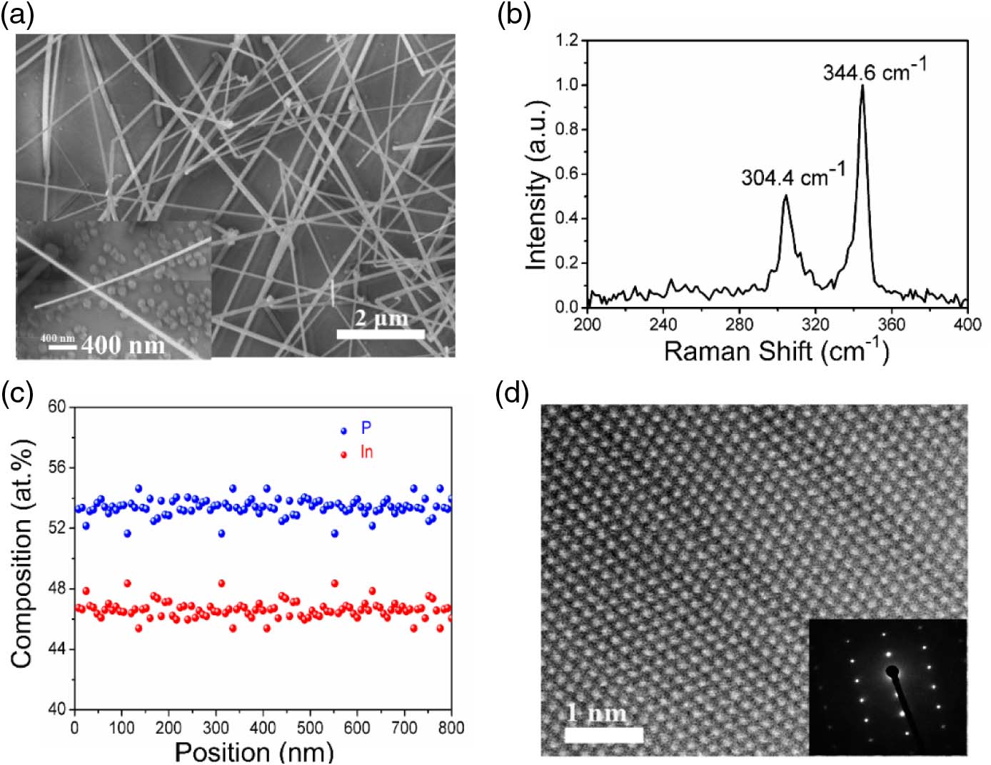
    Fig. 1. (a) SEM image of as-prepared InP NWs sample on the quartz substrate. The inset is a higher-resolution SEM image, which shows the diameter of our NWs at 65  nm. (b) Raman spectrum of as-grown InP NWs excited by a 473 nm laser. (c) EDX measurement results of InP NWs along the growth direction which show the uniformity of the as-grown NWs. (d) High-resolution STEM image of InP NWs. The inset shows the selected area electron diffraction (SAED) pattern, which demonstrates the ZB crystal structure of our InP NWs sample.
    (a) Experimental setup of the open-aperture Z-scan measurement. (b) Open-aperture Z-scan measurement results. (c) Nonlinear transmittance of the prepared InP NWs.
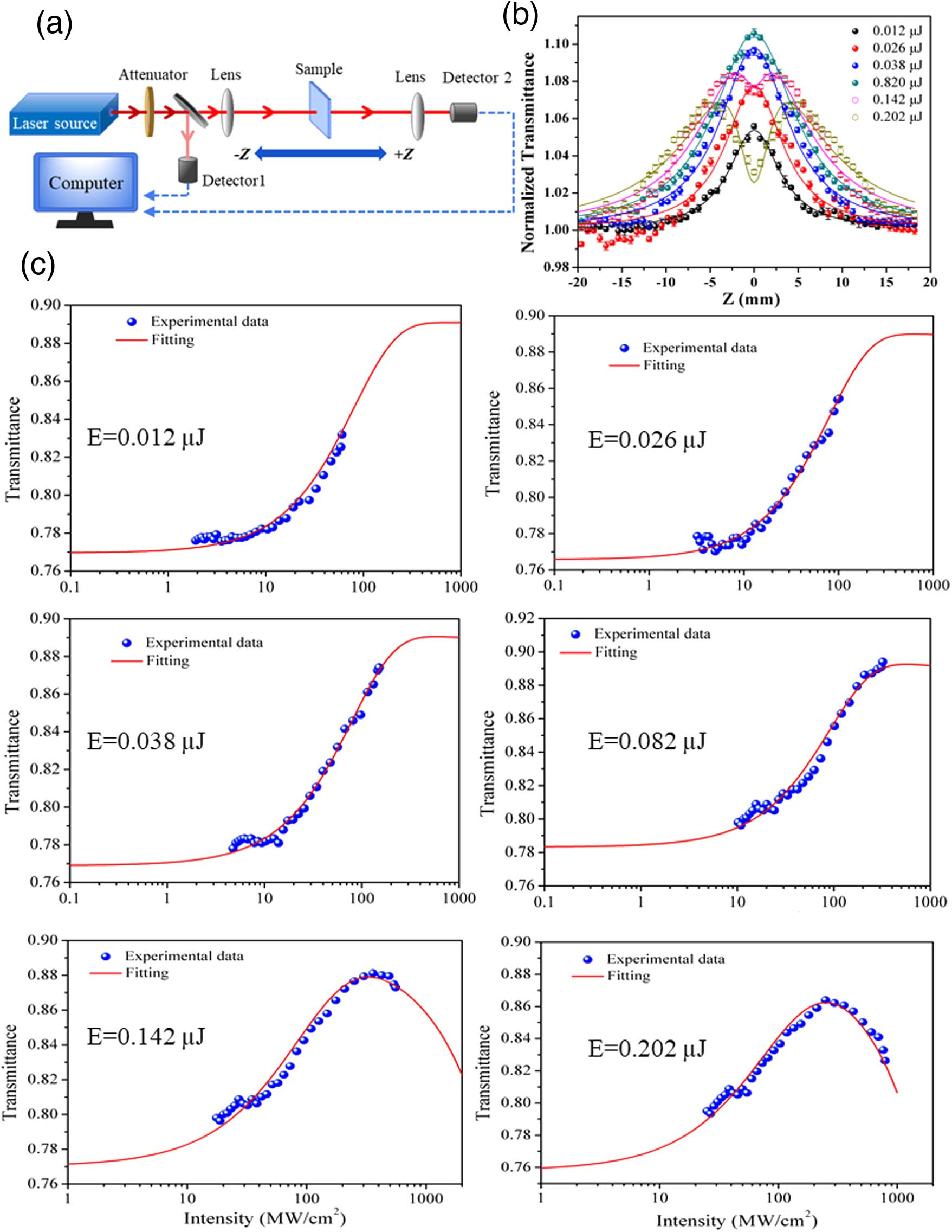
    Fig. 2. (a) Experimental setup of the open-aperture Z-scan measurement. (b) Open-aperture Z-scan measurement results. (c) Nonlinear transmittance of the prepared InP NWs.
    (a) Experimental setup of the InP NWs based PQS Nd:YVO4 solid-state laser. (b) The relationship between the continuous-wave (CW) and PQS laser output power and the absorbed pump power. (c) The variation of the pulse repetition rate and the pulse width as functions of the absorbed pump power. (d) The typical PQS pulse profiles and pulse trains.
    Fig. 3. (a) Experimental setup of the InP NWs based PQS Nd:YVO4 solid-state laser. (b) The relationship between the continuous-wave (CW) and PQS laser output power and the absorbed pump power. (c) The variation of the pulse repetition rate and the pulse width as functions of the absorbed pump power. (d) The typical PQS pulse profiles and pulse trains.
    (a) Experimental setup of the ultrafast pump–probe measurement. (b) Ultrafast transient of InP NWs with a probe laser at 800 nm.
    Fig. 4. (a) Experimental setup of the ultrafast pump–probe measurement. (b) Ultrafast transient of InP NWs with a probe laser at 800 nm.
    Input Pulse Energy (μJ)βeff (cm/MW)Imχ(3) (×107  esu)Is (MW/cm2)ΔRαNSβeff (cm/MW)
    0.012304±1.33.43±0.01580.9±0.40.121±0.0010.109±0.0030.016±0.001
    0.026272±2.13.07±0.02480.2±0.30.12±0.0020.1±0.0020.077±0.002
    0.038236±1.62.66±0.01880.3±0.50.122±0.0010.109±0.0010.13±0.01
    0.082116.5±1.41.3±0.02790.38±0.40.11±0.0030.106±0.0020.27±0.03
    0.14290.6±0.70.123±0.0020.106±0.0024.2±0.1
    0.20285.87±0.30.132±0.0010.109±0.0019.9±0.3
    Table 1. Summary of βeff, Imχ(3), βeff, and Saturable Absorption Properties of InP NWs at Different Pulse Energies
    Junting Liu, Hongkun Nie, Bingzheng Yan, Kejian Yang, He Yang, Vladislav Khayrudinov, Harri Lipsanen, Baitao Zhang, Jingliang He. Nonlinear optical absorption properties of InP nanowires and applications as a saturable absorber[J]. Photonics Research, 2020, 8(6): 1035
    Download Citation