Abstract
Indium phosphide (InP) nanowires (NWs) have attracted significant attention due to their exotic properties that are different from the bulk counterparts, and have been widely used for light generation, amplification, detection, modulation, and switching, etc. Here, high-quality InP NWs were directly grown on a quartz substrate by the Au-nanoparticle assisted vapor-liquid-solid method. We thoroughly studied their nonlinear optical absorption properties at 1.06 μm by the open-aperture Z-scan method. Interestingly, a transition phenomenon from saturable absorption (SA) to reverse saturable absorption (RSA) was observed with the increase of the incident laser intensity. In the analysis, we found that the effective nonlinear absorption coefficient () under the SA process was 3 orders of magnitude larger than that during the RSA processes. Furthermore, the SA properties of InP NWs were experimentally verified by using them as a saturable absorber for a passively -switched solid-state laser at 1.06 μm, where the shortest pulse width of 462 ns and largest single pulse energy of 1.32 μJ were obtained. Moreover, the ultrafast carrier relaxation dynamics were basically studied, and the intra-band and inter-band ultrafast carrier relaxation times of 8.1 and 63.8 ps, respectively, were measured by a degenerate pump–probe method with the probe laser of 800 nm. These results well demonstrate the nonlinear optical absorption properties, which show the excellent light manipulating capabilities of InP NWs and pave a way for their applications in ultrafast nanophotonic devices.1. INTRODUCTION
Indium phosphide (InP), an attractive direct bandgap III-V semiconductor, has been extensively studied since the early 1980s and widely used for light generation, amplification, detection, modulation, and switching [1–6]. In the past two decades, nanostructured [zero-dimensional, one-dimensional (1D), two-dimensional (2D)] III-V semiconductors have attracted growing interest because of their unique electrical, mechanical, chemical, and optical properties [7–12]. Like their 2D counterpart, quasi-1D nanowires (NWs) are regarded as promising nanoscale building blocks of the active and integrated nanosystems [7,13–15]. As a member of the 1D III-V NW family, the optical and electronic properties of InP NWs are distinct from their bulk counterpart, leading to the possibility of higher density integration [16–18]. In addition, the electrical and optical properties of NWs can be modulated by controlling their composition, shape, size, and surroundings [19–23]. Moreover, the growth of InP NWs has a large lattice mismatch tolerance, which offers many more flexibilities in the substrate selection and mechanical properties. These advantages make InP NWs a promising candidate for integrated electronic and photonic devices, as well as for the development of various kinds of heterostructures [24–26]. To date, myriads of InP NW-based devices have been successfully demonstrated, such as light-emitting diodes, photodetectors, field-effect transistors, and solar cells [24,25]. Compared with the electronic properties, studies on the nonlinear optical properties of InP NWs have been relatively rarely reported.
InP NWs have proved to exhibit strong room-temperature photoluminescence and broad emission band due to the low surface recombination velocity and free carrier recombination dynamics across mixed-phase Type II homojunction [27,28]. In addition, because of the Lorentz local field effect, InP NWs have a larger nonlinear susceptibility compared with their bulk form and show strong nonlinear absorption effect [29]. In particular, they show nonlinear saturable absorption (SA) properties originating from the Pauli blocking effect, in which two identical electrons cannot fill the same state, resulting in the bleaching of light absorption (most of the incident light is not absorbed, resulting in high transmission). The SA property makes InP NWs a promising candidate for the saturable absorber, which is widely used for pulsed laser generation. The broadband absorption of InP NW arrays, the crystal-structure-dependent photoluminescence from InP NWs, and the nonlinear optical processes of trapped InP NWs have been recently reported [20,23,29–31]. However, there are rare reports about the nonlinear absorption properties based on InP NWs.
In this paper, we first fabricated high-quality InP NWs by directly growing them on a quartz substrate using the Au nanoparticle-assisted vapor-liquid-solid (VLS) method. Then, the nonlinear optical absorption properties of NWs were thoroughly studied by the open-aperture Z-scan method with a picosecond laser source operating at 1.06 μm. A transition phenomenon from SA to reverse saturable absorption (RSA) with the increase of the laser pulse energy was observed. In the SA process, a large effective nonlinear absorption coefficient () was obtained with other negligible lossy RSA processes, which is 3 orders lower during the RSA process. Furthermore, the prepared InP NWs were used as a saturable absorber for a passively -switched solid-state laser operating at 1.06 μm, generating the shortest pulse width of 462 ns and single pulse energy of 1.32 μJ, respectively. In addition, ultrafast carrier relaxation times were checked by the pump–probe technique, which showed their great potential for the applications in the ultrafast optics devices. Our experimental results clearly demonstrate the nonlinear optical absorption properties of InP NWs, which provide a platform for the designing of III-V semiconductor NW-based photonic devices for the light manipulations.
Sign up for Photonics Research TOC. Get the latest issue of Photonics Research delivered right to you!Sign up now
2. RESULTS AND DISCUSSION
A. InP NWs Preparation and Characterization
In this work, InP NWs were grown on the quartz substrates inside a horizontal flow atmospheric pressure metalorganic vapor phase epitaxy system. Trimethylindium (TMIn) and tertiarybutylphosphine (TBP) were used as the precursors of InP NWs. The substrates were first immersed in acetone and isopropanol inside an ultrasonic bath, and then rinsed in de-ionized water for 2 min. 40 nm diameter gold (Au) nanoparticles (NPs) from a colloidal solution (BBI International, UK) were used as catalysts for VLS growth of InP. First, poly-L-lysine solution was dropped onto the substrate and kept 1 min in air to enhance the NPs adhesion. Then, Au NPs were deposited onto the substrate and kept 1 min in the air before drying the substrate with a nitrogen gun. Prior to growth, the substrates were annealed in situ at 650°C for 10 min under hydrogen flow to desorb the surface contaminants. The growth of InP NWs was performed by introducing the TMIn and TBP sources simultaneously inside the reactor while keeping the temperature at 430°C for 5 min. During the growth, the TMIn and TBP flows were 80 and 100 sccm (standard cubic centimeters per minute), respectively, resulting in the nominal V/III ratio of . After the growth, the TMIn source was switched off while keeping the TBP flow on until the reactor cooled down to 200°C to protect the NW surface from decomposition.
The surface morphologies of the as-grown InP NWs were examined by scanning electron microscopy (SEM). The SEM image in Fig. 1(a) shows that the as-grown InP NWs have an average length of –10 μm (ranging from 2 to 18 μm) and an average diameter of (ranging from 30 to 110 nm) with smooth surfaces [seen from the high-resolution SEM image inset in Fig. 1(a), and the corresponding distributions in Fig. 1(a)]. Figure 1(b) shows the Raman spectrum of the InP NWs excited by a 473 nm laser. Two typical Raman peaks located at 304.4 and are corresponding to a transverse optical and a longitudinal optical phonon mode [32], respectively, which verifies the good quality of our sample. The energy-dispersive X-ray spectroscopy (EDX) along the growth direction was measured and shown in Fig. 1(c), which illustrates the purity of our InP NW sample solely consisting of In and P without additional elements. The high-resolution scanning transmission electron microscopy (HRSTEM) was performed to determine the crystal structure of the prepared InP NWs. The typical HRSTEM image shown in Fig. 1(d) verifies the predominantly zinc blende (ZB) structure with the twin defects.
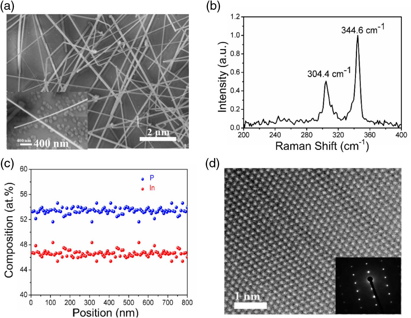
Figure 1.(a) SEM image of as-prepared InP NWs sample on the quartz substrate. The inset is a higher-resolution SEM image, which shows the diameter of our NWs at . (b) Raman spectrum of as-grown InP NWs excited by a 473 nm laser. (c) EDX measurement results of InP NWs along the growth direction which show the uniformity of the as-grown NWs. (d) High-resolution STEM image of InP NWs. The inset shows the selected area electron diffraction (SAED) pattern, which demonstrates the ZB crystal structure of our InP NWs sample.
B. Nonlinear Optical Absorption Properties
Nonlinear optical absorption properties play a significant role in the nonlinear processes including ultrafast optical switch and modulation, self-focusing, optical sensing, solitons, and so on. In this work, the nonlinear optical absorption properties of InP NWs were studied in detail by a set of home-made open-aperture Z-scan measurements, as shown in Fig. 2(a). A picosecond pulsed laser operating at 1064 nm with a pulse width of 13 ps and a repetition rate of 500 kHz was used as the excitation laser. A lens with a focal length of 60 mm was used to focus the excited picosecond laser with a Rayleigh length of 3.8 mm. Balanced detectors were selected to eliminate the unnecessary errors caused by the power jitter. The incident photon energy is about 1.16 eV, which is below the intrinsic electronic bandgap of the ZB structure InP NW () [33]. However, we experimentally observed the nonlinear optical absorption properties, which might be mainly attributed to the surface and phosphorus vacancy defects [Fig. 1(c), EDX results], which caused electrically active states in the forbidden gap [2,3,34], as well as the trapping source via two-photon (TPA) and multi-photon (MPA) absorption processes [29]. This phenomenon deserves further more detailed studies.

Figure 2.(a) Experimental setup of the open-aperture Z-scan measurement. (b) Open-aperture Z-scan measurement results. (c) Nonlinear transmittance of the prepared InP NWs.
The transmittance curves as a function of the incident laser intensity from the open-aperture Z-scan measurements can clearly reveal the nonlinear absorption information of the sample. There are many kinds of nonlinear absorption phenomena, which can be simply divided into SA and RSA (e.g., TPA, MPA, and free-carrier absorption). It should be noticed that there must be a significant Rayleigh scattering during the Z-scan measurement. However, what we concern is the transmission variation under different incident laser intensities at 1064 nm. Thus, it can be considered as the linear optical loss and has no effect on the nonlinear optical absorption response in our experiment. The Z-scan curves under different incident laser energies (intensities) are shown in Fig. 2(b). The largest laser pulse energy of our laser source was limited to . First, we found the typical SA features: where the transmittance increases as the sample is moving to the beam waist (), i.e., the incident light intensity increases, forming a transmission peak at the waist. Interestingly, when the incident laser energy was increased to 0.142 μJ, a depletion curve appeared, which illustrated the phenomenon of RSA. To understand the nonlinear absorption properties of InP NWs, we first analyze the absorption coefficient, which is written as [35] where and are the linear and nonlinear absorption coefficients, respectively; is the incident laser intensity. Based on the nonlinear optical theory, the light attenuation during propagating through an optical material can be expressed as where is the propagating distance in the material. With Eqs. (1) and (2), can be obtained by fitting the Z-scan curves, listed in Table 1. In detail, can be calculated with the following formula [36,37]: where is the vacuum light speed, and is the linear refractive index. Table 1 summarizes the values of and at the incident pulse energies of 0.012, 0.026, 0.038, and 0.082 μJ. The maximum value of and is and , which is larger than those of graphene oxide, molybdenum disulphide (), and black phosphorus. Moreover, (and ) is not a constant but shows a decreasing trend as the incident pulse energy increases. These results indicate that SA and RSA coexist, and SA dominates the nonlinear absorption process at low incident pulse intensities. However, as the incident laser intensity increases, RSA becomes more and more significant, as illustrated in Fig. 2(b). It seems RSA dominates the nonlinear absorption process under higher laser intensity excitation. These results verify the strong nonlinear optical response and optical signal modulating capabilities of InP NWs.
| Input Pulse Energy (μJ) | βeff (cm/MW) | Im χ(3) (×10−7 esu) | Is (MW/cm2) | ΔR | αNS | βeff′ (cm/MW) |
| 0.012 | −304±1.3 | −3.43±0.015 | 80.9±0.4 | 0.121±0.001 | 0.109±0.003 | 0.016±0.001 |
| 0.026 | −272±2.1 | −3.07±0.024 | 80.2±0.3 | 0.12±0.002 | 0.1±0.002 | 0.077±0.002 |
| 0.038 | −236±1.6 | −2.66±0.018 | 80.3±0.5 | 0.122±0.001 | 0.109±0.001 | 0.13±0.01 |
| 0.082 | −116.5±1.4 | −1.3±0.027 | 90.38±0.4 | 0.11±0.003 | 0.106±0.002 | 0.27±0.03 |
| 0.142 | — | — | 90.6±0.7 | 0.123±0.002 | 0.106±0.002 | 4.2±0.1 |
| 0.202 | — | — | 85.87±0.3 | 0.132±0.001 | 0.109±0.001 | 9.9±0.3 |
Table 1. Summary of , , , and Saturable Absorption Properties of InP NWs at Different Pulse Energies
Based on the two-level system, we can well explain the saturable absorption properties of low-dimensional semiconductors originating from the Pauli blocking effect. Here, considering the contribution of RSA to the nonlinear absorption effect, the absorption coefficient can be re-written as where is the remaining effective absorption coefficient, and is the saturation intensity. Combined with Eq. (2), the nonlinear optical transmittance can be expressed as [38] where is the thickness of the sample, is nonsaturation loss, and is the modulation depth. Figure 2(c) shows the nonlinear optical transmittance as a function of the incident laser intensity under the incident pulse energies of 0.012, 0.026, 0.038, 0.082, 0.142, and 0.202 μJ, respectively. By fitting the nonlinear optical transmittance as a function of the incident laser intensity with Eq. (5), , , , and can be obtained and the results are shown in Table 1. Note that RSA contribution to the nonlinear absorption () is positive and shows an increasing trend with the pulse energy increase, indicating that the RSA dominates the nonlinear absorption at higher incident laser intensity. From Fig. 2(c), it can be seen that the transition laser intensity is . When the incident laser intensity is lower than , the value of is 3 orders of magnitude smaller than that of , implying that the contribution of RSA to nonlinear absorption can be negligible. However, when the laser intensity is larger than , the transmittance decreases and a valley-like Z-scan curve appears [shown in Fig. 2(b)]. Further increasing the laser intensity to tens of , it exhibits a clear RSA behavior for open Z-scan measurement, which is consistent with previous reports of bulk InP [38]. From the obtained saturation intensity, the modulation depth, and the nonsaturable loss, it shows great potential for InP NWs to work as a saturable absorber for the generation of pulsed (e.g., passively -switched, mode-locked) lasers.
C. Nonlinear Optical Absorption Properties
In this study, we examine the InP NWs performance working as a saturable absorber in the solid-state laser system. The experimental setup is shown in Fig. 3(a). An a-cut crystal with the dimensions of was used as the gain medium. The pump source was a fiber-coupled laser diode operating at 808 nm with the fiber core diameter and numerical aperture of 400 μm and 0.22 μm, respectively. The pump laser was focused onto the crystal with a beam spot radius of 200 μm by a optical coupling system. The was wrapped with indium foil and mounted in a copper heat sink cooled with water at the temperature of 18°C. The input coupler with a curvature radius of 100 mm was anti-reflectivity coated at 808 nm and high reflectivity coated at 1064 nm. The output coupler was a flat mirror with a transmission of 10% at 1064 nm. The laser output power was measured by a laser power meter and the laser pulse characteristics were detected by a PIN photodetector and recorded by an oscilloscope.
Figure 3.(a) Experimental setup of the InP NWs based PQS solid-state laser. (b) The relationship between the continuous-wave (CW) and PQS laser output power and the absorbed pump power. (c) The variation of the pulse repetition rate and the pulse width as functions of the absorbed pump power. (d) The typical PQS pulse profiles and pulse trains.
The laser first operated in the continuous-wave (CW) regime without the InP NWs. After inserting the InP NWs into the laser cavity, the stable passively Q-switched (PQS) laser output can be realized by carefully adjusting the resonator. Figure 3(b) shows the relationship between the output power and the absorbed pump power. The maximum average output power, under PQS state, of 241 mW was obtained, giving the corresponding slope efficiency of 13.4% and CW to PQS conversion efficiency of 22.7%. The pulse width and repetition rate as functions of the absorbed pump power are shown in Fig. 3(c). The shortest pulse width of 462 ns was obtained with the corresponding pulse repetition rate of 183 kHz. The typical shortest pulse profile is shown at the top of Fig. 3(d), while the pulse train with the largest pulse repletion rate of 183 kHz is shown at the bottom of Fig. 3(d). The pulse-to-pulse instability was determined to be less than 4.83%, and the output power instability was measured to be for 2 h operation. The single pulse energy and pulse peak power are calculated to be 1.32 μJ and 2.85 W with the output power, the pulse repetition rate, and the pulse width. The output laser beam quality factor was measured to be and for the horizontal and perpendicular directions by the knife-edge method. The PQS output performances are comparable to that of InAs NWs and other 2D layered materials [39,40], indicating that InP NWs are a good candidate saturable absorber for pulsed laser generation and other photonic devices.
D. Ultrafast Carrier Relaxation Times of InP NWs
Carrier dynamics (ultrafast carrier relaxation times) of a semiconductor is important for its optoelectronic and photonic applications. In this study, the ultrafast carrier relaxation time of the as-prepared InP NWs was measured by a degenerate ultrafast pump–probe method. The experimental setup is schematically shown in Fig. 4(a). A femtosecond Ti:sapphire laser operating at 800 nm with a pulse width of 100 fs and the repetition rate of 1.0 kHz was employed. The output ultrafast laser was split into two parts: one was used as the pump laser to excite the sample, while the other was used as the probe laser to detect the pump-induced transmission variation of the sample. The pump and probe lasers were focused onto the same sample position with the pump beam spot of about 10 times larger than that of the probe laser. A Si detector with a lock-in amplifier was used to detect the optical signals.
Figure 4.(a) Experimental setup of the ultrafast pump–probe measurement. (b) Ultrafast transient of InP NWs with a probe laser at 800 nm.
Figure 4(b) shows the measured time-dependent normalized probe laser transmission () changes of the prepared InP NWs at room temperature, where is the probe laser transmittance before excitation, and is the corresponding probe laser transmission change after excitation. The positive signal shown in Fig. 4(b) reveals the photobleaching characteristic caused by the Pauli blocking effect, indicating the saturable absorption response of the prepared InP NWs. A pure quartz substrate was measured under the same condition, in which no transient response was detected, confirming that the dynamic response was solely attributed to the InP NWs. The relaxation process can be generally fitted by a bi-exponential decay model: where and are the relative amplitudes of the double temporal components, and and are the typical intra- and inter-band relaxation times. By using Eq. (6), and are determined to be 8.1 and 63.8 ps, respectively, which indicates that InP NWs have great potential for ultrafast optical signal processing.
3. CONCLUSIONS
In conclusion, high-quality InP NWs were fabricated by using an Au nanoparticle-assisted VLS growth method. The intra-band and inter-band ultrafast carrier relaxation times were measured to be 8.1 and 63.8 ps, respectively, by a degenerate pump–probe method at 800 nm. The nonlinear optical absorption properties at 1.06 μm were studied by an open-aperture Z-scan measurement, indicating a saturable absorption feature with a nonlinear absorption coefficient and an imaginary part of the third-order susceptibility of and , respectively. The absorption at 1.06 μm is mainly attributed to the surface and phosphorus vacancy defects that caused electrically active states in the forbidden bandgap. Moreover, the prepared InP NWs were used in a PQS solid-state laser operating at 1064 nm, generating the shortest pulse width of 462 ns and single pulse energy of 1.32 μJ. This work indicates that InP NWs are good saturable absorber candidates that can provide a new platform for designing III-V semiconductor NWs related photonic and optoelectronic devices.
Acknowledgment
Acknowledgment. V. K. acknowledges the support of Aalto University Doctoral School. We acknowledge the provision of facilities and technical support by Aalto University at Micronova Nanofabrication Centre.
References
[1] H. Temkin, B. V. Dutt, W. A. Bonner. Photoluminescence study of native defects in InP. Appl. Phys. Lett., 38, 431-433(1981).
[2] J. D. Dow, R. E. Allen. Surface defects and Fermi-level pinning in InP. J. Vac. Sci. Technol., 20, 659-661(1982).
[3] M. Alatalo, R. M. Nieminen, M. J. Puska, A. P. Seitsonen, R. Virkkunen. Phosphorus vacancy in InP: a negative-U center. Phys. Rev. B, 47, 6381-6384(1993).
[4] A. Marceaux, S. Loualiche, O. Dehaese, B. Lambert. High-speed 1.55 μm Fe-doped multiple-quantum-well saturable absorber on InP. Appl. Phys. Lett., 78, 4065-4067(2001).
[5] Z. Wang, B. Tian, M. Pantouvaki, W. Guo, P. Absil, J. Van Campenhout, C. Merckling, D. Van Thourhout. Room-temperature InP distributed feedback laser array directly grown on silicon. Nat. Photonics, 9, 837-842(2015).
[6] S. Yu, X. B. Fan, X. Wang, J. Li, Q. Zhang, A. Xia, S. Wei, L. Z. Wu, Y. Zhou, G. R. Patzke. Efficient photocatalytic hydrogen evolution with ligand engineered all-inorganic InP and InP/ZnS colloidal quantum dots. Nat. Commun., 9, 4009(2018).
[7] H. Pettersson, J. Trägårdh, A. I. Persson, L. Landin, D. Hessman, L. Samuelson. Infrared photodetectors in heterostructure nanowires. Nano Lett., 6, 229-232(2006).
[8] H. Yang, V. Khayrudinov, V. Dhaka, H. Jiang, A. Autere, H. Lipsanen, Z. Sun, H. Jussila. Nanowire network–based multifunctional all-optical logic gates. Sci. Adv., 4, eaar7954(2018).
[9] X. Liu, Q. Guo, J. Qiu. Emerging low-dimensional materials for nonlinear optics and ultrafast photonics. Adv. Mater., 29, 1605886(2017).
[10] A. A. Balandin, D. L. Nika. Phononics in low-dimensional materials. Mater. Today, 15, 266-275(2012).
[11] A. Cresti, N. Nemec, B. Biel, G. Niebler, F. Triozon, G. Cuniberti, S. Roche. Charge transport in disordered graphene-based low dimensional materials. Nano Res., 1, 361-394(2008).
[12] Q. Tang, Z. Zhou. Graphene-analogous low-dimensional materials. Prog. Mater. Sci., 58, 1244-1315(2013).
[13] S. A. Dayeh, D. P. Aplin, X. Zhou, P. K. Yu, E. T. Yu, D. Wang. High electron mobility InAs nanowire field-effect transistors. Small, 3, 326-332(2007).
[14] Y. Huang, X. Duan, C. M. Lieber. Nanowires for integrated multicolor nanophotonics. Small, 1, 142-147(2005).
[15] R. R. LaPierre, A. C. E. Chia, S. J. Gibson, C. M. Haapamaki, J. Boulanger, R. Yee, P. Kuyanov, J. Zhang, N. Tajik, N. Jewell, K. M. A. Rahman. III-V nanowire photovoltaics: review of design for high efficiency. Phys. Status. Solidi RRL, 7, 815-830(2013).
[16] B. Lassen, M. Willatzen, R. Melnik, L. C. L. Y. Voon. Electronic structure of free-standing InP and InAs nanowires. J. Mater. Res., 21, 2927-2935(2011).
[17] Y. Kitauchi, Y. Kobayashi, K. Tomioka, S. Hara, K. Hiruma, T. Fukui, J. Motohisa. Structural transition in indium phosphide nanowires. Nano Lett., 10, 1699-1703(2010).
[18] R. R. LaPierre, M. Robson, K. M. Azizur-Rahman, P. Kuyanov. A review of III-V nanowire infrared photodetectors and sensors. J. Phys. D, 50, 123001(2017).
[19] Y. Liang, L. Zhai, X. Zhao, D. Xu. Band-gap engineering of semiconductor nanowires through composition modulation. J. Phys. Chem. B, 109, 7120-7123(2005).
[20] N. Anttu, A. Abrand, D. Asoli, M. Heurlin, I. Åberg, L. Samuelson, M. Borgström. Absorption of light in InP nanowire arrays. Nano Res., 7, 816-823(2014).
[21] H. Yu, J. Li, R. A. Loomis, L. W. Wang, W. E. Buhro. Two- versus three-dimensional quantum confinement in indium phosphide wires and dots. Nat. Mater., 2, 517-520(2003).
[22] M. Li, J. C. Li. Size effects on the band-gap of semiconductor compounds. Mater. Lett., 60, 2526-2529(2006).
[23] M. Mattila, T. Hakkarainen, M. Mulot, H. Lipsanen. Crystal-structure-dependent photoluminescence from InP nanowires. Nanotechnology, 17, 1580-1583(2006).
[24] C. Jia, Z. Lin, Y. Huang, X. Duan. Nanowire electronics: from nanoscale to macroscale. Chem. Rev., 119, 9074-9135(2019).
[25] L. N. Quan, J. Kang, C. Z. Ning, P. Yang. Nanowires for photonics. Chem. Rev., 119, 9153-9169(2019).
[26] J. Deng, Y. Su, D. Liu, P. Yang, B. Liu, C. Liu. Nanowire photoelectrochemistry. Chem. Rev., 119, 9221-9259(2019).
[27] K. Pemasiri, M. Montazeri, R. Gass, L. M. Smith, H. E. Jackson, J. Yarrison-Rice, S. Paiman, Q. Gao, H. H. Tan, C. Jagadish, X. Zhang, J. Zou. Carrier dynamics and quantum confinement in type II ZB-WZ InP nanowire homostructures. Nano Lett., 9, 648-654(2009).
[28] G. L. Tuin, M. T. Borgström, J. Trägårdh, M. Ek, L. R. Wallenberg, L. Samuelson, M. E. Pistol. Valence band splitting in wurtzite InP nanowires observed by photoluminescence and photoluminescence excitation spectroscopy. Nano Res., 4, 159-163(2010).
[29] F. Wang, P. J. Reece, S. Paiman, Q. Gao, H. H. Tan, C. Jagadish. Nonlinear optical processes in optically trapped InP nanowires. Nano Lett., 11, 4149-4153(2011).
[30] N. Huang, C. Lin, M. L. Povinelli. Broadband absorption of semiconductor nanowire arrays for photovoltaic applications. J. Opt., 14, 024004(2012).
[31] S. J. Gibson, B. van Kasteren, B. Tekcan, Y. Cui, D. van Dam, J. E. M. Haverkort, E. Bakkers, M. E. Reimer. Tapered InP nanowire arrays for efficient broadband high-speed single-photon detection. Nat. Nanotechnol., 14, 473-479(2019).
[32] A. J. Lohn, T. Onishi, N. P. Kobayashi. Optical properties of indium phosphide nanowire ensembles at various temperatures. Nanotechnology, 21, 355702(2010).
[33] M. P. Persson, H. Q. Xu. Electronic structure of [100]-oriented free-standing InAs and InP nanowires with square and rectangular cross sections. Phys. Rev. B, 73, 125346(2006).
[34] M. Levinson, J. L. Benton, H. Temkin, L. C. Kimerling. Defect states in electron bombarded n-InP. Appl. Phys. Lett., 40, 990-992(1982).
[35] Q. Bao, H. Zhang, Y. Wang, Z. Ni, Y. Yan, Z. X. Shen, K. P. Loh, D. Y. Tang. Atomic-layer graphene as a saturable absorber for ultrafast pulsed lasers. Adv. Funct. Mater., 19, 3077-3083(2009).
[36] Y. Song, Y. Chen, X. Jiang, W. Liang, K. Wang, Z. Liang, Y. Ge, F. Zhang, L. Wu, J. Zheng. Nonlinear few-layer antimonene-based all-optical signal processing: ultrafast optical switching and high-speed wavelength conversion. Adv. Opt. Mater., 6, 1701287(2018).
[37] X. Jiang, S. Liu, W. Liang, S. Luo, Z. He, Y. Ge, H. Wang, R. Cao, F. Zhang, Q. Wen. Broadband nonlinear photonics in few-layer MXene Ti3C2Tx (T = F, O, or OH). Laser Photonics Rev., 12, 1700229(2018).
[38] F. Zhang, G. Liu, Z. Wang, T. Tang, X. Wang, C. Wang, S. Fu, F. Xing, K. Han, X. Xu. Broadband nonlinear absorption properties of two-dimensional hexagonal tellurene nanosheets. Nanoscale, 11, 17058-17064(2019).
[39] B. Guo. 2D noncarbon materials-based nonlinear optical devices for ultrafast photonics [Invited]. Chin. Opt. Lett., 16, 020004(2018).
[40] J. Liu, V. Khayrudinov, H. Yang, Y. Sun, B. Matveev, M. Remennyi, K. Yang, T. Haggren, H. Lipsanen, F. Wang, B. Zhang, J. He. InAs-nanowire-based broadband ultrafast optical switch. J. Phys. Chem. Lett., 10, 4429-4436(2019).


