• Journal of Semiconductors
  • Vol. 40, Issue 5, 052101 (2019)
P Mallika Bramaramba Devi, G. Phaneendra Reddy, and K. T. Ramakrishna Reddy
Author Affiliations
  • Solar Energy Laboratory, Department of Physics, Sri Venkateswara University, Tirupati-517502, India
  • show less
    DOI: 10.1088/1674-4926/40/5/052101 Cite this Article
    P Mallika Bramaramba Devi, G. Phaneendra Reddy, K. T. Ramakrishna Reddy. Structural and optical studies on PVA capped SnS films grown by chemical bath deposition for solar cell application[J]. Journal of Semiconductors, 2019, 40(5): 052101 Copy Citation Text show less
    (Color online) Schematic diagram of preparation of PVA capped SnS films.
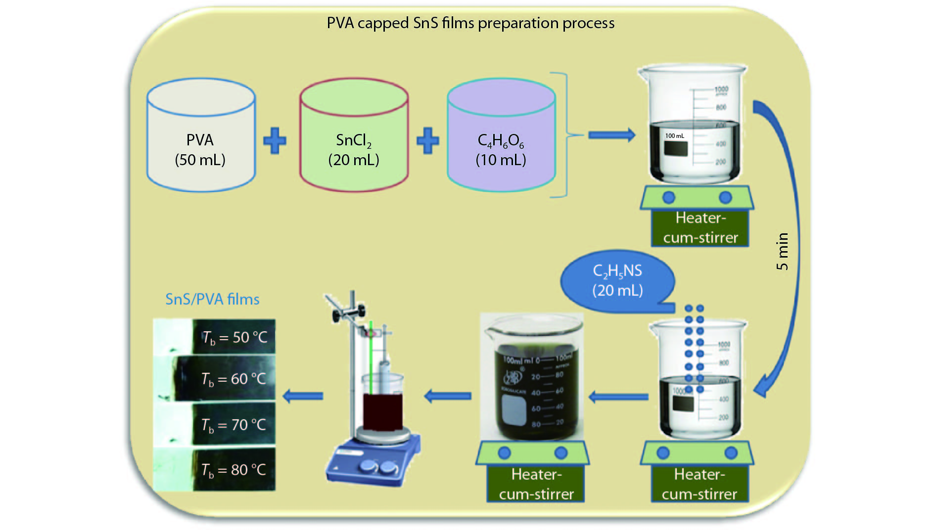
    Fig. 1. (Color online) Schematic diagram of preparation of PVA capped SnS films.
    (Color online) X-ray diffraction patterns of SnS films grown at different bath temperatures.
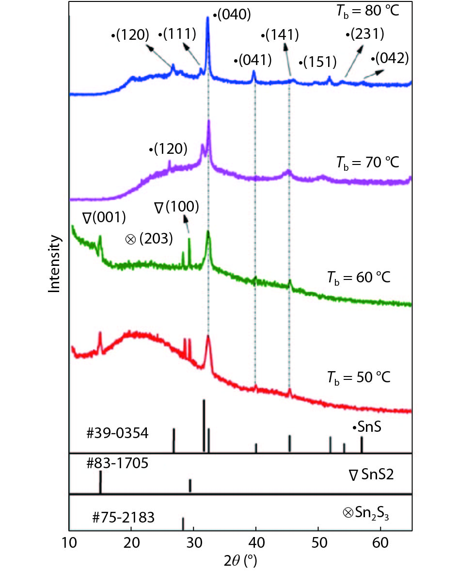
    Fig. 2. (Color online) X-ray diffraction patterns of SnS films grown at different bath temperatures.
    (Color online) Change of crystallite size and dislocation density with bath temperature.
    Fig. 3. (Color online) Change of crystallite size and dislocation density with bath temperature.
    (Color online) Variation of strain and number of crystallites per unit area of SnS layers with bath temperature.
    Fig. 4. (Color online) Variation of strain and number of crystallites per unit area of SnS layers with bath temperature.
    (Color online) W-H plots of SnS layers with bath temperature.
    Fig. 5. (Color online) W-H plots of SnS layers with bath temperature.
    (Color online) Rietveld refinement of SnS layers capped by PVA at 80 °C bath temperature.
    Fig. 6. (Color online) Rietveld refinement of SnS layers capped by PVA at 80 °C bath temperature.
    (Color online) Deconvoluted Raman spectra of SnS layers grown at different bath temperatures.
    Fig. 7. (Color online) Deconvoluted Raman spectra of SnS layers grown at different bath temperatures.
    (Color online) FTIR pectra of SnS layers grown at different bath temperatures.
    Fig. 8. (Color online) FTIR pectra of SnS layers grown at different bath temperatures.
    (Color online) SEM images of SnS layers grown at different bath temperatures (a) 50 °C, (b) 60 °C , (c) 70 °C, and (d) 80 °C.
    Fig. 9. (Color online) SEM images of SnS layers grown at different bath temperatures (a) 50 °C, (b) 60 °C , (c) 70 °C, and (d) 80 °C.
    (Color online) 2D and 3D AFM micrographs of SnS layers formed at different bath temperatures (a) 60 °C, (b) 70 °C, and (c) 80 °C.
    Fig. 10. (Color online) 2D and 3D AFM micrographs of SnS layers formed at different bath temperatures (a) 60 °C, (b) 70 °C, and (c) 80 °C.
    (Color online) Variation of optical transmittance as a function wavelength in SnS films.
    Fig. 11. (Color online) Variation of optical transmittance as a function wavelength in SnS films.
    (Color online) Change of absorption coefficient as a function of photon energy in the SnS films. (Inset) Tauc plots of SnS films.
    Fig. 12. (Color online) Change of absorption coefficient as a function of photon energy in the SnS films. (Inset) Tauc plots of SnS films.
    Deposition methodDeposition temperature (°C)PhaseSn/S ratioα (cm–1) Band gap (eV)Ref.
    CBD (uncapped)40–80SnS1041.41–1.30[47]
    Sulfurization150–450SnS (300–350 °C), SnS + Sn2S3 (150– 200 °C), SnS + SnS2 (400–450 °C) 1.2–1.6[48]
    Thermal evaporation200–400SnS0.96-1.101.36[49]
    RF sputtering150–300SnS1.67–1.44[50]
    MOCVD430–470SnS0.92–1.321041.3–1.1[51]
    Spray pyrolysis250–450SnS (250–400 °C), SnS + Sn2S3 (450 °C) 1.29–1.111.70–1.46[52]
    Electron beam evaporation300SnS1.38[11]
    CVD200–400SnS2.77–1.15[53]
    Spin coating150–400SnS (200 °C), SnS + SnS2 (300 °C), SnS + Sn2S3 (400 °C) 1.31–1.031.88–1.26[54]
    CBD (PVA capping)50–80SnS (70–80 °C), SnS + Sn2S3 + SnS2 (70– 80 °C) 0.46–0.951051.92–1.55Present work
    Table 1. Data of the SnS thin films deposited on glass substrates at different deposition temperatures reported in literature.
    Tb (°C) FWHM (°)dXRD (Å) dJCPDS (Å) D (nm) δ (1015 lines/m2) ε (10–3) N (1015)
    Scherrer’s formulaW-H plotScherrer’s formulaW-H plot
    500.760482.8282.835114.07.811.822.462.4
    600.724342.8272.835124.37.011.122.253.8
    700.407192.8252.83521102.26.17.89.7
    800.386932.8232.83522112.05.96.98.4
    Table 2. Structural parameters of PVA capped SnS layers formed at different bath temperatures with respect to (040) plane.
    Bath temperature (°C)Sn (at.%)S (at.%)Sn/S
    5030.2465.500.46
    6036.3660.660.59
    7046.1551.530.89
    8048.2650.280.95
    Table 3. Atomic weight (at.%) composition determined using EDS at different bath temperatures.
    Tb (°C) Particle size from XRD analysis (nm)Particle size from AFM micrographs analysis (nm)Particle size from optical measure-ments (nm)
    504.05.1
    604.34.95.3
    70105.36.1
    80117.68.4
    Table 4. Comparison of particle size of SnS nanocrystals capped by PVA estimated using XRD, AFM and optical measurements.
    P Mallika Bramaramba Devi, G. Phaneendra Reddy, K. T. Ramakrishna Reddy. Structural and optical studies on PVA capped SnS films grown by chemical bath deposition for solar cell application[J]. Journal of Semiconductors, 2019, 40(5): 052101
    Download Citation