
P Mallika Bramaramba Devi, G. Phaneendra Reddy, K. T. Ramakrishna Reddy. Structural and optical studies on PVA capped SnS films grown by chemical bath deposition for solar cell application[J]. Journal of Semiconductors, 2019, 40(5): 052101
- Journal of Semiconductors
- Vol. 40, Issue 5, 052101 (2019)
Abstract
1. Introduction
Recent investigations on photovoltaic devices emphasize the importance of semiconducting metal chalcogenide thin film solar cells at low cost. The IV–VI group semiconductors are highly attractive for their novel properties suitable for optoelectronic applications and can be synthesized by using simple techniques in thin film form. Tin monosulphide (SnS) belongs to this group of materials that has three stable binary phases, SnS, SnS2 (both layer structures) and Sn2S3 (ribbon structure)[
It is known that due to high surface to volume ratio and quantum size effects, the nanostructured materials offer great advantages than the bulk materials. Various reports are available on synthesis of SnS nanoparticles using different techniques[
Few works on synthesis of various semiconducting nanostructures capped by PVA are reported[
2. Experimental details
2.1. Chemicals
In the present study, stannous chloride (SnCl2, 2H2O) was used as the source material for tin and thioacetamide (C2H5NS) for sulphur. Tartaric acid (C4H6O6) was used as a complexing agent and polyvinyl alcohol (–CH2CHOH–)n (average M.W. = 1 60 000) as capping agent to prepare SnS thin films.
2.2. Method
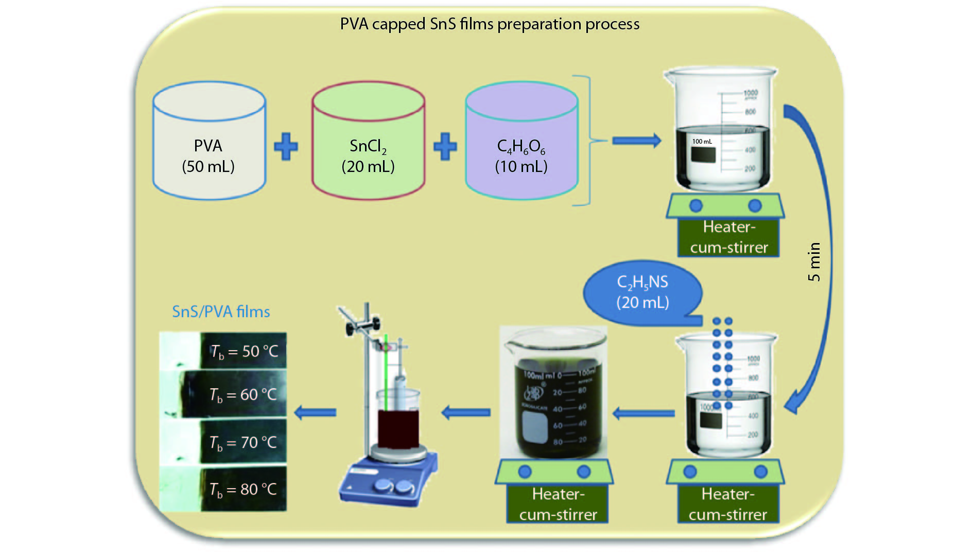
The PVA capped SnS thin films were prepared using chemical bath deposition as shown in Fig. 1. Initially, 2 g of PVA was dissolved in 100 mL water, contained in a beaker and stirred at 80 °C by using a magnetic stirrer, which has a facility to control the temperature until a viscous transparent solution was obtained and then allowed to cool to the room temperature. Fresh solutions of 0.1 M stannous chloride (SnCl2, 2H2O), 0.2 M thioacetamide (C2H5NS) and 0.5 M tartaric acid were prepared using double distilled water such that the precursor ratio of S/Sn was maintained as 2. Initially, 20 mL of stannous chloride and 10 mL of tartaric acid were added to 50 mL of previously prepared PVA solution in a glass beaker and stirred well by a magnetic stirrer at a rate of 200 revolutions per minute. After 5 min, 20 mL of thioacetamide was added to the solution Lsuch that the total volume of the solution becomes 100 mL. Now, cleaned glass substrates were immersed vertically into the solution to deposit SnS films. The deposition of SnS films were carried out for a fixed time of 90 min at different bath temperatures that varied from 50 to 80 °C. The deposited films were cleaned using distilled water and dried in a hot air oven. The visual observation of the deposited layers indicated dark brown colour and the films were well adherent to the glass substrate surface without any visible pinholes and cracks.
![]()
Figure 1.(Color online) Schematic diagram of preparation of PVA capped SnS films.
The deposited SnS layers were characterized using appropriate techniques. The X-ray diffraction patterns of the layers deposited on glass substrates at different bath temperatures were recorded using Burker (D8 Advance) X-ray diffractometer, using CuKα (λ = 1.5408 Å) radiation at room temperature. The Raman spectra were recorded in the backscattering configuration at room temperature with unpolarized light using DIPOLAR XY 800 Raman spectrometer. FTIR absorption spectra for the deposited experimental films were recorded using Thermo Nicolet FTIR spectrophotometer. The morphology of the layers was observed by using a Carl Zeiss EVO 50 scanning electron microscope (SEM). Solver Nano NT-MDT atomic force microscope (AFM) was used to investigate the surface roughness of the films. The optical transmittance measurements were carried out using JASCO V-770 UV-VIS-NIR spectrophotometer, using unpolarized light.
3. Results and discussions
3.1. Structural analysis
3.1.1. X-ray diffraction studies
X-ray diffraction analysis was undertaken to investigate the structural properties of the deposited SnS layers. Fig. 2 shows the typical X-ray diffraction patterns of SnS films capped by PVA at different temperatures that varied in the range of 50–80 °C. The XRD spectrum indicated many peaks in all the deposited films with an intense (040) peak observed at 2θ = 32.0°. In addition, all the observed peaks were broad, indicating nanocrystalline nature of the grown layers. The films deposited at bath temperatures < 70 °C exhibited secondary phases such as Sn 2S3 and SnS2 in addition to SnS. The peaks observed at 2θ = 15.02° and 2θ = 28.39° corresponds to (001) and (100) planes of SnS2 and the peak at 2θ = 27.73° corresponds to (203) plane of Sn2S3 respectively that matches with the standard data reported in JCPDS card no. 83-1705 and 75-2183. Also the peaks observed at 2θ = 26.02°, 31.50°, 39.40° and 44.88°, 51.42° 53.89° 56.73° corresponds to (120), (111), (041), (141), (151), (231) and (042) planes of SnS phase with orthorhombic crystal structure as reported in JCPDS card no. 39-0354. Kalandragh et al.[
![]()
Figure 2.(Color online) X-ray diffraction patterns of SnS films grown at different bath temperatures.
Various structural parameters such as the average crystallite size, dislocation density, strain and number of crystallites per unit area were evaluated using X-ray diffraction data. The interplanar spacing dhkl was calculated using the Bragg’s diffraction principle,
where n is an integer, λ is the wavelength of X-rays (1.5408 Å) and θ is the Bragg’s diffraction angle.
The average crystallite size (D) of the layers was calculated using Debye-Scherrer formula[
where K is the shape factor, which is equal to 0.94 and
The calculated crystallite size varied with bath temperature in the range, 11–22 nm, indicating an increasing trend with bath temperature. From this, it can be understood that with the increase of bath temperature, there will be an increase in kinetic energy of the reactants, which in turn increases the formation of nuclei on the surface of the substrate.
The dislocation density (δ) was determined using the following relation[
Fig. 3 shows the change of crystallite size and dislocation density with bath temperature. It can be seen from the Fig. that values of δ varied in the range, 7.8 × 10¹⁵–2.0 × 10¹⁵ m–2 with the increase of bath temperature from 50 to 80 °C. A minimum value of δ was observed for the layers grown at 80 °C due to improved crystallinity. This is because of the fact that the dislocations present at lower bath temperatures received more thermal energy at higher bath temperatures and hence moved from inside the crystallites to their grain boundaries and neutralized.
![]()
Figure 3.(Color online) Change of crystallite size and dislocation density with bath temperature.
The lattice strain (
where the symbols have usual meaning.
The evaluated strain values (shown in Fig. 4) decreased from 1.18 × 10⁻² to 5.9 × 10⁻³ with the increase of bath temperature. This indicates that the strain in the layers deposited at lower bath temperature was higher due to the presence of crystal imperfections and dangling bonds. At higher temperatures there was a decrease in the lattice strain due to an increase in crystallite size and a decrease in dislocation density as the higher growth temperatures could annihilate the defects. The number of crystallites per unit area (N) was calculated using the relation[
![]()
Figure 4.(Color online) Variation of strain and number of crystallites per unit area of SnS layers with bath temperature.
where t is the thickness of the films, ~ 90 nm as determined from SEM cross-section. Fig. 4 also shows the variation of number of crystallites with the increase of bath temperature. The number of crystallites per unit area varied between 6.2 × 10¹⁶ and 8.4 × 10¹⁵ with the raise of bath temperature from 50 to 80 °C. This is because of the fact that higher temperatures could provide higher thermal energy so that small crystallites coalesce together to form big ones, leading to the formation of large crystallites.
In XRD peaks, the observed broadening is considered to be due to the sum of contributions by the crystallite size and strain distribution present within the sample. Thus the crystallite size estimated from Scherrer’s equations could be different from the actual crystallite size. Therefore, those contributions of size and strain must be separated by a more elaborated analysis, such as Williamson-Hall (W-H) plot. The average crystallite size and residual strain were described using the following equation[
Fig. 5 shows the W-H plots of the deposited SnS layers at bath temperatures varied from 50 to 80 °C. The intercept of the linear fit on the y-axis gives the average crystallite size and the slope of the linear fit gives the corresponding residual strain value. The estimated average crystallite size varied in the range, 4–11 nm and the strain values varied in the range, 2.24 × 10⁻² to 6.9 × 10⁻³ nm with bath temperature were given in the Table 2. Thus the average crystallite size increases and the strain decreases with increase in bath temperature as was already discussed earlier. The calculated structural parameters of SnS films prepared via chemical bath deposition technique at different bath temperatures are listed in Table 2.
![]()
Figure 5.(Color online) W-H plots of SnS layers with bath temperature.
Table Infomation Is Not EnableFurther, Rietveld refinement analysis confirms the existence of orthorhombic SnS phase present in the deposited films. Fig. 6 shows the Rietveld refinement of deposited single phase SnS layers grown at 80 °C bath temperature fitted using Expo-2014 software. The good quality of fitting is represented by GOF (goodness of fit) of the Rietveld refinement, which is 1.482, indicating well resolved individual peaks. The refinement analysis shows orthorhombic crystal structure to the SnS layers, shown in the inset of Fig. 5. The lattice parameters calculated using refinement software were a = 4.091 Å, b = 11.102 Å, c = 3.970 Å. The estimated values of expected Rp factor and the weighted profile (RWP) factor are 5.780 and 7.635. Therefore, the crystalline structure of SnS did not alter by the surface modification.
![]()
Figure 6.(Color online) Rietveld refinement of SnS layers capped by PVA at 80 °C bath temperature.
3.1.2. Raman analysis
The Raman analysis was carried out for further phase confirmation on the deposited layers as it is more sensitive to structural and compositional changes in the material. Fig. 4 shows the deconvoluted Raman spectra of the synthesized films deposited at different bath temperatures that varied in the range, 50–80 °C. At lower bath temperatures (< 70 °C ), the spectra showed five characteristic peaks of tin monosulphide that appeared at 94, 166, 178, 219 and 225 cm–1. In addition to these, other peaks related to Sn2S3 phase (307 cm–1) and SnS2 phase (312 cm–1) were also observed. Films deposited at higher bath temperatures (≥ 70 °C) showed the Raman modes corresponding to tin monosulphide phase at 94, 166, 178 and 225 cm–1. In general, SnS with orthorhombic crystal structure had 21 optical phonon modes. Among these modes, 12 are Raman active (4Ag, 2Bg, 4B2g and 2B3g), 7 are infrared active (3B1u, 3B3u and 1B2u), and 2 are inactive (2Au)[
In all the deposited layers, Raman mode appeared at 94 cm–1 had the highest intensity compared to other modes. A similar trend of Raman spectra with 94 cm–1 as an intense peak was observed by Sall et al.[
![]()
Figure 7.(Color online) Deconvoluted Raman spectra of SnS layers grown at different bath temperatures.
3.2. FTIR analysis
The Fourier transform infrared spectral measurements were made for further confirmation of the interaction between PVA and SnS nanocrystals by identifying the absorbed functional groups on the crystallite surface of the grown layers. Fig. 8 shows the FTIR transmission mode spectra of the deposited PVA capped SnS layers deposited at different bath temperatures that varied in the range, 50–80 °C. The spectra showed characteristic bands of O–H, CH2, C–H, C=C and C–O groups. The characteristic band at 3757 cm–1 is due to O–H stretching vibration of hydroxyl groups of PVA. The band at 2938 cm–1 corresponds to CH2 asymmetric stretching vibration. The band at 1707 cm–1 is attributed to C = C stretching vibration. The band at 1518 cm-1 is generally ascribed to C–H bending vibration and the band at 1030 cm–1 assigned to C–O stretching of acetyl groups present in PVA. From these characteristic bands, it is confirmed the presence of PVA used in the synthesis of experimental SnS layers. In addition to these bands, the spectra showed a strong band at 2355 cm–1, which represents the characteristic band of SnS[
![]()
Figure 8.(Color online) FTIR pectra of SnS layers grown at different bath temperatures.
3.3. Surface morphology and topography
3.3.1. Morphological studies
Fig. 9 shows the SEM micrographs of SnS thin films capped by PVA grown at different bath temperatures varying from 50 to 80 °C. The morphology of SnS layers deposited at higher bath temperatures is different from those synthesized at lower bath temperatures. Layers formed at a bath temperature of 50 °C had a sponge-like structure of SnS nanocrystals and the layers deposited at 60 °C had an uneven distribution of grains due to the presence of voids. Large size and closely packed spherical shaped crystals were noticed in the films formed at 70 and 80 °C bath temperatures. This is because of an improvement in the crystallinity of the layers formed at higher temperatures due to secondary nucleation. In fact at higher temperatures, the bonds between -OH group and the nanocrystals became weak and hence an interaction occurs between more number of particles, which leads to an increase in the size of the particles[
![]()
Figure 9.(Color online) SEM images of SnS layers grown at different bath temperatures (a) 50 °C, (b) 60 °C , (c) 70 °C, and (d) 80 °C.
3.3.2. Topographical analysis
AFM analysis was carried out to study the surface topography of PVA capped SnS layers. Fig. 10 shows the 2-dimensional AFM images along with 3D images of the prepared SnS films. AFM studies shows the gradual change in surface roughness and morphology of the experimental films with varied bath temperature. The average surface roughness of SnS films capped by PVA was evaluated using the AFM data that varied in the range, 2.6–3.2 nm, where the films formed at lower temperatures had slightly higher roughness and vice versa. It is also observed from the topographical analysis that the particles grew in irregular shape with a smaller size at lower bath temperatures (< 70 °C). This is mainly due to insufficient thermal energy for the atoms and hence they could not move over the surface to form larger crystallites. However, at higher bath temperatures ( ≥ 70 °C), there is an improvement in the particle size due to secondary nucleation and the layers exhibited spherically shaped grains. This behaviour was already observed in the XRD, Raman and SEM studies. The observed average particle size obtained by AFM analysis increased from 4.9 to 7.6 nm with bath temperature.
![]()
Figure 10.(Color online) 2D and 3D AFM micrographs of SnS layers formed at different bath temperatures (a) 60 °C, (b) 70 °C, and (c) 80 °C.
3.4. Compositional analysis
The elemental compositions of the PVA capped SnS thin films as a function of bath temperature was studied using EDS technique. Table 3 shows the compositions of Sn and S elements present in the films prepared at various bath temperatures. The analysis showed the presence of Sn and S elements in the deposited films. With the increase of bath temperature from 50 to 80 °C, the Sn/S ratio of SnS films grown in this work varied in the range, 0.46–0.95. At lower bath temperatures (Tb ≤ 60 °C), the films showed sulfur rich composition, which indicates a less reaction of sulfur with Sn source in the reaction bath. As the bath temperature was increased to 70 °C and above, the composition ratio of Sn and S was increased from 0.89 to 0.95. This is because of an enhancement of reaction rate at higher bath temperatures. Films prepared at Tb = 80 °C showed the film composition close to stoichiometry (Sn/S ratio of approximately 1.0), which indicates the successful reaction in the bath.
3.5. Optical studies
The optical transmittance spectra of PVA capped SnS layers grown at different bath temperatures as a function of wavelength recorded in the range, 300–2500 nm is shown in Fig. 11. The spectra showed a decrease in optical transmittance with the increase of bath temperature, which indicates high absorbance in the layers formed at higher bath temperatures. Therefore, the absorption edge was shifted towards the red region with the increase of bath temperature. The optical absorption coefficient (α) in the absorption region was determined using the formula[
![]()
Figure 11.(Color online) Variation of optical transmittance as a function wavelength in SnS films.
where T is the transmittance and t is the thickness of the film.
The evaluated value of absorption coefficient for all layers was ~ 105 cm–1, indicating that the films were highly absorbing and therefore they may be useful as an absorber layer for photovoltaic device fabrication. A plot of absorption coefficient (α) versus hυ for deposited films formed at different bath temperatures is shown in Fig. 12. It is evident from the plot that the absorption coefficient directly varies with temperature and hence the layers formed at 80 °C has maximum absorption coefficient. The energy band gap of the films is calculated using the expression[
![]()
Figure 12.(Color online) Change of absorption coefficient as a function of photon energy in the SnS films. (Inset) Tauc plots of SnS films.
where A is constant and hυ is photon energy. The Tauc plots of (αhυ)2 versus hυ for the layers deposited at different bath temperatures are shown in the inset of Fig. 12. By extrapolating the linear portion of the curve onto the energy axis, the energy band gap was determined and an enhancement in the energy band gap has been observed for all the grown layers. The calculated energy band gap values for layers deposited decreased from 1.92 to 1.55 eV with the increase of bath temperature, which are higher than that of bulk value of SnS (1.3 eV). The observed blue shift in energy band gap values for the films deposited at bath temperatures (< 70 °C) is due to the presence of secondary phases that had higher energy band gaps. Whereas for the films deposited at bath temperatures (≥ 70 °C), the observed increase in band gap is attributed to the quantum confinement effect. A similar behaviour is also noted in the literature by Janaet al.[
Using energy band gap values, the average particle size at a particular growth temperature can be estimated using Brus equation[
where En is the energy band gap of deposited SnS films, Eg is the energy band gap of bulk SnS, me* is the effective mass of excited electron, mh* is the effective mass of excited hole, h is the Plank’s constant, e is the charge of an electron,
4. Conclusions
Tin monosulphide thin films have been successfully grown using PVA as the capping agent for the first time by chemical bath deposition technique. The layers were formed on glass substrates at different bath temperatures that varied in the range, 50–80 °C. XRD studies revealed that all the deposited films had (040) peak as the preferred orientation that corresponds to SnS. Layers formed at lower bath temperatures, < 70 °C showed secondary phases of Sn 2S3 and SnS2, which disappeared when the temperature was increased to 70 °C. The Raman spectra supported this behaviour and showed relevant modes of different phases observed at different temperatures. XRD and Raman studies indicated an increase in crystallite size with increase of bath temperature. FTIR spectra clearly proved that the deposited SnS layers were capped by PVA. SEM analysis exhibited an increase of grain size with bath temperature whereas AFM studies indicated a decrease in surface roughness and an increase in particle size with the increase of bath temperature. The optical studies showed a direct optical absorption in the films. Optical band gap enhancement has been observed, where the energy band gap decreased from 1.92 to 1.55 eV with the increase of bath temperature. The single phase nanocrystalline PVA capped SnS layers may find application in the development of photovoltaic devices.
References
[1] A T Kana, T G Hibbert, M F Mahon et al. Organotin unsymmetric dithiocarbamates: Synthesis, formation and characterization of tin (II) sulphide films by atmospheric pressure chemical vapour deposition. Polyhedron, 20, 2989(2001).
[2] K T R Reddy, N K Reddy, R W Miles et al. Photovoltaic properties of SnS based solar cells. Sol Energy Mater Sol Cells, 90, 3041(2006).
[3] E Guneri, F Gode, C Ultas et al. Effect of deposition time on structural, electrical, optical properties of SnS thin films deposited by chemical bath deposition. App Surf Sci, 257, 1189(2010).
[4] N K Reddy, K T R Reddy. Optical behaviour of sprayed tin sulphide thin films. Mater Res Bull, 41, 414(2006).
[5] Y Kawano, J Chantana, T Minemoto et al. Impact of growth temperature on the properties of SnS films prepared by thermal evaporation and its photovoltaic performance. Curr Appl Phys, 15, 897(2015).
[6] M Ganchev, P Vitanvov, M Sendova-Vassileva et al. Properties of SnS thin films grown by physical vapour deposition. J Phys: Conf Ser, 682, 012019(2016).
[7] S Cheng, Y Chen, Y He et al. The structure and properties of SnS thin films prepared by pulse electro deposition. Mater Lett, 61, 1408(2007).
[8] M M EI-Nahass, H M Zeyada, M S Aziz et al. Optical properties of thermally evaporated SnS thin films. Opt Mater, 20, 159(2002).
[9] J A Andrade-Arvizu, M F Garcia-Sanchez, M Courel-Piedrahita et al. Suited growth parameters including type of conductivity conversions on chemical spray pyrolysis synthesized SnS thin films. J Anal Appl Pyrolysis, 121, 347(2016).
[10] K O Haraa, S Suzuki, N Usami et al. Formation of metastable cubic phase in SnS thin films fabricated by thermal evaporation. Thin Solid Films, 639, 7(2017).
[11] A Tanusevski, D Poelman. Optical and photoconductive properties of SnS thin films prepared by electron beam evaporation. Sol Energy Mater Sol Cells, 80, 297(2003).
[12] V Ana, M Dronova, A Zakharov et al. Optical and AFM studies on p-SnS films deposited by magnetron sputtering. Chalcogenide Lett, 12, 483(2015).
[13] S Banu, S J Ahn, Y J Eo et al. Thin monosulphide (SnS) thin films grown by liquid-phase deposition. Solar Energy, 145, 33(2017).
[14] S Jana, R Thapa, R Maity et al. Optical and dielectric properties of PVA capped nanocrystalline PbS thin films synthesized by chemical bath depostition. Physica E, 40, 3121(2008).
[15] E P Subramaniam, G Rajesh, N Muthukumarasamy et al. Solar cells of Cu2ZnSnS4 thin films prepared by chemical bath deposition method. Indian J Pure Ap Phy, 52, 620(2014).
[16] J Jing, M Cao, C Wu et al. Chemical bath deposition of SnS nanosheet thin films for FTO/SnS/CdS/Pt photocathode. J Alloys Compd, 726, 720(2017).
[17] U Chalapathi, B Poornaprakash, S H Park et al. Chemically deposited cubic SnS thin films for solar cell applications. Solar Energy, 139, 238(2016).
[18] S H Chaki, M D Chaudhary, M P Deshpande. SnS thin films deposited by chemical bath deposition, dip coating and SILAR. J Semicond, 37, 053001(2016).
[19] M T S Nair, P K Nair. Simplified chemical bath deposition for good quality SnS thin films. Semicond Sci Technol, 6, 132(1991).
[20] P K Nair, M T S Nair, V M Garcia et al. Semiconductor thin films by chemical bath deposition for solar energy related applications. Sol Energy Mater Sol Cells, 52, 313(1998).
[21] M Reighima, A Akkari, C Guasch, N T Kamoun et al. Synthesis and characterization of Fe-doped SnS thin films by chemical bath deposition technique for solar cell applications. J Renew Sustain Energy, 5, 063109(2013).
[22] K S Kumar, C Manoharan, S Dhanapandian et al. Effect of Sb dopant on the structural, optical and electrical properties of SnS thin films by spray pyrolysis technique. Spectrochimica Acta A, 115, 840(2013).
[23] S H Chaki, M D Chaudhary, M P Deshpande et al. Effect of indium and antimony doping in SnS single crystal. Mater Res Bull, 63, 173(2015).
[24] H Kafasham, R Ebrahimi-Kahrizsangi, F Jamali-Sheini et al. Effect of Al doping on the structural and optical properties of electrodeposited SnS thin films. Phys Status Solidi A, 5, 1302(2016).
[25] K G Deepa, J Nagaraju. Growth and photovoltaic performance of SnS quantum dots. Mater Sci Eng B, 177, 1023(2012).
[26] F Alam, V Dutta. Tin sulphide (SnS) nanostructured films deposited by continuous spray pyrolysis (CoSP) technique for dye-sensitized solar cell applications. Appl Surf Sci, 358, 491(2015).
[27] J Park, C H Hwang, W Young Lee et al. Preparation of size tunable SnS nanoparticles by a sonochemical method under multibubble sonoluminescence conditions. Mater Lett, 117, 188(2014).
[28] Y Azizian-Kalandaragh, A Khodayari, Z Zeng et al. Strong quantum confinement effects in SnS nanocrystals produced by ultrasound-assisted method. J Nanoparticle Res, 15, 1388(2013).
[29] P Babu, M V Reddy, G Sreedevi et al. Status review on earth-abundant and environmentally green Sn–X (X = Se, S) nanoparticle synthesis by solution methods for photovoltaic applications. Int J Hydrog Energy, 42, 2790(2017).
[30] V Bala, M Sharma, S K Tripathi et al. Investigations of AI: CdS/PVA nanocomposites: A joint theoretical and experimental approach. Mater Chem Phys, 146, 523(2014).
[31] M Ramrakhiani, V Nogriya. Photo and electro-luminescence of cadmium selenide nanocrystals and nanocomposites. J Lumin, 133, 129(2013).
[32] J J L Hmar, T Majumder, S P Mondal et al. Growth and characteristics of PbS/polyvinyl alcohol nanocomposites for flexible high dielectric thin film applications. Thin Solid Films, 598, 243(2016).
[33] I S Elashmawi, A M Abdelghany, N A Hakeema et al. Quantum confinement effects of CdS nanoparticles dispersed within PVP/PVA nanocomposites. J Mater Sci Mater Electron, 24, 2956(2014).
[34] S K M Begum, G Nirmala, K Ravindranadh et al. Physical and spectral investigations of Mn2+ ions doped poly vinyl alcohol capped ZnSe nanoparticles. J Mol Struct, 1006, 344(2011).
[35] A Zakaria, R Zamiri, P Vaziri et al. Thermal diffusivity measurement of cadmium sulphide nanoparticles prepared by
[36] P Sagitha, K Sarada, K Muralidharan et al. One pot synthesis of poly vinyl alcohol (PVA) supported silver nanoparticles and its efficiency in catalytic reduction of methylene blue. Trans Nonferrous Met Soc China, 26, 2693(2016).
[37] G Murugadoss, M Rajesh kumar. Synthesis and optical properties of monodispersed Ni2+ doped ZnS nanopaarticles. Appl Nanosci, 4, 67(2014).
[38] J Osuntokun, P A Ajibade. Morphology and thermal studies of zinc sulphide and cadmium sulphide nanoparticles in polyvinyl alcohol matrix. Physica B, 496, 106(2016).
[39] S A Mohamed, A A AI-Ghamdi, G D Sharma et al. Effect of ethylene carbonate as a plasticizer on CuI/PVA nanocomposite: Structure, optical and electrical properties. J Adv Res, 5, 79(2014).
[40] R Seoudi, S A EI Mongy, A A Shabaka et al. Effect of polyvinyl alocohol matrices on the structural and spectroscopic studies of CdSe nanoparticles. Physica B, 403, 1781(2008).
[41] M Sharma, S K Tripathi. Optical and electrical properties of polyvinyl alcohol doped CdS nanoparticles prepared by sol–gel method. J Mater Sci Mater Electron, 26, 2760(2015).
[42] I S Elashmawi, N A Hakeema, M Soliman Selim et al. Optimization and spectroscopic studies of CdS/polyvinyl alcohol nanocomposites. Mater Chem Phys, 115, 132(2009).
[43] Y S Tamgadge, A L Sunatkari, S S et al. Linear and nonlinear optical properties of nanostructured Zn(1–
[44] N Singh, R M Mehra, A Kapoor. ZnO based quantum dot sensitized solar cell using CdS quantum dots. J Renew Sustain Energy, 4, 013110(2012).
[45] P Phukan, D Saikia. Optical and structural investigation of CdSe quantum dots dispersed in PVA matrix and photovoltaic applications. Int J Photoenergy, 2013, 728280(2013).
[46] D Saikia, P Phukan. Fabrication and evaluation of CdS/PbS thin film solar cell by chemical bath deposition technique. Thin Solid Films, 562, 239(2014).
[47] G Sreedevi, M V Reddy, C Park et al. Comprehensive optical studies on SnS layers synthesized by chemical bath deposition. Opt Mater, 42, 468(2015).
[48] V R M Reddy, G Sreedevi, C Park et al. Development of sulphurized SnS thin film solar cells. Curr Appl Phys, 15, 588(2015).
[49] S N Nwankwo, S Campbell, K T R Reddy et al. Temperature controlled properties of sub-micron thin SnS films. Semicond Sci Technol, 33, 065002(2018).
[50] D H Hwang, J Y Shin, S Lee et al. Substrate temperature effects on the properties of radio-frequency sputtered SnS thin films. Nanosci Nanotechnol Lett, 10, 696(2018).
[51] A J Clayton, C M E Charbonneau, W C Tsoi et al. One-step growth of thin film SnS with large grains using MOCVD. Sci Technol Adv Mater, 19, 153(2018).
[52] T Sall, B M Soucase, M Mollar et al. SnS thin films prepared by chemical spray pyrolysis at different substrate temperatures for photovoltaic applications. J Electron Mater, 46, 1714(2017).
[53] K Assilli, K Alouani, X Vilanova. Impact of deposition temperature on the properties of SnS thin films grown over silicon substrate- comparative study of structural and optical properties with films grown on glass substrates. Semicond Sci Technol, 32, 115005(2017).
[54] M Al Shakban, Z Xie, N Savjani et al. A facile method for the production of SnS thin films from melt reactions. J Mater Sci, 51, 6166(2016).
[55] N S Saenk. The X-ray diffraction study of three-dimensional disordered network of nanographites: experiment and theory. Physics Procedia, 23, 102(2012).
[56] A Purohit, S Chander, S P Nehra et al. Effect of air annealing on structural, optical, morphological and electrical properties of thermally evaporated CdSe thin films. Physica E, 69, 342(2015).
[57] K Sarmah, R Sarma, H L Das. Structural characterization of thermally evaporated CdSe thin films. Chalcogenide Lett, 5, 153(2008).
[58] S A J Jassim, A A R Ali Zumaila et al. Influence of substrate temperature on the structural, optical and electrical properties of CdS thin films deposited by thermal evaporation. Results in Physics, 3, 173(2013).
[59] Y T Prabhu, K V Rao, V S S Kumar et al. X-ray analysis by Williamson-Hall and size-strain methods of ZnO nanoparticles with fuel variation. World J Nano Sci Eng, 4, 21(2014).
[60] B H Baby, V M Vaisakh, D B Mohan et al. Fabrication and phase characterization study of SnS thin films under controlled sulfur deposition temperature. Mater Today, 3, 2077(2016).
[61] S Ali, F Wang, S Zafar et al. Characterization and Raman vibrations of chalcogenide SnS nanorods. IOP Conference Series: Materials Science and Engineering, 275, 012007(2017).
[62] Y Jayasree, U Chalapathi, P U Bhaskar et al. Effect of precursor concentration and bath temperature on the growth of chemical bath deposited tin sulphide thin films. Appl Surf Sci, 258, 2732(2012).
[63] A M S Arulanantham, S Valanarasu, K Jeyadheepan et al. Development of SnS (FTO/CdS/SnS) thin films by nebulizer spray pyrolysis (NSP) for solar cell applications. J Mol Struct, 1152, 137(2018).
[64] D Das, R K Dutta. A novel method of synthesis of small band gap SnS nanorods and its efficient photocatalytic dye degradation. J Colloid Interface Sci, 457, 339(2015).
[65] D C Onwudiwe, T P J Kruger, O S Oluwatobi et al. Nanosecond laser irradiation synthesis of CdS nanoparticles in a PVA system. Appl Surf Sci, 290, 18(2014).
[66] P R Guddeti, S Gedi, K T R Reddy et al. Sulfurization temperature dependent physical properties of Cu2SnS3 films grown by a two-stage process. Mater Sci Semicond Process, 86, 164(2018).
[67] K S Ojha. Structural and optical properties of PVA doped zinc sulphide thin films. Optik, 127, 2586(2016).
[68] L Brus. Electronic wave functions in semiconductor clusters: experiment and theory. J Phys Chem, 90, 2555(1986).
[69] J Xu, Y Yang. Study on the performances of SnS heterojunctions by numerical analysis. Energy Convers Manag, 78, 260(2014).

Set citation alerts for the article
Please enter your email address
© Copyright 2018-2021 | Chinese Laser Press. All Rights Reserved 沪ICP备15018463号-20