
Liang Zhang, Yanan Guo, Jianchang Yan, Qingqing Wu, Yi Lu, Zhuohui Wu, Wen Gu, Xuecheng Wei, Junxi Wang, Jinmin Li. Deep ultraviolet light-emitting diodes based on well-ordered AlGaN nanorod array[J]. Photonics Research, 2019, 7(9): B66
- Photonics Research
- Vol. 7, Issue 9, B66 (2019)
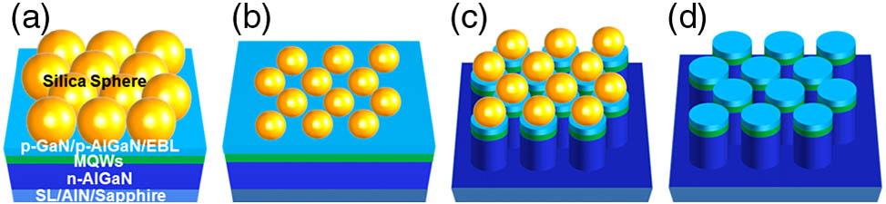
Fig. 1. Schematic diagrams of the DUV LEDs nanorod structure fabrication process. (a) SiO 2 CF 4 SiO 2
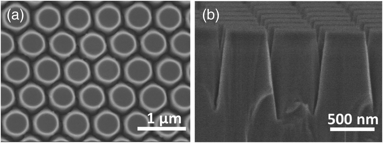
Fig. 2. (a) Top-view and (b) cross-sectional SEM images of nanorod array structure.
Fig. 3. TDPL band peak positions for (a) nanorod and (b) planar DUV LEDs and (c) their Arrhenius plots of the normalized PL intensities as a function of temperature.
Fig. 4. Dependence of the (a) integrated PL intensity, (b) PL relative efficiency, and (c) peak photon energy on excitation-energy density at room temperature for two samples.
Fig. 5. (a) TRPL spectra of the planar and nanorod DUV LEDs at room temperature. Time-dependent carrier density extracted for (a) and scaled to (b) 1 / [ I ( t ) ] 1 / 2 1 / 2 ) ln [ I ( t ) ]
Fig. 6. Fabrication process of nanorod DUV LED devices. (a) Depositing SiO 2 SiO 2
Fig. 7. (a) EL spectra of the nanorod AlGaN DUV LED at different injection current densities (from 10 A / cm 2 120 A / cm 2 20 A / cm 2
Fig. 8. Schematic diagrams of the (a) planar and (b) nanorod DUV LEDs for FDTD computation with boundary conditions.
Fig. 9. Cross-sectional near-field electric field intensity of the investigated (a), (c) planar and (b), (d) nanorod DUV LEDs for (a), (b) TE and (c), (d) TM polarizations at x – z

Set citation alerts for the article
Please enter your email address
© Copyright 2018-2021 | Chinese Laser Press. All Rights Reserved 沪ICP备15018463号-20