Abstract
The nanorod structure is an alternative scheme to develop high-efficiency deep ultraviolet light-emitting diodes (DUV LEDs). In this paper, we first report the electrically injected 274-nm AlGaN nanorod array DUV LEDs fabricated by the nanosphere lithography and dry-etching technique. Nanorod DUV LED devices with good electrical properties are successfully realized. Compared to planar DUV LEDs, nanorod DUV LEDs present times improvement in light output power and external quantum efficiency. The internal quantum efficiency of nanorod LEDs increases by 1.2 times due to the transformation of carriers from the exciton to the free electron–hole, possibly driven by the interface state effect of the nanorod sidewall surface. In addition, the nanorod array significantly facilitates photons escaping from the interior of LEDs along the vertical direction, contributing to improving light extraction efficiency. The three-dimensional finite-different time-domain simulation is performed to further analyze in detail the TE- and TM-polarized photons extraction mechanisms of the nanostructure. Our results demonstrate the nanorod structure is a good candidate for high-efficiency DUV emitters.1. INTRODUCTION
In the last decades, deep ultraviolet light-emitting diodes (DUV LEDs) have been widely explored for their potential applications in air/water purification, disinfection, bio-medical detection, and so on [1,2]. However, at present, DUV LEDs are unsatisfactory for commercialized applications due to the low light output power (LOP) and efficiency. So far, the highest external quantum efficiency (EQE) over 20% was reported by Takano et al. [3], but the mostly reported EQEs of AlGaN multiple quantum wells (MQWs) DUV LEDs with planar structure in the UV-C (200 nm to 280 nm) region are still less than 10% [4]. Generally, the low internal quantum efficiency (IQE) and low light extraction efficiency (LEE) are two crucial contributors to the poor EQE. The former issue is attributed to high dislocation density, insufficient carrier injection, and quantum confined Stark effect (QCSE) in MQWs. And the latter issue derives mainly from the serious total internal reflection (TIR) of photons at the interface between high-refraction epitaxial layers/substrate and the ambient medium [5].
Nanorods (or nanowires) are acknowledged as a promising method to overcome the low EQE issue [6,7]. These structures can suppress the internal strain and the lateral transport of carriers in MQWs to increase the IQE [8,9]. Also, the photonic and cavity effects of nanorods (or nanowires) are also exploited to LEE [10,11]. Up to date, AlGaN nanorod (or nanowire) LEDs are obtained mostly by molecular beam epitaxy [12–14]. Moreover, the AlGaN nanowires are grown on GaN/Si or metal with p-type metal contact on top, which brings about difficulties in light extraction. Recently, AlGaN/AlN core-shell MQWs based on the regrowth on AlN nanorods have been reported, which shows a promising scheme to realize high efficiency and high output power DUV LEDs [15,16]. But that structure has not yet achieved electrically injected luminescence. Top-down etching is an economical method to realize nanorod LEDs without the aforementioned concern and has already been demonstrated in efficient InGaN/GaN-based blue LEDs [17]. However, electrically injected Al-rich AlGaN-based nanorod DUV LEDs have been extremely challenging to realize, since the nanorods are separated from each other and the fillers commonly used in visible nanorod LEDs absorb DUV photons, thus making Ohmic contact difficult to be deposited on the top surface [8].
In this paper, we employed the silica nanosphere lithography (SNL) and dry-etching technique to prepare nanorod arrays and further fabricate nanorod DUV LED devices using no filler technique. The reverse leakage current is about 0.1 μA at , embodying good electric properties. Compared to planar DUV LEDs, the LOP and EQE increase by 2.5 times. The IQE of nanorod DUV LEDs is multiplied 1.2 times at room temperature, which is possibly ascribed to the efficient dissociation of excitons via the interface effect of the nanorod sidewall surface. Moreover, the LEE also significantly increases due to the modulation of photons by the nanorod array.
Sign up for Photonics Research TOC. Get the latest issue of Photonics Research delivered right to you!Sign up now
2. EXPERIMENT
The AlGaN-based DUV LED wafer was grown by our homemade low-pressure metal–organic chemical vapor deposition (LP-MOCVD) on a 2-in c-plane sapphire substrate at 50 Torr (1 Torr = 133.322 Pa). The LED structure consisted of a 1-μm AlN template, 20 pairs of (20/20 nm) superlattices, 2-μm n-, five 3-nm QWs sandwiched by 12-nm barriers, 50-nm p-AlGaN layer, and 120-nm p-GaN. Figure 1 shows the fabrication flow diagram of the nanorod array by the SNL and dry-etching technique. First, a highly ordered self-assembled monolayer of nanospheres with the diameter of 600 nm was dip-coated on the wafer and spaced by using a -based inductively coupled plasma (ICP) etch to shrink the nanospheres to around 500 nm. Following this, the wafer was etched down to n-AlGaN via a Cl-based ICP. Finally, the residual nanospheres were removed by the buffer oxide etchant. The nanorods were treated in the mixed solution () to remove ICP-induced sidewall etching damages and clear contaminants on the surface of the nanorods at the same time. After that, the sample was dipped in hydrochloric solution () to remove the oxide layer on the surface of the nanorods.
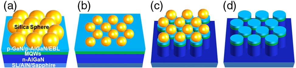
Figure 1.Schematic diagrams of the DUV LEDs nanorod structure fabrication process. (a) nanospheres deposited on the wafer. (b) -based ICP etching shrinks the nanospheres. (c) Cl-based ICP etches down wafer to n-AlGaN layer. (d) nanospheres are removed by the buffer oxide etchant.
The surface morphology of the nanorods was characterized by the field emission scanning electron microscope (SEM, Hitachi S4800). The temperature-dependent photoluminescence (TDPL), time-integrated PL (TIPL), and time-resolved PL (TRPL) were measured using a frequency-tripled fs Ti:sapphire laser with a wavelength of about 260 nm, and the optical excitation and light collection were from samples’ top surfaces. The electroluminescence (EL) spectra and the LOPs of DUV LEDs were obtained using a calibrated integrating sphere and a calibrated high-resolution spectrometer system (HAAS 2000). The angle-resolved EL spectra were measured by an angle-resolved spectrum system (R1, Ideaoptics, China) equipped with a calibrated UV-Vis-NIR PG2000-Pro spectrometer. The three-dimensional finite-difference time-domain (3D-FDTD) simulation was used to analyze the light extraction mechanisms in the nanorod array structure.
3. RESULTS AND DISCUSSION
Figures 2(a) and 2(b) show the typical top-view and cross-sectional SEM images of the nanorod array, respectively. Nanorods are in a highly uniform hexagonal array determined by ordered silica nanospheres with 600-nm pitch and a density of . The diameters of nanorods’ bottoms/tops and their heights are on average around 400 nm, 600 nm, and 1 μm, respectively. The slanted sidewalls with angles of are observed. A 300-nm-thick is deposited to coat the nanorod surface as the protective layer by the plasma-enhanced chemical vapor deposition (PECVD) as the first fabrication procedure of the nanorod DUV LED devices.

Figure 2.(a) Top-view and (b) cross-sectional SEM images of nanorod array structure.
Figures 3(a) and 3(b) show the TDPL band peak position for the nanorod and planar DUV LEDs, and their peak emission photon energies are around 4.46 eV and 4.48 eV, respectively. These two samples exhibit a so-called S-shape dependence, usually attributed to the hopping of carriers through the localized states rooted in the fluctuations of the content and interfaces of QWs [18]. Figure 3(c) shows the normalized PL intensity as a function of temperature from 10 K to 300 K in an Arrhenius plot. The IQEs were calculated to be 35% and 42% for the planar and nanorod LEDs, respectively. The IQE of the nanorod LED increased by a factor of 1.2 relative to that of the planar structure. After fabricating into the nanorod structure, the compressive strain in LEDs was alleviated, and the total polarization intensities in QWs were slightly increased as our recent work reported [19]. The increase in polarization intensity countered the increase in IQE. Also, the power-dependent PL (PDPL) suggested that the QCSE had little adverse impact on the IQE, and that will be discussed later. So, the improvement of IQE derives from other mechanisms. The nanorods would laterally confine the carriers compared to the planar structure and could enhance the electron–hole oscillator strength to contribute to the improvement of IQE [9]. In addition, Chen et al. [9] recently reported the significant improvement of the optical performance of InGaN/GaN MQW nanorods compared to their planar counterparts, because the nanorod sidewall provides an effective pathway for exciton dissociation into free electron–holes. The latter’s higher recombination rate contributes to the enhancement of optical properties. That provides us with another clue to reveal the reasons for the improved IQE for the nanorod DUV LED. Hence, we studied the excited power-dependent recombination dynamics in nanorod and planar LEDs by PL.
Figure 3.TDPL band peak positions for (a) nanorod and (b) planar DUV LEDs and (c) their Arrhenius plots of the normalized PL intensities as a function of temperature.
Figure 4(a) shows the TIPL intensity under various excited power densities. The PL intensity increases linearly with excited power density for the planar DUV LED, while that of the nanorod DUV LED exhibits an exponential increase. Here, we define this PL to be PDPL. It is clear that the PL intensity of the nanorod DUV LED is dramatically larger than that of the planar DUV LED, which roots in the higher IQE and LEE. The PL efficiency () is defined as the ratio of PL intensity to excited power density, and its dependence on excited power density at room temperature for two samples is illustrated in Fig. 4(b). The of the nanorods increases dramatically with the excited power density, whereas that of the planar LED is almost constant, suggesting different recombination mechanisms for these two samples. The increasing with the excited power density is a signature of systems dominated by the free electron–hole recombination, while the relatively flat is typical in systems dominated by exciton recombination. The PL efficiency [Eq. (1)] proposed by Chen et al. [9] is applied to describe the recombination dynamics process including the free electron–hole and exciton recombination to further confirm our speculation: where, , , and stand for the coefficients of Shockley–Read–Hall (SRH) recombination, exciton, and electron–hole recombination, respectively; is the excited power density in direct proportion to the total carrier concentration; and are coefficients.
Figure 4.Dependence of the (a) integrated PL intensity, (b) PL relative efficiency, and (c) peak photon energy on excitation-energy density at room temperature for two samples.
In an exciton dominated system, where , Eq. (1) is simplified to , which is independent of the excitation-energy density. The of the planar DUV LED is independent of the excitation-energy density, as shown in Fig. 4(b), indicating the typical exciton recombination. The of the nanorods increases with the excitation-energy density. So, the recombination rate is carrier-density dependent, which originates from the fact that free electron–hole recombination is proportional to the square of carrier concentration [20]. In fact, the exciton formation is possible only for carrier density lower than Mott density (). The carrier density studied here is lower than according to the calculation of Ref. [21], which is lower than the reported () [22]. Therefore, excitons dominate the carrier recombination in MQWs of the planar DUV LED when the injected carrier density is lower than .
Figure 4(c) shows the dependences of the peak photon energy on the excitation-energy density at room temperature for two samples. The peak photon energy of the nanorod DUV LED exhibits a red shift compared with that of the planar DUV LED, which results from the shrinking of the band gap due to strain relaxation [23,24]. Also, the interface effect caused by the nanorod sidewall surface could also contribute to the red shift [25]. The peak photon energy for both samples remains almost constant under various excitation-energy densities. The blue shift arising from the Coulomb screening effect of the QCSE does not appear [21]. The results indicate the QCSE has little adverse impact on the carrier recombination here. Because of the large band offset and narrow well width in our samples, the energy level above the triangular potential wells is high [26]. Therefore, the increased polarization intensity has a negligible impact on the IQE.
Figure 5(a) shows the TRPL spectra of the planar and nanorod DUV LEDs measured at room temperature. The TRPL spectra of these two samples both can be fitted well using exponential curves described by the following equation [9]: where () is the PL intensity as a function of time . and are two constants. The can be regarded as the radiative recombination lifetime, while the can be expressed as ( is non-radiative recombination lifetime, ) [27]. The fitted , and calculated are 15 ps, 128 ps, and 17 ps and 20 ps, 237 ps, and 21.6 ps for the nanorod and planar DUV LEDs, respectively. According to the fitting results, of the nanorod DUV LED is much smaller than that of the planar DUV LED, which clearly shows that the nanorod DUV LED exhibits a faster radiative recombination rate than the planar DUV LED, potentially indicating a higher IQE for the former. Since is much less than , the is dominated mainly by a non-radiative recombination process. Note that the temporal resolution of the detector in our TRPL measurement is , meaning that the value might be influenced by the precision of our equipment.
Figure 5.(a) TRPL spectra of the planar and nanorod DUV LEDs at room temperature. Time-dependent carrier density extracted for (a) and scaled to (b) for the bimolecular recombination model and (c) ( for the monomolecular recombination model.
Subsequently, we fitted the curve line in the TRPL by a rate equation to analyze the recombination dynamics process.
For a bimolecular recombination process [9,27], For a monomolecular recombination process [9,27], where is the injected current density, and and are constants. According to Eqs. (4) and (7), we scaled the data in Fig. 5(a), using for the bimolecular recombination [Fig. 5(b)] and for the monomolecular recombination [Fig. 5(c)]. Figure 5(b) reveals that our data of the nanorod DUV LED agree well with the bimolecular recombination mechanism corresponding to the free electron–hole recombination, while the bimolecular recombination model does not fit well the data of the planar DUV LED. In contrast, the data of the planar DUV LED agree much better with the monomolecular recombination model corresponding to the exciton recombination, but those of the nanorod DUV LED deviate from this dependence, as shown in Fig. 5(c). The results mean that the free electron–hole and the exciton dominate the recombination process in the nanorod and planar DUV LEDs, respectively. That is consistent with the results of the PDPL.
According to the analysis above, we infer there must be some driving forces to help overcome the Coulomb attraction or the binding energy of excitons to dissociate excitons into free carriers. Compared with the planar LED, the main changes in the nanorod LED are the relaxed compressive strain in the MQWs and the increased nanorod sidewall interface. The relaxed compressive strain can enhance the polarization field in the MQWs [19], which acts as a driving force to dissociate the excitons [9]. However, the peak photon energy in Fig. 4(c) does not show obvious blue shift under high excited power density, suggesting the polarization field increase might be slight. The increased nanorod sidewall interface would bring the interface state effect. On one hand, the interface states on the nanorod sidewall can result in band bending nearby and induce additional electrical field. The excitons are promoted to be dissociated into electrons and holes. Although the surface band bending would result in a spatial separation between electrons and holes and thus be harmful to radiative recombination, we think that the recombination rate reduction can be compensated by the recombination rate increase due to the transformation of recombination mechanisms. On the other hand, it is reported that some low energy states on the surface could contribute to the exciton dissociation [28]. The interface state effect of the nanorods can generate low energy levels [25]. The exciton banding energy () can be estimated by the formula , , where is the material dielectric constant, and and are the effective masses of the excited electron and hole, respectively [29]. The generated low energy levels can change the energy band structure, resulting in the decrease in or , which could reduce the to facilitate exciton dissociation.
Subsequently, the electrically injected devices were fabricated by the process shown in Fig. 6. First, the 300-nm-thick was deposited on the surface of the nanorod as the passivating and insulating layer by the PECVD, as shown in Figs. 6(a) and 6(e). It should be noted that no filler existed among the nanorods to avoid the absorption of DUV photons [30]. Then partial was removed to expose the n-AlGaN and p-GaN, as presented in Figs. 6(b) and 6(f). After that, Ti/Al/Ti/Au (20/120/20/100 nm) metal stacks were deposited on the n-AlGaN as the n-type contact using an electron beam evaporation system and annealed at 1000°C [as shown in Fig. 6(c) and the inset in Fig. 6(g)]. Ni/Au (20/20 nm) stacks were used as the p-type contact on top of the nanorods and annealed at 550°C in air [as shown in Figs. 6(c) and 6(g)]. The nanorods were separated by air voids without filler to planarize the surface of the nanorod array. Hence, a thick Al/Ti/Au (300/50/300 nm) stack metal layer was deposited on the p-contact of the nanorods to connect the p-contact together via a tilting angle deposition technique to avoid metal entering gaps among the nanorods, as depicted in Figs. 6(d) and 6(h). The inset in Fig. 6(h) clearly shows that there is little metal in the air voids among the nanorods. Afterwards, DUV LED devices were fabricated with the chip size of by the standard LED process. The devices were flip-chip bonded onto ceramic submounts, and the submounts were bonded onto metal-core printed circuit boards for better heat dissipation and device testing.
Figure 6.Fabrication process of nanorod DUV LED devices. (a) Depositing as insulating layer to passivate the surface of nanorod LEDs. (b) Partial is removed to expose n-AlGaN and p-GaN. (c) Ti/Al/Ti/Au and Ni/Au metal stacks are deposited on the n-AlGaN and p-GaN as the n-type contact and the p-type contact, respectively. (d) Al/Ti/Au stack metal layers are deposited on the p-contact of nanorods to connect p-contact together. (e)–(h) Corresponding SEM diagrams of (a), (b), (c), and (d), respectively.
Figure 7(a) depicts the room temperature EL spectra of nanorod DUV LEDs at different injection current densities (from to ). The single peak light emission is located at about 274 nm, which is approximately in line with the PL. Figure 7(b) shows the current-voltage characteristics of the planar and nanorod DUV LEDs, and their turn-on voltages are about 7 V. The inset is the current-voltage curve on a semi-log scale. It is worth noting that the reverse leakage current is about 0.1 μA for both kinds of DUV LEDs at -10 V, indicating a good fabrication process for the device. The nanorod surface treatment by mixed solution can remove the amorphous layer caused by ICP etching, which could serve as non-radiative recombination centers. Moreover, the passivates the dangling band on the surface of nanorods, preventing surface current leakage. Hence, we finally get an extremely low reverse leakage current. Figure 7(c) compares the LOP and EQE versus current for the nanorod LED with that of the planar LED. The LOP of the nanorod LED increases with injected current density, while that of the planar LED is saturated at and then decreases with injected current density. This is attributed to better heat dissipation in the nanorod LED because of the thick interconnected Al/Ti/Au metal layer on the top of the nanorods. Additionally, the planar LED suffers more obvious efficiency droop than the nanorod LED, for which the heat effect should mainly account. At , LOP and EQE of the nanorod LED approximately rise 2.5 times compared to that of the planar LED. Hence, the LEE of the nanorod LED is about 2.08 times that of the planar LED and is another more significant factor to improve EQE. We further carried out the measurement of the angular distribution EL spectra of nanorod and planar DUV LEDs at . As shown in Fig. 7(d), the emission pattern of the planar DUV LED exhibits a typical heart-like shape, which roots in the anisotropic emission pattern from photon polarization caused by the unique property of c-plane Al-rich AlGaN MQWs [31], while the radiation pattern of the nanorod DUV LED is more like the Lambertian pattern. The divergence angles (defined as the angle between the points at which the emission intensity is half the maximum [32]) of the planar LED and the nanorod LED are 120° and 140°, respectively. The latter exhibits a smaller divergence angle, indicating more photons are redirected to the vertical direction of the chip. We believe this is attributed to the vertical extraction of photons by the nanorod array structure.
Figure 7.(a) EL spectra of the nanorod AlGaN DUV LED at different injection current densities (from to ) under CW biasing condition. (b) Current-voltage characteristics of both kinds of LEDs, and the inset is the current-voltage curve on a semi-log scale. (c) LOPs and EQEs under different current densities. (d) Normalized angle-resolved EL spectra of nanorod and planar DUV LEDs measured at .
The 3D-FDTD simulation was further performed to study the light extraction mechanisms of the nanorod array. The simulated device structures of the DUV LED are depicted in Fig. 8, and the parameters of epitaxial layers were described earlier. The nanorods were surrounded by a 60-nm shell layer and oriented along the axis, which is parallel to the direction. Furthermore, an Al/Ti/Au (300/50/300 nm) stack layer was deposited on the p-contact of the nanorods as labeled in Fig. 8(b). The refractive indices for sapphire, AlN, GaN, and were set as 1.8, 2.16, 2.9, and 1.52, [31,33] respectively. The refractive indices of AlGaN were obtained by linear combinations of components of GaN and AlN [34]. The absorption coefficients of , MQWs and p-GaN were , , and 170,000 , respectively [31,33]. Perfectly matched layer (PML) boundary condition is applied to all boundaries. The computational domain was set to be in the and dimensions, respectively. A 274-nm single dipole source with 10-nm FWHM was placed at the center of the MQWs in one nanorod approximately located in the center of the device, while for the planar structure device, the single dipole was located in the center of MQWs. In addition, TE polarization is represented by the major electric field traveling in the out-of-plane direction, while TM polarization is defined as the major electric field traveling in the in-plane direction. A source power monitor placed in the bottom of the sapphire substrate was used to measure the LOP radiated out of the device, since the devices had flip-chip structure and most of the UV light would come from the backside of the sapphire.
Figure 8.Schematic diagrams of the (a) planar and (b) nanorod DUV LEDs for FDTD computation with boundary conditions.
The simulation results show that TE- and TM-polarized LEEs in the planar DUV LED are, respectively, and , which is consistent with the reported result in a previous analytical study of the planar AlGaN-based UV LED [35]. As for the nanorod DUV LED, the TE- and TM-polarized LEEs are 12% and 9%, respectively, showing, respectively, 1.6 times and 35 times higher TE-polarized and TM- polarized LEEs than the conventional planar structure. Figure 9 shows the electric field intensity distribution at the plane for the planar and nanorod DUV LEDs. We can clearly see that the TE- or TM-polarized light emitted from the MQWs of one individual nanorod can couple into the vertically directed guided modes [11], or couple into adjacent nanorods to again form vertically directed guided modes. As a consequence, the opportunity for photons escaping from the substrate side increases. The Bragg scattering caused by the highly ordered nanorod array also promotes photons extracted from the sidewall in the vertical direction. In addition, the p-GaN with downsize decreases the absorption of photons [10]. Thus, some photons transmitting to the top side can be effectively reflected back to the substrate side by the planar Al/Ti/Au stack layer and probably escape out [36]. These reasons can also explain the enhanced vertical emission in the light output angular distribution.
Figure 9.Cross-sectional near-field electric field intensity of the investigated (a), (c) planar and (b), (d) nanorod DUV LEDs for (a), (b) TE and (c), (d) TM polarizations at plane, respectively.
4. CONCLUSION
In summary, we have fabricated nanorod DUV LEDs by the SNL and dry-etching process and prepared the nanorod DUV LED devices using no filler technique. Compared to planar DUV LEDs, nanorod DUV LEDs demonstrate about times increase in LOP and EQE, which can be attributed mainly to the improvement of IQE and LEE. The dissociation of excitons into free electron–holes contributes to the increased IQE for the higher recombination rate of free carriers. In addition, the nanorod array facilitates the extraction of DUV photons via the waveguide effect, Bragg scattering effect, and reflection of the planar Al/Ti/Au stack layer on top of the nanorods. These findings reveal the carrier recombination dynamics and light extraction mechanism in nanorod DUV LEDs and will pave a good way for high-efficiency DUV emitters.
Acknowledgment
Acknowledgment. The authors thank Ideaoptics Inc. for support on the angle-resolved spectrum measurements.
References
[1] D. Li, K. Jiang, X. Sun, C. Guo. AlGaN photonics: recent advances in materials and ultraviolet devices. Adv. Opt. Photon., 10, 43-110(2018).
[2] J. M. Li, Z. Liu, Z. Q. Liu, J. C. Yan, T. B. Wei, X. Y. Yi, J. X. Wang. Advances and prospects in nitrides based light-emitting-diodes. J. Semicond., 37, 061001(2016).
[3] T. Takano, T. Mino, J. Sakai, N. Noguchi, K. Tsubaki, H. Hirayama. Deep-ultraviolet light-emitting diodes with external quantum efficiency higher than 20% at 275 nm achieved by improving light-extraction efficiency. Appl. Phys. Express, 10, 031002(2017).
[4] M. Kneissl, T.-Y. Seong, J. Han, H. Amano. The emergence and prospects of deep-ultraviolet light-emitting diode technologies. Nat. Photonics, 13, 233-244(2019).
[5] Y. Guo, J. Yan, Y. Zhang, J. Wang, J. Li. Enhancing the light extraction of AlGaN-based ultraviolet light-emitting diodes in the nanoscale. J. Nanophoton., 12, 043510(2018).
[6] R. Lin, S. V. Galan, H. Sun, Y. Hu, M. S. Alias, B. Janjua, T. K. Ng, B. S. Ooi, X. Li. Tapering-induced enhancement of light extraction efficiency of nanowire deep ultraviolet LED by theoretical simulations. Photon. Res., 6, 457-462(2018).
[7] B. S. Ooi, T. K. Ng, M. K. Shakfa, D. Priante, R. C. Subedi, I. Ashry, A. A. Alatawi, E. Stegenburgs, J. A. Holguin-Lerma, M. Tangi, M. S. Alias. Review of nanophotonics approaches using nanostructures and nanofabrication for III-nitrides ultraviolet-photonic devices. J. Nanophoton., 12, 043508(2018).
[8] W. Guo, Z. Yang, J. Li, X. Yang, Y. Zhang, J. Wang, K. W. A. Chee, P. Gao, J. Ye. Enhancing light coupling and emission efficiencies of AlGaN thin film and AlGaN/GaN multiple quantum wells with periodicity-wavelength matched nanostructure array. Nanoscale, 9, 15477-15483(2017).
[9] W. Chen, X. Wen, J. Yang, M. Latzel, R. Patterson, S. Huang, S. Shrestha, B. Jia, D. J. Moss, S. Christiansen, G. Conibeer. Free charges versus excitons: photoluminescence investigation of InGaN/GaN multiple quantum well nanorods and their planar counterparts. Nanoscale, 10, 5358-5365(2018).
[10] P. Dong, J. Yan, Y. Zhang, J. Wang, C. Geng, H. Zheng, X. Wei, Q. Yan, J. Li. Optical properties of nanopillar AlGaN/GaN MQWs for ultraviolet light-emitting diodes. Opt. Express, 22, 320-327(2014).
[11] M. L. Kuo, Y. S. Kim, M. L. Hsieh, S. Y. Lin. Efficient and directed nano-LED emission by a complete elimination of transverse-electric guided modes. Nano Lett., 11, 476-481(2011).
[12] Z. Mi, S. Zhao, S. Y. Woo, M. Bugnet, M. Djavid, X. Liu, J. Kang, X. Kong, W. Ji, H. Guo, Z. Liu, G. A. Botton. Molecular beam epitaxial growth and characterization of Al(Ga)N nanowire deep ultraviolet light emitting diodes and lasers. J. Phys. D, 49, 364006(2016).
[13] H. Sun, M. K. Shakfa, M. M. Muhammed, B. Janjua, K.-H. Li, R. Lin, T. K. Ng, I. S. Roqan, B. S. Ooi, X. Li. Surface-passivated AlGaN nanowires for enhanced luminescence of ultraviolet light emitting diodes. ACS Photon., 5, 964-970(2017).
[14] B. Janjua, H. Sun, C. Zhao, D. H. Anjum, D. Priante, A. A. Alhamoud, F. Wu, X. Li, A. M. Albadri, A. Y. Alyamani, M. M. El-Desouki, T. K. Ng, B. S. Ooi. Droop-free AlxGa1−xN/AlyGa1−yN quantum-disks-in-nanowires ultraviolet LED emitting at 337 nm on metal/silicon substrates. Opt. Express, 25, 1381-1390(2017).
[15] J. Kim, U. Choi, J. Pyeon, B. So, O. Nam. Deep-ultraviolet AlGaN/AlN core-shell multiple quantum wells on AlN nanorods via lithography-free method. Sci. Rep., 8, 935(2018).
[16] P. M. Coulon, G. Kusch, R. W. Martin, P. A. Shields. Deep-UV emission from highly-ordered AlGaN/AlN core-shell nanorods. ACS Appl. Mater. Interfaces, 10, 33441-33449(2018).
[17] Z. Zhuang, X. Guo, B. Liu, F. Hu, J. Dai, Y. Zhang, Y. Li, T. Tao, T. Zhi, Z. Xie, H. Ge, X. Wang, M. Xiao, T. Wang, Y. Shi, Y. Zheng, R. Zhang. Great enhancement in the excitonic recombination and light extraction of highly ordered InGaN/GaN elliptic nanorod arrays on a wafer scale. Nanotechnology, 27, 015301(2016).
[18] J. Mickevičius, Ž. Podlipskas, R. Aleksiejūnas, A. Kadys, J. Jurkevičius, G. Tamulaitis, M. S. Shur, M. Shatalov, J. Yang, R. Gaska. Nonradiative recombination, carrier localization, and emission efficiency of AlGaN epilayers with different Al content. J. Electron. Mater., 44, 4706-4709(2015).
[19] L. Zhang, J. Yan, Q. Wu, Y. Guo, T. Wei, Z. Liu, G. Yuan, X. Wei, Y. Zhang, J. Li, J. Wang. Deep ultraviolet light-emitting diodes with improved performance on nanoporous template. Opt. Express, 27, 4917-4926(2019).
[20] B. K. Ridley. Kinetics of radiative recombination in quantum wells. Phys. Rev. B, 41, 12190-12196(1990).
[21] Y.-J. Lee, C.-H. Chiu, C. C. Ke, P. C. Lin, T.-C. Lu, H.-C. Kuo, S.-C. Wang. Study of the excitation power dependent internal quantum efficiency in InGaN/GaN LEDs grown on patterned sapphire substrate. IEEE J. Sel. Top. Quantum Electron., 15, 1137-1143(2009).
[22] T. Oto, R. G. Banal, M. Funato, Y. Kawakami. Deep ultraviolet emission mechanisms in highly excited Al0.79Ga0.21N/AlN quantum wells. Phys. Status Solidi C, 7, 1909-1912(2010).
[23] D. Y. Fu, R. Zhang, B. G. Wang, Z. Zhang, B. Liu, Z. L. Xie, X. Q. Xiu, H. Lu, Y. D. Zheng, G. Edwards. Strain-modulated valence band engineering for enhancement of surface emission in polar and nonpolar plane AlN films. Appl. Phys. Lett., 94, 191907(2009).
[24] Z. Zhuang, X. Guo, G. Zhang, B. Liu, R. Zhang, T. Zhi, T. Tao, H. Ge, F. Ren, Z. Xie, Y. Zheng. Large-scale fabrication and luminescence properties of GaN nanostructures by a soft UV-curing nanoimprint lithography. Nanotechnology, 24, 405303(2013).
[25] Y. S. Park, G. Lee, M. J. Holmes, C. C. Chan, B. P. Reid, J. A. Alexander-Webber, R. J. Nicholas, R. A. Taylor, K. S. Kim, S. W. Han, W. Yang, Y. Jo, J. Kim, H. Im. Surface-effect-induced optical bandgap shrinkage in GaN nanotubes. Nano Lett., 15, 4472-4476(2015).
[26] C. He, Z. Qin, F. Xu, M. Hou, S. Zhang, L. Zhang, X. Wang, W. Ge, B. Shen. Free and bound excitonic effects in Al0.5Ga0.5N/Al0.35Ga0.65N MQWs with different Si-doping levels in the well layers. Sci. Rep., 5, 13046(2015).
[27] Y. Iwata, R. G. Banal, S. Ichikawa, M. Funato, Y. Kawakami. Emission mechanisms in Al-rich AlGaN/AlN quantum wells assessed by excitation power dependent photoluminescence spectroscopy. J. Appl. Phys., 117, 075701(2015).
[28] J.-C. Blancon, H. Tsai, W. Nie, C. C. Stoumpos, L. Pedesseau, C. Katan, M. Kepenekian, C. M. M. Soe, K. Appavoo, M. Y. Sfeir, S. Tretiak, P. M. Ajayan, M. G. Kanatzidis, J. Even, J. J. Crochet, A. D. Mohite. Extremely efficient internal exciton dissociation through edge states in layered 2D perovskites. Science, 355, 1288-1292(2017).
[29] W. Y. Liang. Excitons. Phys. Educ., 5, 226-228(1970).
[30] S. Zhao, M. Djavid, Z. Mi. Surface emitting, high efficiency near-vacuum ultraviolet light source with aluminum nitride nanowires monolithically grown on silicon. Nano Lett., 15, 7006-7009(2015).
[31] K. H. Lee, H. J. Park, S. H. Kim, M. Asadirad, Y. T. Moon, J. S. Kwak, J. H. Ryou. Light-extraction efficiency control in AlGaN-based deep-ultraviolet flip-chip light-emitting diodes: a comparison to InGaN-based visible flip-chip light-emitting diodes. Opt. Express, 23, 20340-20349(2015).
[32] A. Zhen, P. Ma, Y. Zhang, E. Guo, Y. Tian, B. Liu, S. Guo, L. Shan, J. Wang, J. Li. Embeded photonic crystal at the interface of p-GaN and Ag reflector to improve light extraction of GaN-based flip-chip light-emitting diode. Appl. Phys. Lett., 105, 251103(2014).
[33] H.-Y. Ryu. Large enhancement of light extraction efficiency in AlGaN-based nanorod ultraviolet light-emitting diode structures. Ryu Nanoscale Res. Lett., 9, 7(2014).
[34] Z. Liu, K. Wang, X. Luo, S. Liu. Precise optical modeling of blue light-emitting diodes by Monte Carlo ray-tracing. Opt. Express, 18, 9398-9412(2010).
[35] H.-Y. Ryu, I.-G. Choi, H.-S. Choi, J.-I. Shim. Investigation of light extraction efficiency in AlGaN deep-ultraviolet light-emitting diodes. Appl. Phys. Express, 6, 062101(2013).
[36] Y. Guo, Y. Zhang, J. Yan, X. Chen, S. Zhang, J. Wang, J. Li. Enhancement of light extraction on AlGaN-based deep-ultraviolet light-emitting diodes using a sidewall reflection method. 13th China International Forum on Solid State Lighting: International Forum on Wide Bandgap Semiconductors China (Sslchina: Ifws), 127-130(2016).


