Author Affiliations
1Zhejiang University, College of Optical Science and Engineering, International Research Center for Advanced Photonics, State Key Laboratory for Extreme Photonics and Instrumentation, Hangzhou, China2Jiaxing Key Laboratory of Photonic Sensing and Intelligent Imaging, Jiaxing, China3Zhejiang University, Jiaxing Research Institute, Intelligent Optics and Photonics Research Center, Jiaxing, China4Zhejiang University, Ningbo Research Institute, Ningbo, Chinashow less
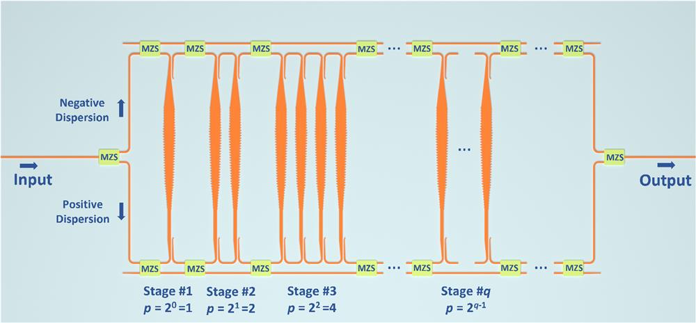
Fig. 1. Schematic diagram of the proposed digital DC consisting of stages of arrayed bidirectional CMWGs which are switched by MZSs.
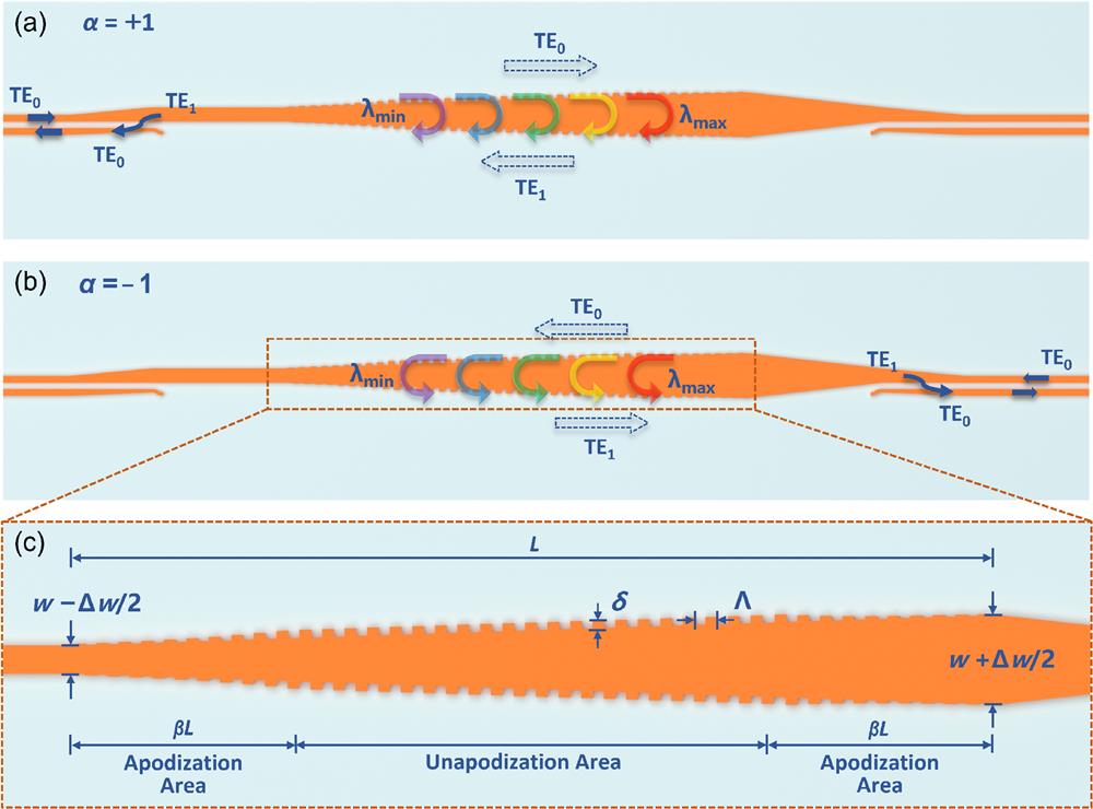
Fig. 2. The present bidirectional CMWG: (a) the operation with positive dispersion (); (b) the operation with negative dispersion (); and (c) structural parameters.
Fig. 3. Simulated responses for the CMWG with different apodization length ratios . (a) Transmission spectrum; (b) group delay spectrum; (c) group delay spectrum at 1540 to 1545 nm; (d) group delay spectra with linear data fitting; and (e) average GDR variation as the apodization length ratio varies.
Fig. 4. Simulated results for the DC operating with positive or negative dispersion as the total number of the involved CMWGs increases. Calculated transmissions for the case with (a) positive or (b) negative dispersions. Calculated group delay for the case with (c) positive or (d) negative dispersions. (e) The dispersion-tuning range as the CMWG number increases.
Fig. 5. Microscope images of the fabricated DC: (a) full view of the DC; zoom-in view of the (b) input coupler, (c) the MZS, (d) the region for positive dispersion-tuning, and (e) the region for negative dispersion-tuning. GC, grating coupler; EC, edge coupler.
Fig. 6. Measured transmissions of the fabricated devices. (a) Measured transmission for a pair of mode (de)multiplexers. (b) Measured transmissions at the cross/bar ports of the MZS at the OFF/ON states. (c) Measured spectral responses when selecting a single CMWG () at different temperatures. Measured transmission of the present DC operating with (d) positive dispersion and (e) negative dispersion when different numbers of CMWGs are involved.
Fig. 7. Measured group-delay and dispersion of the fabricated DC. (a) Measured (circles) and linearly fitted (dashed lines) group-delay by switching the and MZSs at the input/output ports and all the MZSs. (b) Measured dispersion as the number of the CMWGs involved increases. Measured group delay of the DC operating with (c) positive dispersion and (d) negative dispersion at different wavelengths for the case of .
Fig. 8. Experimental setup for the measurement of the group delay and the dispersion. TLS, tunable laser source; PC, polarization controller; IM, intensity modulator; EDFA, erbium-doped fiber amplifier; SCG, synthesized clock generator; and DCA, digital communication analyzer.
Structure | Platform | Circulator-free | Dispersion tunable | Delay range (ps) | Bandwidth (nm) | Loss (dB/ns) | Dispersion (ps/nm) | Footprint () | Contra-DC6 | Silicon | √ | — | 400 | 12 | 25.4 | 33 | ∼6.86 × 0.57 | Spiral Bragg32 | Silicon | — | — | 628 | 22.5 | 6 | −27.7 | 0.3 × 0.3 | Spiral Bragg46 | Silicon nitride | — | — | 1440 | 9.2 | 1.875 | −156.5 | 2.8 × 2.8 | Multimode spiral Bragg33 | Silicon nitride | √ | — | 2864 | 23 | 1.57 | 158 | 2 × 2 | MRRs22 | Silicon nitride | √ | √ | 560 | 0.064 | — | — | 5.5 × 16 | MZIs25 | Silicon nitride | √ | √ | — | 0.8 | — | −550 to 550 | 9.89 × 22.5 | Cascaded CMWG35 | Silicon | √ | √ | 760 | 20 | 10.53 | 0 to 42.8 | 2.4 × 0.38 | This work | Silicon | √ | √ | 2058 | 20 | 11.71 | −61.53 to 63.77 | 5 × 0.38 |
|
Table 1. Summary of reported on-chip DCs.