1Zhejiang University, College of Optical Science and Engineering, International Research Center for Advanced Photonics, State Key Laboratory for Extreme Photonics and Instrumentation, Hangzhou, China
2Jiaxing Key Laboratory of Photonic Sensing and Intelligent Imaging, Jiaxing, China
3Zhejiang University, Jiaxing Research Institute, Intelligent Optics and Photonics Research Center, Jiaxing, China
4Zhejiang University, Ningbo Research Institute, Ningbo, China
A silicon-based digitally tunable positive/negative dispersion controller (DC) is proposed and realized for the first time using the cascaded bidirectional chirped multimode waveguide gratings (CMWGs), achieving positive and negative dispersion by switching the light propagation direction. A 1 × 2 Mach–Zehnder switch (MZS) and a 2 × 1 MZS are placed before and after to route the light path for realizing positive/negative switching. The device has Q stages of identical bidirectional CMWGs with a binary sequence. Thus the digital tuning is convenient and scalable, and the total dispersion accumulated by all the stages can be tuned digitally from - ( 2Q - 1 ) D0 to ( 2Q - 1 ) D0 with a step of D0 by controlling the switching states of all 2 × 2 MZSs, where D0 is the dispersion provided by a single bidirectional CMWG unit. Finally, a digitally tunable positive/negative DC with Q = 4 is designed and fabricated. These CMWGs are designed with a 4-mm-long grating section, enabling the dispersion D0 of about 4.16 ps / nm in a 20-nm-wide bandwidth. The dispersion is tuned from -61.53 to 63.77 ps / nm by switching all MZSs appropriately, and the corresponding group delay is varied from -1021 to 1037 ps.
Dispersion controllers (DCs) are vital for a wide variety of optical systems, including optical communications and microwave photonics.1 In particular, dispersion tunability is highly demanded to realize flexible and intelligent system management. For example, DCs help preserve the signal integrity by counteracting the pulse broadening and distortion due to the accumulated dispersion during the long-haul propagation, facilitating high-quality data transmission.2,3 For microwave photonics, DCs also serve as one of the key fundamental components for controlling the time delay.4,5 Particularly, precise dispersion management enables the realization of optical true time delay lines across a broad frequency range, which is attractive for the realization of phased array antennas and beamforming.6,7 Also dispersive propagation-based arbitrary waveform generation is essential for pulse shaping and frequency-to-time mapping,8,9 whereas group-velocity dispersion management is frequently engineered to maximize the efficiency of higher-order nonlinear effects.10,11 As a result, DCs often play a vital role in manipulating the temporal and spectral properties of optical pulses. For example, it is essential to achieve ultrashort and high-intensity pulses for nonlinear photonics, including optical parametric amplification,12 supercontinuum generation,13 soliton generation,14 and pulse compression.15 Furthermore, reconfigurable dispersion controlling also enables the generation of quantum transforms, showing great potential as a promising technology for future photonic quantum data-locking applications.16,17
For the sake of footprint compactness and massive producibility, on-chip DCs have attracted intensive attention in recent years, and great progress has been achieved with various photonic waveguides and structures.18–20 Among them, as it is well known, silicon photonics has gained prominence because of its high integration density and complementary-metal-oxide-semiconductor compatibility.21 Generally speaking, dispersion control is often realized by manipulating the group velocity. In the past years, various silicon-based on-chip DCs have been developed using the structures, such as microring resonators (MRRs),22,23 Mach–Zehnder interferometers (MZIs),24,25 and waveguide Bragg gratings.26 When using MZIs in cascade, DCs with continuously adjustable dispersion can be realized by adjusting the length difference between the two arms, simultaneously enabling the wavelength-division-multiplexing and the true time delay.27 Nonetheless, such MZI-based DCs suffer from large footprints and highly narrow bandwidths (e.g., ).24 DCs can also be realized with MRRs, providing compact sizes and flexible tunability by controlling the coupling coefficients. As shown in Ref. 28, the maximal dispersion is as high as , but its bandwidth is even . In addition, critical thermal tuning is necessary for the DCs based on MZIs and MRRs for precise dispersion management. In pursuit of high-dynamics dispersion controlling, chirped Bragg gratings have been proposed by introducing a refractive index profile varied gradually along the propagating direction, which produces continuous wavelength-dependent delay variations.29 However, when using those traditional singlemode Bragg gratings, one often has to introduce an optical circulator to separate the reflected light from the input port, which is challenging to be integrated monolithically. Alternatively, contra-directional couplers (contra-DCs) have been proposed with the ability to drop the reflected signals by consisting of two strip waveguides with grating corrugations in between. In Ref. 6, a maximal group delay of 400 ps and a fixed dispersion value up to have been achieved using the contra-DC assisted by an integrated reflector. However, such a structure with two tapered strip waveguides with a shallow slot and grating corrugations in between is quite complex, which thus hinders further improvements for the applications.
Hence, chirped multimode waveguide gratings (CMWGs) have been proposed as a promising option by introducing a structure consisting of a single-waveguide grating assisted with a mode (de)multiplexer because of the circulator-free operation and the simple structural design,30,31 which facilitates high scalability and monolithic-integration convenience. For the single-waveguide grating structure for substantial dispersion, a compact footprint is still achieved easily using a spiral architecture.32,33 Alternatively, utilization of straight CMWGs in cascade provides a very attractive solution for achieving sufficiently high dispersion within a minimized footprint.34 Moreover, it is also very promising to realize digital dispersion-tuning with the assistance of multiple stages of Mach–Zehnder switches (MZSs). As presented in Ref. 35, we have proposed and demonstrated an on-chip digitally tunable DC for the first time using CMWGs, which exhibits wide-range dispersion tuning within a bandwidth of 20 nm.
Sign up for Advanced Photonics TOC. Get the latest issue of Advanced Photonics delivered right to you!Sign up now
Note that positive/negative dispersion tuning is highly desired for applications, such as microwave photonic filters and arbitrary waveform generation.19 For example, the delay tuning range can be doubled even without notably introducing complexity for the systems, which is helpful for the applications, such as optical phase arrays and beam forming.20 Also positive/negative dispersion tuning provides improved flexibility and adaptability for the systems when facing random phase and delay disorders.36 In Ref. 25, a DC consisting of cascaded MZIs was realized with silicon-nitride optical waveguides, producing an extensive tuning range of to , providing a solid dispersion compensation ability for high-speed communication systems. However, the operation bandwidth is very limited to no more than 0.8 nm, even with a very large footprint of . Thus a compact on-chip positive/negative DC with a broad bandwidth is highly required to meet the demands of high-capacity and low-loss modern optical systems with multiple channels.
Here we propose a digitally tunable positive/negative DC for the first time by introducing novel bidirectional CMWGs. The bidirectional CMWGs introduced here are capable of providing positive and negative dispersion, which depends on the light propagation direction in them. In addition, a optical switch is used at the input side for routing the input light to the target port of a bidirectional CMWG, in which way positive or negative dispersion can be realized freely. Another optical switch is added at the output side to route the light propagating bidirectionally to the same output port. Utilization of the CMWG technology enables the separation of the light reflected by the grating from the input port even without any circulator, making it convenient to be used and scaled for applications in systems.37 For the present digitally tunable positive/negative DC, there are stages of bidirectional CMWGs and MZSs integrated monolithically on silicon. All these CMWGs are designed identically to make the chip design convenient and scalable, whereas the number of the CMWGs in cascade for the ’th stage is given by . As a result, the total dispersion for the present positive/negative DC is accumulated by all the stages, which can be tuned digitally by controlling the switching states of all MZSs. Since there are bidirectional CMWGs involved totally, the accumulated dispersion can be freely tuned from to with a step of , where is the dispersion provided by a single bidirectional CMWG unit. As an example, a digitally tunable positive/negative DC with is designed and fabricated by integrating four stages of bidirectional CMWGs and MZSs. The footprint of the present chip is . Here the CMWGs are with a 4-mm-long grating section, enabling the dispersion of about in a 20-nm-wide bandwidth. Accordingly, the dispersion can be tuned from to by switching the , , and MZSs, appropriately. Accordingly, the maximum group delay is varied from to 1037 ps, and the tuning range of the normalized dispersion is from to within a 20-nm-wide bandwidth.
2 Results
2.1 Structure, Principle, and Design
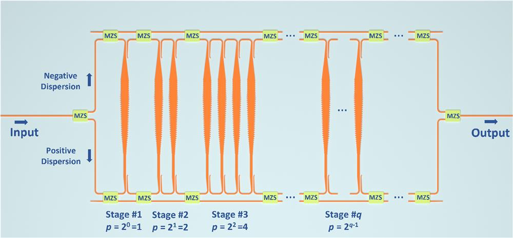
Figure 1 shows the schematic configuration of the proposed digital DC consisting of stages of arrayed bidirectional CMWGs, which are switched by multiple MZSs. The bidirectional CMWGs introduced here can provide positive or negative dispersion, depending on the direction of light propagating in them. For ease of scalability, all the bidirectional CMWGs are designed identically with the same dispersion, denoted as , while the sign of dispersion unit can be switched by selecting the input port. Here a optical switch is placed at the input side for switching the input light to the target port of a bidirectional CMWG, in which way positive or negative dispersion is realized freely. Another optical switch is added at the output side to route the light propagating bidirectionally to the same output port. Hence, the fixed dispersion step for any bidirectional CMWG is given as , where for positive dispersion and for negative dispersion.
Figure 1.Schematic diagram of the proposed digital DC consisting of stages of arrayed bidirectional CMWGs which are switched by MZSs.
For the proposed digitally tunable DC, there are identical bidirectional CMWGs in cascade at the ’th stage, and the number is given by
As a result, the total number of the CMWGs included in the DC is given as . To achieve digital dispersion-tuning, thermo-optic MZSs with low random phase errors, as proposed in our previous work,38 are utilized at each stage. By switching the MZSs appropriately, the number of the CMWGs involved for the dispersion accumulation is given by where denotes the state of the MZS at the ’th stage, and one, respectively, has and 1 for the OFF and ON states. The accumulated dispersion by the DC is then given by
With this structure, the dispersion can be digitally tuned from to with a tuning step of , enabling a large dispersion tuning range of .
As a key component of the DC, the CMWG is designed with asymmetric grating corrugations, which enables the conversion from the forward mode to the reflected mode backward according to the coupled-mode theory.39 Particularly, the grating is chirped by gradually varying the waveguide widths along the lengthwise direction to make the light reflected at different positions depending on the operation wavelength. Since the effective indices of the and modes in the waveguide are proportional to the waveguide core width, one has a shorter-wavelength light reflection at the position with a narrower core width. As a result, when light is input from the port with a narrow core, one has positive dispersion [see Fig. 2(a)]. Otherwise, when light is input from the other port with a wide core, one has negative dispersion [see Fig. 2(b)]. The reflected mode is then dropped to the mode at the drop port with high efficiency and low crosstalk by utilizing a mode (de)multiplexer. This combination of the bidirectional CMWG and the mode (de)multiplexers eliminates the need for optical circulators, whose monolithic integration is still very challenging.40 In this paper, the mode (de)multiplexers are designed with an adiabatic dual-core taper waveguide41 whose widths are chosen optimally according to the dispersion curves of silicon photonic waveguides with a 220-nm-thick top-silicon layer (), a buffer silica cladding (), and an upper silica cladding.
Figure 2.The present bidirectional CMWG: (a) the operation with positive dispersion (); (b) the operation with negative dispersion (); and (c) structural parameters.
The conversion from the forward mode to the backward mode is realized by choosing the grating period according to the Bragg condition: where is the reflected Bragg wavelength, is the grating period, and and are the effective refractive indices of the and modes, respectively. To make the grating chirped precisely, the core width in the grating section is linearly varied while the period is fixed.42 As shown in Fig. 2(c), the central core width of the bidirectional CMWG component is gradually tapered from to along the lengthwise direction, where is the core width at the middle of the grating section. Regarding that the propagation loss for the modes is mainly from the sidewall scattering, here a relatively large central width is chosen as , so that the electric intensity at the sidewalls is reduced greatly to lower the propagation loss possibly. Accordingly, the grating period is chosen as 284 nm by following Eq. (4). On the other hand, a weak grating is preferred to minimize the loss of light propagating along the grating by introducing shallow corrugation depth . For example, the maximal corrugation depth is chosen as 150 nm, regarding the fabrication limitation. Even though a weak grating is used, light can still be fully reflected if the grating is long enough (e.g., with a length of ). For such a CMWG, the bandwidth is mainly determined by the core-width variation , and the maximal group delay depends on the given grating length. When choosing a large core-width variation , the dispersion becomes low. Therefore, the core-width variation must be selected carefully to provide a sufficient bandwidth for large dispersion. In this paper, we choose according to the requirements. Furthermore, in order to reduce the group delay ripples (GDRs) due to the Fabry–Perot resonance resulting from the reflection at the transition between straight and grating sections,43 the corrugation depth is gradually varied from 0 to at both two ends of the bidirectional CMWG by following the apodization function: where is the total grating length, and is the apodization length ratio.
Figures 3(a) and 3(b) show the calculated results of the transmission spectral responses and the group delays using the transfer matrix method.44 Here the propagation loss is reasonably assumed to be according to the experimental results, and the apodization length ratio is chosen as 0, , , , and , respectively. As shown in Fig. 3(a), the bandwidth is shrunken slightly from 25 to 18 nm when increases from 0 to 1/2, and the transmissions within the bandwidth are kept to be low loss. From Fig. 3(b), it can be seen that there are notable ripples as large as when (i.e., no apodization is introduced), while the ripples are well suppressed as increases. More details in the wavelength range of 1540 to 1545 nm are given in Figs. 3(c) and 3(d). When increases to be more than , the ripples become almost zero in the wavelength band of 1540 to 1545 nm, as shown in Fig. 3(d). On the other hand, it is often desired to achieve the group delay varied linearly as the wavelength increases. From Fig. 3(d), it can be seen that the linearity becomes worse when the grating is fully apodized (i.e., ).45Figure 3(e) shows the calculated average GDR as increases from 0 to 1/2. Here the average GDR is defined as the averaged deviation between the simulated value of the group delay and the target value fitted linearly.46 As it can be seen, one has a GDR of , , , , and , respectively, when , , , , and 1/2. Here we choose for achieving low ripples of as well as high linearity in the wavelength range 1532 to 1548 nm. As a result, for the designed bidirectional CMWG, the 3-dB bandwidth is about 23.7 nm, the maximal group delay is 115 ps, and the dispersion is about . On the other hand, a negative dispersion of is produced when light is input from the other end with wide core.
Figure 3.Simulated responses for the CMWG with different apodization length ratios . (a) Transmission spectrum; (b) group delay spectrum; (c) group delay spectrum at 1540 to 1545 nm; (d) group delay spectra with linear data fitting; and (e) average GDR variation as the apodization length ratio varies.
The digital dispersion tuning is achieved by appropriately switching the MZSs that are designed according to our previous work.38 Here we consider the DC with four stages (i.e., ), regarding the limitation due to the loss issue in experiments. According to the structure shown in Fig. 1, there are 15 CMWGs available at maximum. Figures 4(a)–4(d) show the transmission and the group delay of the DC operating with positive or negative dispersion as the total number of the involved CMWGs increases. When the DC operates with positive dispersion, the longer wavelength experiences a longer propagation distance, and thus a higher excess loss, as shown in Fig. 4(a). In contrast, when the DC operates with negative dispersion, the longer wavelength experiences a shorter propagation distance, and thus a lower excess loss, as shown in Fig. 4(b). Since the maximal propagation distance for the longest wavelength with the maximal positive dispersion is about 12 cm, the longest wavelength shows the maximal delay of 1736 ps and the highest total loss of about 12 dB as the propagation loss is assumed to be here, as shown in Figs. 4(a) and 4(c). Similarly, when operating with negative dispersion, the shortest wavelength has the maximal delay of 1663 ps and the highest total loss of about 12 dB [see Figs. 4(b) and 4(d)]. In this case, the designed DC enables digital dispersion tuning from to with a step of 6.30 and for positive and negative dispersions, respectively, as shown in Fig. 4(e). Correspondingly, the total dispersion-tuning range is , and the total delay tuning range reaches 3399 ps.
Figure 4.Simulated results for the DC operating with positive or negative dispersion as the total number of the involved CMWGs increases. Calculated transmissions for the case with (a) positive or (b) negative dispersions. Calculated group delay for the case with (c) positive or (d) negative dispersions. (e) The dispersion-tuning range as the CMWG number increases.
Note that there is a critical wavelength ( or ) in the CMWG passband defined by , where and are the edge-wavelengths for the passband, as shown in Figs. 4(a)–4(d). For the case of operating with positive dispersion shown in Figs. 4(a) and 4(c), the propagation loss and the group delay increase linearly with the difference when . In contrast, when , the group delay and the propagation loss are kept constant almost, as shown in Figs. 4(a) and 4(c). Similarly, for the case of operating with negative dispersion shown in Figs. 4(b) and 4(d), the propagation loss and the group delay increase linearly with the difference when . In contrast, when , the group delay and the propagation loss are kept constant almost, as shown in Figs. 4(b) and 4(d). This happens for a Bragg grating designed with the core width chirped very slowly.32,47 Here we give an explanation by considering the case of operating with positive dispersion shown in Figs. 4(a) and 4(c) as an example. For the present CMWG, the front-end part is designed with an appropriate period to reflect the wavelength completely within only a few grating periods. Since the chirping of the CMWG is gentle, the wavelength within the range shorter than can still be reflected very well with low losses and accordingly it has a group delay similar to the wavelength . Therefore, one should choose the effective wavelength range as for achieving the positive dispersion, and the wavelength range of should be ignored. Similarly, the effective wavelength range for achieving negative dispersion is given by and the wavelength range of should be ignored.
2.2 Experimental Results
Figure 5 shows the optical microscope image of the fabricated DC, including the zoom-in view of the input couplers, the MZSs, the region for positive dispersion-tuning, and the region for negative dispersion-tuning. The total footprint of the present DC is about . Particularly, the long straight waveguides for connections on the chip are widened to lower the propagation loss greatly.48 For the present DC, there are 12 MZSs in total for the digital dispersion tuning. Among them, MZSs S02 to S06 and MZSs S08 to S12 are used for the cases with positive and negative dispersions, respectively. Meanwhile, MZSs S01 and S07 are used to switch at the input/output ports to achieve positive/negative dispersion.
Figure 5.Microscope images of the fabricated DC: (a) full view of the DC; zoom-in view of the (b) input coupler, (c) the MZS, (d) the region for positive dispersion-tuning, and (e) the region for negative dispersion-tuning. GC, grating coupler; EC, edge coupler.
Figure 6(a) shows the measured transmission spectrum of a pair of mode (de)multiplexers, and Fig. 6(b) shows the measured transmission spectrum of the cross/bar ports of an MZS at the OFF/ON states. These results are normalized with the transmission of a straight single-mode silicon photonic waveguide fabricated on the same chip. From Fig. 6(a), it can be seen that the fabricated mode (de)multiplexer has an excess loss of and intermode crosstalk of in the wavelength range of 1525 to 1560 nm, as expected in theory. It is crucial to achieve high extinction ratios for MZS used in system so that the crosstalk can be minimized. Fortunately, the measurement results given in Fig. 6(b) show that the MZS works very well with high performances, exhibiting a low excess loss of and a high extinction ratio of for both OFF and ON states. In addition, the applied voltage is when operating at the ON state, and the thermal-optic switching speed is around microseconds, which is similar to the results for silicon photonic devices reported previously.49Figure 6(c) shows the measured spectral responses for a single CMWG () as the temperature varies from 27°C to 87°C. It can be seen that the center wavelength is red-shifted linearly with a slope of , and the measured group-delay response has the same redshifts as well. As a result, the working temperature should be stabilized to avoid any random variation. On the other hand, it is possible to achieve fine tuning of the group-delay thermally. Figures 6(d) and 6(e), respectively, show the measured transmissions of the present DC operating with positive or negative dispersions when different numbers of CMWGs are involved. Here the CMWG number is given as 1, 3, 5, 7, 9, 11, 13, and 15. From the measurement results, the average excess losses for each CMWG are 0.64 and 1.02 dB within the wavelength bandwidth of 20 nm for positive and negative dispersion, respectively. When all CMWGs are involved (i.e., ), the measured propagation loss varies from 9.39 dB at 1530.2 nm to 25.28 dB at 1546.9 nm for the case with positive dispersion and from 23.48 dB at 1530.7 nm to 15.21 dB at 1547 nm for the case with negative dispersion, respectively. The difference between the two cases with positive and negative dispersions is due to that the mode (de)multiplexers have larger excess losses at longer wavelengths [shown in Fig. 6(a)]. The power fluctuations at 1531.5 and 1544 nm are mainly due to the field stitching of E-beam writing and related fabrication errors, which can be lowered greatly if the fabrication processes are improved. Moreover, the fluctuation accumulates as the number of the CMWGs in cascade increases.
Figure 6.Measured transmissions of the fabricated devices. (a) Measured transmission for a pair of mode (de)multiplexers. (b) Measured transmissions at the cross/bar ports of the MZS at the OFF/ON states. (c) Measured spectral responses when selecting a single CMWG () at different temperatures. Measured transmission of the present DC operating with (d) positive dispersion and (e) negative dispersion when different numbers of CMWGs are involved.
Figure 7(a) shows the measured group-delay spectrum of the present DC (see the data labeled by the circles), providing different group delays from the negative value () to the positive one () by switching the MZSs at the input/output ports and the MZSs for the digital tuning. Here the CMWG number is given as 1, 3, 5, 7, 9, 11, 13, and 15. It can be seen that the group delay increases or decreases linearly as the wavelength increases in the wavelength band of 1532 to 1549 nm. In contrast, the group delay in the wavelength range of 1529 to 1532 nm is insensitive to the wavelength, which is consistent with the theoretical results shown in Fig. 4(c) (see the wavelength range of 1526 to 1532 nm). The measured data in Fig. 7(a) are also fitted linearly, as shown by the dashed lines. Figure 7(b) shows the corresponding positive/negative dispersions as the number of the CMWGs involved increases. The dispersion is digitally tuned from to with a step of , which is produced by each CMWG. When all CMWGs are involved (i.e., ) by turning on all the MZSs, the group delay can be varied from to 1037 ps when switching the MZS at the input side and MZS at the output side, enabling a total group-delay tuning range of 2058 ps. The measured waveforms shown in Figs. 7(c) and 7(d) clearly demonstrate the measured group delay of the DC when operating at different wavelengths of 1532, 1534, …, 1546 nm. The delay loss of the fabricated DC is estimated as 15.32 and for the operations with positive and negative dispersions, respectively.
Figure 7.Measured group-delay and dispersion of the fabricated DC. (a) Measured (circles) and linearly fitted (dashed lines) group-delay by switching the and MZSs at the input/output ports and all the MZSs. (b) Measured dispersion as the number of the CMWGs involved increases. Measured group delay of the DC operating with (c) positive dispersion and (d) negative dispersion at different wavelengths for the case of .
Table 1 gives a summary of the on-chip DCs reported in recent years. It shows that there are very few on-chip DCs enabling positive/negative dispersion. As demonstrated, the DC with continuously adjustable dispersion was realized using cascaded MZIs,24 but it suffers from large footprints and a narrow bandwidth of . In contrast, the present DC has a compact footprint and is the unique one enabling a high positive/negative dispersion within a broad bandwidth of . Furthermore, the present on-chip DC is circulator-free and is flexible to be integrated monolithically with other components, which is very useful for many applications.
In this paper, we have proposed and realized a digitally tunable positive/negative DC for the first time using novel bidirectional CMWGs with dual ports. In particular, a MZS is introduced at the input port, and a MZS is placed at the output side, in which way the on-chip DC can be switched to achieve positive or negative dispersion with the help of the bidirectionality of the CMWGs. The present device consists of MZSs and stages of bidirectional CMWGs designed identically, while bidirectional CMWGs are included for the ’th stage. As a result, the chip design is convenient and scalable. The digital dispersion tuning has been realized with a step of from to by appropriately manipulating the states of all MZSs. An example for a digitally tunable positive/negative DC with has been demonstrated with a compact footprint of , and 15 CMWGs whose grating section is 4 mm long. For the present on-chip DC, the measured dispersion is about in a 20-nm-wide bandwidth, and the total dispersion tuned from to has been achieved by switching all MZSs appropriately, corresponding to the group delay varied from to 1037 ps. As a result, to the best of our knowledge, we have realized the largest group-delay tuning range up to 2058 ps over a 20-nm-wide bandwidth. Furthermore, the present on-chip DC shows very excellent scalability, and a further improvement in the dispersion-tuning range and the loss reduction can be achieved possibly with more stages and better fabrication technologies, which makes it highly versatile for a variety of photonic applications.
4 Appendix: Materials and Methods
4.1 Fabrication
The designed DC was fabricated using a standard process for silicon photonics. The top-silicon layer is 220 nm, and the buried oxide thickness is . A thin-film silica upper cladding was deposited on the top, followed by overlaying a titanium nitride metal heater for thermo-optic MZSs. There is a deep air trench between any two phase-shifters for thermal isolation. The microheaters on the MZSs are connected to the electrical pads via high-conductivity metal lines, and all these electrical pads are wire-bonded to a printed circuit board.
4.2 Experimental Setup
To measure the transmission spectra of the devices on the chip, the setup with a broad-band amplified spontaneous emission light source and an optical spectrum analyzer was used. Moreover, Fig. 8 shows the experimental setup for measuring the group delay and the dispersion. With this setup, light emitted from a tunable laser source (TLS) first goes through a polarization controller (PC) and then an electro-optic (EO) modulator. Here the EO modulator is operated with a 5 to 40 GHz radio frequency signal from a synthesized clock generator. Consequently, the modulated light was amplified with an erbium-doped fiber amplifier (EDFA) and finally was coupled to the on-chip DC. The signal output from the chip was then detected using a digital communication analyzer (DCA). In the experiment, a multichannel voltage source was employed for the operations of MZSs.
Figure 8.Experimental setup for the measurement of the group delay and the dispersion. TLS, tunable laser source; PC, polarization controller; IM, intensity modulator; EDFA, erbium-doped fiber amplifier; SCG, synthesized clock generator; and DCA, digital communication analyzer.
Shujun Liu is a doctoral candidate student at the College of Optical Science and Engineering, Zhejiang University (ZJU), Hangzhou, China. She received her BS degree in optoelectronic information science and engineering from Chongqing University, Chongqing, China. Her current research focuses on the study of integrated optics for dispersion control.
Ruitao Ma is a master candidate student at the College of Optical Science and Engineering, Zhejiang University (ZJU), Hangzhou, China. He received his BS degree in optoelectronic information science and engineering from Nankai University, Tianjin, China. His current research focuses on the study of integrated optics for dispersion control.
Zejie Yu received his BE degree in optical engineering from ZJU and his PhD in electronic engineering from the Chinese University of Hong Kong. Later, he was a postdoctoral scholar in the Department of Electronic Engineering at the Chinese University of Hong Kong. He is currently a tenure-track professor of the College of Optical Science and Engineering at ZJU. His research interests include silicon photonics and heterogeneous integration.
Yaocheng Shi received his PhD from the Royal Institute of Technology (KTH), Stockholm, Sweden, in 2008. Then he joined the College of Optical Science and Engineering at ZJU, where he is a professor. His current research interests include integrated photonics for optical communications, optical interconnections, and optical sensing. He has published about 150 refereed international journal papers and his papers have been cited by more than 6000 times (Google Scholar).
Daoxin Dai received his BEng degree from Zhejiang University (ZJU), China, and his PhD from the Royal Institute of Technology, Sweden, in 2000 and 2005, respectively. Currently, he is the QIUSHI Distinguished Professor at ZJU and is leading the Silicon Integrated Nanophotonics Group. He has published more than 300 international journal papers. He is one of the most cited Chinese researchers (Elsevier) and has given more than 100 plenary/keynote/tutorial/invited talks at prestigious international conferences.