• Laser & Optoelectronics Progress
  • Vol. 59, Issue 3, 0300001 (2022)
Jielian Shen1, Ting Ji1、*, Guohui Li1, Linlin Shi1, Lin Feng1, Wenyan Wang1, Dongdong Li2, and Yanxia Cui1、**
Author Affiliations
  • 1College of Physics and Optoelectronics, Taiyuan University of Technology, Taiyuan , Shanxi 030024, China
  • 2The Interdisciplinary Research Center, Shanghai Advanced Research Institute, Chinese Academy of Sciences, Shanghai 201210, China
  • show less
    DOI: 10.3788/LOP202259.0300001 Cite this Article Set citation alerts
    Jielian Shen, Ting Ji, Guohui Li, Linlin Shi, Lin Feng, Wenyan Wang, Dongdong Li, Yanxia Cui. Through-Hole Anodized Aluminum Oxide Template Assisted Fabrication of Patterned Nanostructures and Their Applications in Optoelectronic Devices[J]. Laser & Optoelectronics Progress, 2022, 59(3): 0300001 Copy Citation Text show less
    Formation mechanisms and structure diagrams for AAO formation based on different models. (a) Field-induced steady-state pore model[19]; (b) critical current density model[22]; (c) expansion of aluminum model[24]; (d) structural diagram of porous AAO film
    Fig. 1. Formation mechanisms and structure diagrams for AAO formation based on different models. (a) Field-induced steady-state pore model[19]; (b) critical current density model[22]; (c) expansion of aluminum model[24]; (d) structural diagram of porous AAO film
    Schematic of AAO template preparation. (a) Schematic for preparation of ultrathin through-hole AAO template by two-step anodization methods; (b) schematic for preparation of through-hole AAO template by nanoimprinting
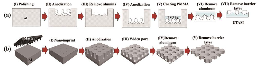
    Fig. 2. Schematic of AAO template preparation. (a) Schematic for preparation of ultrathin through-hole AAO template by two-step anodization methods; (b) schematic for preparation of through-hole AAO template by nanoimprinting
    Schematic for fabricating different nanoparticle with through-hole AAO masks
    Fig. 3. Schematic for fabricating different nanoparticle with through-hole AAO masks
    Schematic for preparation of different nanowire arrays by through-hole AAO template
    Fig. 4. Schematic for preparation of different nanowire arrays by through-hole AAO template
    Schematic for preparation of different nanotube arrays by through-hole AAO template
    Fig. 5. Schematic for preparation of different nanotube arrays by through-hole AAO template
    Solar cells based on AAO template. (a) Anti-reflection principle diagram of AAO nano-grating[84]; (b) comparison of absorption spectra of solar cells with and without nanoparticles[89]; (c) schematic of CdSe nanorods/P3HT solar cell device[94; (d) EQE spectra of the nanorod array devices and the planer structure devices[96]; (e) transient photovoltage decay curves for the nanopillar and planar perovskite-based solar cells[101]; (f) schematic of charge collection with different electron contact in solar cells[104]
    Fig. 6. Solar cells based on AAO template. (a) Anti-reflection principle diagram of AAO nano-grating[84]; (b) comparison of absorption spectra of solar cells with and without nanoparticles[89]; (c) schematic of CdSe nanorods/P3HT solar cell device[94; (d) EQE spectra of the nanorod array devices and the planer structure devices[96]; (e) transient photovoltage decay curves for the nanopillar and planar perovskite-based solar cells[101]; (f) schematic of charge collection with different electron contact in solar cells[104]
    Photodetector based on AAO template. (a) Schematic of the photodetector based on FAPbI3 nanowires embedded in the AAO[116]; (b) Ⅳ curves of the FAPbI3 nanowires[116]; (c) response time of the FAPbI3 nanowires photodetector[116]; (d) mechanism of charge separation and photoresponse activity over CdS/PPV hybrid nanowire arrays[122]; (e) spectral response of the CdS/PPV hybrid nanowire array device[122]; (f) responsivity measurement of the ZnO/NiO composite based photodetector[123]; (g) response spectra of diamond photodetectors with and without Pd[126]; (h) schematic fabrication of the photodetectors based on hybrid plasmonic nanostructure[49]; (i) schematic of the Ge nanodots array/graphene/SiO2/Si photodetector[127]
    Fig. 7. Photodetector based on AAO template. (a) Schematic of the photodetector based on FAPbI3 nanowires embedded in the AAO[116]; (b) Ⅳ curves of the FAPbI3 nanowires[116]; (c) response time of the FAPbI3 nanowires photodetector[116]; (d) mechanism of charge separation and photoresponse activity over CdS/PPV hybrid nanowire arrays[122]; (e) spectral response of the CdS/PPV hybrid nanowire array device[122]; (f) responsivity measurement of the ZnO/NiO composite based photodetector[123]; (g) response spectra of diamond photodetectors with and without Pd[126]; (h) schematic fabrication of the photodetectors based on hybrid plasmonic nanostructure[49]; (i) schematic of the Ge nanodots array/graphene/SiO2/Si photodetector[127]
    LED based on AAO template. (a) Photonic crystal structures on the surfaces of GaN-based LED[134]; (b) PL spectra of nanostructured LEDs of different depths[135]; (c) voltage-current-light output curves of conventional LEDs and surface patterned LEDs[136]; (d) device structure of LED based on nanocomb-shaped PSS[139]; (e) light racing schematic diagram of BP-LED and HP-LED[140]; (f) far-field radiation patterns of BP-LED and HP-LED[140]; (g) UV-Visible absorption spectra of the CsPbI3 nanowire films at different storage times[141]; (h) structure diagram of perovskite nanowire LED device[142]; (i) mechanical robustness test of nanowire and thin film devices after certain bending cycles[142]
    Fig. 8. LED based on AAO template. (a) Photonic crystal structures on the surfaces of GaN-based LED[134]; (b) PL spectra of nanostructured LEDs of different depths[135]; (c) voltage-current-light output curves of conventional LEDs and surface patterned LEDs[136]; (d) device structure of LED based on nanocomb-shaped PSS[139]; (e) light racing schematic diagram of BP-LED and HP-LED[140]; (f) far-field radiation patterns of BP-LED and HP-LED[140]; (g) UV-Visible absorption spectra of the CsPbI3 nanowire films at different storage times[141]; (h) structure diagram of perovskite nanowire LED device[142]; (i) mechanical robustness test of nanowire and thin film devices after certain bending cycles[142]
    Device structureResponse time /msRecovery time /msDetectivity/JonesWavelength /nmBias voltage /VReference
    ITO/MAPbI3 nanowire array/Au20.4713.811.00×10100.3118
    ITO/CsPbI3 nanowire array/Au292.00234.001.57×1085.0115
    Al/CH3NH3SnI3 nanowire array/Au1500.00400.008.80×10102.0119
    ITO/FAPbI3 nanowire array/Al8.509.502.00×1011-5.00×10114507.0116
    ITO/MAPbI3 quantum wires/Al80.00140.00--5.0120
    Table 1. Performance of perovskite nanowire photodetectors based on through-hole AAO template
    NanostructureTechnologyCurrent /mALight output power improved /%Reference
    GaN nanoholeICP2011.3135
    SiO2 nanoholeICP2019.0136
    ITO+GaN nanoholeICP2049.7133
    SiO2+ITO nanoholeICP3507.0128
    ITO+GaN nanoholeRIE2094.0134
    ITO nanoholeICP-RIE2072.0132
    Table 2. Performance of LED devices with surface nanostructures prepared by AAO mask
    Jielian Shen, Ting Ji, Guohui Li, Linlin Shi, Lin Feng, Wenyan Wang, Dongdong Li, Yanxia Cui. Through-Hole Anodized Aluminum Oxide Template Assisted Fabrication of Patterned Nanostructures and Their Applications in Optoelectronic Devices[J]. Laser & Optoelectronics Progress, 2022, 59(3): 0300001
    Download Citation