
Kun Gao, Xiangyu Cao, Jun Gao, Tong Li, Huanhuan Yang, Sijia Li, "Ultrawideband metamaterial absorber for oblique incidence using characteristic mode analysis," Photonics Res. 10, 2751 (2022)
- Photonics Research
- Vol. 10, Issue 12, 2751 (2022)
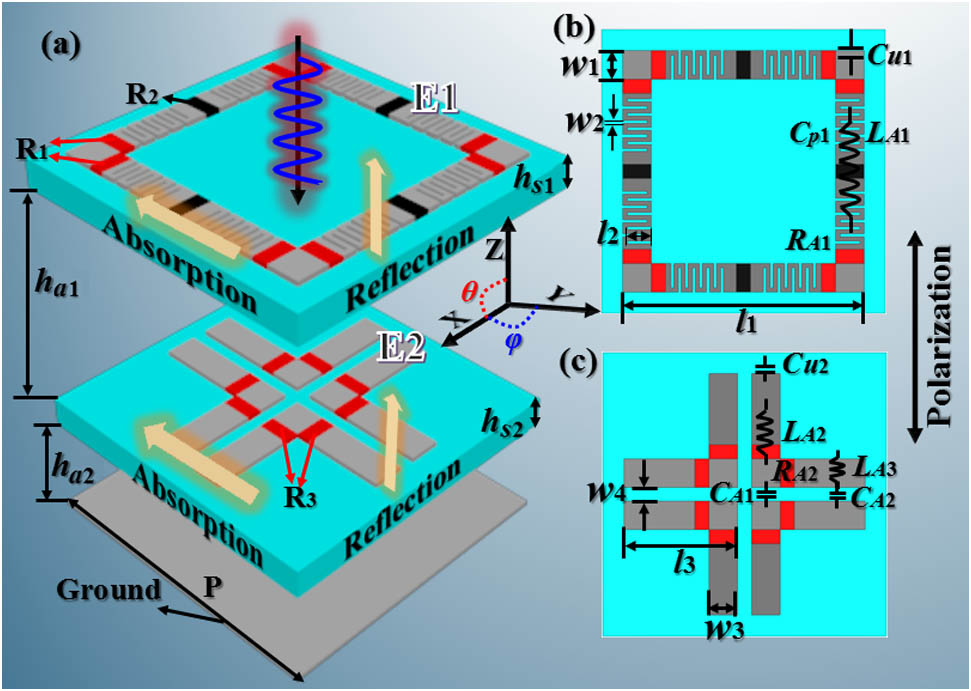
Fig. 1. Topology and dimensions of the proposed metamaterial absorber. (a) Three-dimensional perspective. (b) Top square meander loop embedded with lumped resistors (E1). (c) Middle bent metallic strips embedded with lumped resistors (E2). P = 10 mm l 1 = 8.5 mm w 1 = 1 mm l 2 = 0.85 mm w 2 = 0.1 mm l 3 = 4 mm w 3 = 1 mm w 4 = 0.5 mm h s 1 = 0.72 mm h s 2 = 0.79 mm h a 1 = 3.8 mm h a 2 = 1.5 mm
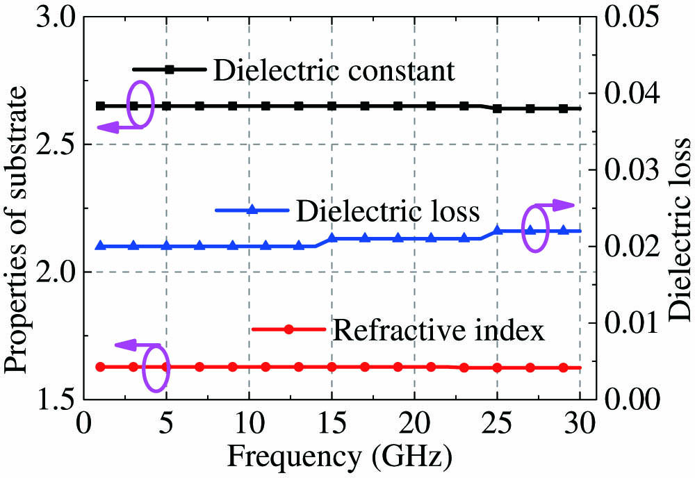
Fig. 2. Properties of substrate.
Fig. 3. Modal currents and modal radiation patterns. (a) and (b) Element 1 without lumped resistors and meander lines. (c) and (d) Element 2 without resistors.
Fig. 4. Modal significances: (a) Element 1 and (b) Element 2 without resistors. Characteristic angles: (c) Element 1 and (d) Element 2 without resistors.
Fig. 5. Modal significances: (a) Element 1 and (b) Element 2 with resistors. Characteristic angles: (c) Element 1 and (d) Element 2 with resistors.
Fig. 6. MWC of Element 1 and Element 2 without resistors at oblique angle of incidence. Element 1 under (a) TE and (c) TM polarization. Element 2 under (b) TE and (d) TM polarization.
Fig. 7. (a) Equivalent circuit of the proposed absorber. (b) Reflection coefficient of simulation and equivalent circuit model. (c) Admittance Smith chart.
Fig. 8. Simulated absorption variation with incidence angle, for (a) TE and (b) TM polarizations. RCS reduction between the proposed absorber and ground, for (c) TE and (d) TM polarizations.
Fig. 9. Fabricated prototypes of absorber array. (a) 3D perspective. (b) Measurement environment. (c) Top layer. (d) Middle layer.
Fig. 10. Simulated and measured absorption for (a) TE polarization and (b) TM polarization.
|
Table 1. Performance Comparison between the Proposed and Reported Absorbers


Set citation alerts for the article
Please enter your email address

© Copyright 2018-2021 | Chinese Laser Press. All Rights Reserved 沪ICP备15018463号-20