An ultrawideband, polarization-insensitive, metamaterial absorber for oblique angle of incidence is presented using characteristic mode analysis. The absorber consists of conductive meander square loops and symmetric bent metallic strips, which are embedded with lumped resistors. With the aid of modal currents and modal weighting coefficients, the positions of the lumped resistors are determined. After that, the equivalent circuit (EC) model and admittance formula are proposed and analyzed to further understand the working principle and ultrawide bandwidth. The proposed absorber measures an absorption bandwidth of 4.3–26.5 GHz (144.1% in fractional bandwidth) for 90% absorptivity under normal incidence. At the oblique angle of incidence of 45°, the bandwidth of 90% absorptivity is still 5.1–21.3 GHz (122.72%) for transverse electric (TE) polarization, and 6.8–29.5 GHz (125.07%) for transverse magnetic (TM) polarization. The good agreement among simulation, measurement, and EC calculation demonstrates the validity of the proposed method and indicates that the method can be applied to other microwave and optical frequency bands. The proposed metamaterial absorber can be widely applied in electromagnetic compatibility, electromagnetic interference, radar stealth, and biomedical detection.
1. INTRODUCTION
The development of electromagnetic (EM) metamaterials provides a broad prospect for manipulating the polarization, amplitude, and phase of electromagnetic waves to achieve multifunctionality [1,2]. Metamaterial absorbers (MMA) are widely used in various fields due to their unique characteristics, such as radar stealth [3,4], electromagnetic interference [5], wireless communication [6], imaging systems [7], and biomedical detection [8,9]. Salisbury screen [10], Jaumann absorber [11], and perfect metamaterial absorber [12], as early successful practices, although limited by narrow bandwidth and relatively large thickness, also explored a feasible technical route for metamaterial absorbers design.
The bandwidth, oblique angle of incidence and profile thickness of MMAs are a pair of contradictions that are difficult to reconcile. Therefore, an appropriate compromise should be taken to achieve satisfactory performance. The introduction of circuit analog absorbers is an excellent scheme, which greatly addresses the above limitations [13]. At the same time, equivalent circuit (EC) theory is also a rapid and effective method to guide the design of wideband and low-profile circuit analog absorbers [14–18]. In Ref. [15], the proposed absorber was composed of a lossy layer and four rotationally symmetric bent metallic strips embedded with two chip resistors. The metallic strips embedded with the resistors generated three resonant modes, and the current was consumed through the chip resistor in different modes. A quasi-single-layer circuit analog absorber was proposed in Ref. [16], with two square loop arrays embedded with lumped elements printed on the top and bottom of the lossy dielectric. In Ref. [17], the usage intercalated few-layer graphene for the development of an optically tunable absorbing metasurface is proposed. The geometrical parameters of the metasurface are optimized using the EC theory, which achieves an optically controllable absorption in terahertz imaging and photodetection. The introduction of equivalent circuit, input impedance, and current distribution provided great insight into the existence of resonance and broadband. In addition, indium tin oxide [19,20], water [21,22], and graphene [23,24] are also applied to develop metamaterial absorption.
However, most of the research in the literature only focuses on the normal incidence, while the absorption for the oblique angle of incidence urgently needs principal insight and practical application [25–27]. In Ref. [26], a dual-section step-impedance frequency selective surface (DSSI-FSS) absorber was developed for oblique incidence applications, and a transmission line model was proposed for DSSI-FSS absorbers at different incidence angles. It exhibited stable absorption properties for both TE and TM polarizations at incident angles from 0° to 45°. In Ref. [27], a novel absorber was proposed, which consists of a conductive square loop array embedded with lumped resistors and a wide-angle impedance matching (WAIM) layer. Equivalent circuit and rigorous formula derivations are introduced to gain insight into the deterioration of absorption performance under oblique incidence and effect of the WAIM layer. At an incident angle of 45°, the overlapped bandwidth for TE and TM polarizations is still 110.5%.
It is worth mentioning that the equivalent circuit is incapable of designing complex structures, and the guidance of oblique angle of incidence requires rich experience. The source-free characteristic mode theory (CMT) defines a set of mutually orthogonal modal currents, which provides profound physical insights for the analysis and modification of fundamental mode and higher-order modes [28–30]. It has successfully guided the design of metasurface antennas [31–36] and has been applied in the field of microwave absorption [19,37–41]. In Ref. [35], the CMT based on the surface integral equation formalism is proposed for the analysis of plasmonic nanostructures, which can be utilized in the design and tuning of nanoantenna configurations for specific application. Reference [36] demonstrates the value of CMA-based design insights for antenna engineering and looks forward to new research directions for CMA and antenna research. In Ref. [37], a multimode and broadband absorber was proposed using characteristic mode analysis (CMA), and the underlying modal behavior of the absorber was analyzed to guide the design. In Ref. [38], with the aid of the characteristic modes and characteristic currents, the value of loading resistance could be determined. The equivalent impedance and surface current distribution of the absorber were analyzed to study its working mechanism. The successful practice of CMA provides a reference for microwave absorption. To the authors’ knowledge, CMA has not yet investigated the metamaterial absorber for oblique angle of incidence.
In this study, a novel ultrawideband, polarization-independent metamaterial absorber for oblique angle of incidence is proposed. The positions of the lumped resistors are determined using the modal field and modal parameters. The EC and admittance formula are analyzed to further understand the working mechanism and ultrawide bandwidth. The proposed absorber achieves a fractional bandwidth of 144.1% for 90% absorptivity under normal incidence. At the oblique angle of incidence of 45°, the bandwidth of 90% absorptivity still reaches four octaves for TE and TM polarizations. The simulation, measurement, and EC calculation demonstrate the effectiveness and reliability of the proposed method; it is also worth pointing out that the method can be extended to other microwave and optical fields.
2. DESIGN AND ANALYSIS OF THE PROPOSED METAMATERIAL ABSORBER
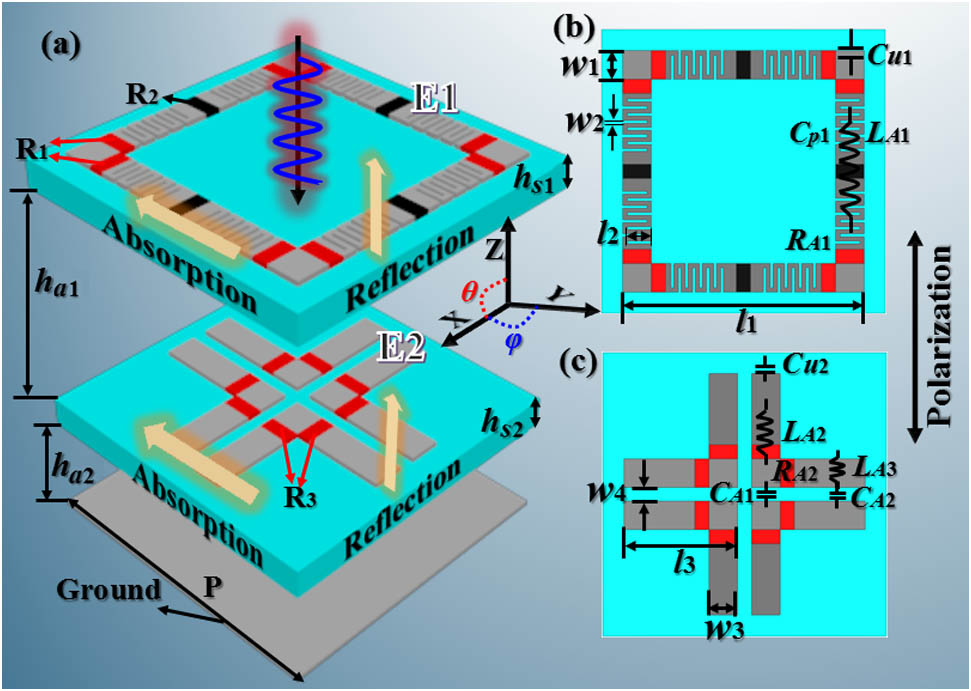
Figure 1 shows the schematic of the metamaterial absorber structure with an element size of , including two lossy layers and a bottom metal ground. The upper structure adopts a conductive meandering square loop (E1), and lumped resistors (marked in red) and (marked in black) are embedded in the right-angled corners and the middle of the square loop, respectively. The middle structure employs four symmetrically placed bent metallic strips embedded (E2) with lumped resistor (marked in red) at right-angled corners. The thicknesses of two layers of dielectric substrates are and , respectively, and each layer is filled with air of thickness and , respectively. As shown in Fig. 2, the dielectric constant of the substrate material is 2.65, and, at frequencies above 25 GHz, the dielectric constant is 2.64, which remains stable overall. The dielectric loss is 0.02; at high frequencies, the loss increases slightly. The expression of refractive index is . Therefore, the refractive index of the substrate material is 1.628 and 1.625 for frequencies above 25 GHz. When the dielectric loss increases, the transmittance decreases and the reflectance increases.
Figure 1.Topology and dimensions of the proposed metamaterial absorber. (a) Three-dimensional perspective. (b) Top square meander loop embedded with lumped resistors (E1). (c) Middle bent metallic strips embedded with lumped resistors (E2). , , , , , , , , , , , and .
A. Characteristic Mode Analysis and Design of the Absorber
From the characteristic mode theory based on the method of moment (MOM), the radiation and scattering properties of dielectric materials can be clearly obtained [28–30]. The total current on the conductive surface of different elements can be expressed as a linearly weighted superposition of a series of mutually orthogonal characteristic modes (CMs): where is the modal weighting coefficient (MWC) of the th modal current, representing the contribution of each to the total radiated power. The modal weighting coefficient is related to the external electric field and modal current, which is defined as where the numerator is called the modal excitation coefficient. The modal significance (MS) is only related to eigenvalues, expressed as
The eigenvalue has a large variation range, while the range of MS is [0, 1]. When the value of MS is close to zero, it indicates that the mode is in resonance. If the value of MS is greater than 0.707, it indicates that the mode is an effective mode, which can be effectively excited under appropriate circumstances. For the absorber, the absorption bandwidth is in the range of MS value greater than 0.707.
The characteristic angle (CA) is expressed as
The modes are presented as capacitive for characteristic angles greater than 180° and, on the contrary, exhibit inductance. CMs are obtained using the MOM-based characteristic mode analysis tool in computer simulation technology, Microwave Studio 2020. The dielectric loss is neglected in CMA but considered in the frequency-domain analysis.
The CMA of element 1 (E1) without lumped resistors and meander lines is carried out. Figure 4(a) shows the modal significances, and it can be seen that four dominant modes are resonated within 5–20 GHz. Figures 3(a) and 3(b) show the modal currents and modal radiation patterns of E1. and are a pair of orthogonal modes, and the maximum value of the modal radiation patterns is along the normal direction. The modal current of is the strongest in the middle of each edge, and the modal current of is reversed and rotationally symmetric on each edge. The modal radiation patterns of and are null in the normal direction. The modal currents of , , and are strongest in the right-angled corners. As shown in Figs. 6(a) and 6(c), only and are excited under normally incident wave. According to the reciprocity theorem, it is evident that the radiation and absorption modes are consistent [42]. Therefore, the modal radiation pattern radiated along the normal direction has the strongest ability to absorb the normally incident wave. For TE polarized incident wave, , (not shown, equal in magnitude to ), and are excited. It can be seen that, as the incident angle increases, the excitation of becomes smaller, and the excitation of shifts to high frequency. For TM polarized incidence, and are still the dominant excitation modes. In addition, is also excited.
Figure 3.Modal currents and modal radiation patterns. (a) and (b) Element 1 without lumped resistors and meander lines. (c) and (d) Element 2 without resistors.
Figure 4.Modal significances: (a) Element 1 and (b) Element 2 without resistors. Characteristic angles: (c) Element 1 and (d) Element 2 without resistors.
As the incidence angle increases, the excitation becomes larger and shifts to high frequencies. In order to improve the absorption capacity of electromagnetic waves under normal incidence and oblique angle of incidence, lumped resistors are loaded at the strongest places of the four modal currents, that is, eight resistors are loaded at the four corners, and four resistors are loaded in the middle of each edge. Taking and , the CMA is carried out on the E1 loaded with resistance. The modal currents and modal radiation patterns of the four fundamental modes have not changed, but the MS is significantly broadened, as shown in Fig. 5(a). It can be seen from Figs. 4(c) and 5(c) that four dominant modes of E1, with and without the lumped resistors, change from capacitive to inductive. E1 has a sudden mode change from capacitive to inductive and a narrow absorption bandwidth when there is no lumped resistor. After loading the lumped resistor, the mode gradually transitions from capacitive to inductive and the absorption bandwidth becomes wider.
Figure 5.Modal significances: (a) Element 1 and (b) Element 2 with resistors. Characteristic angles: (c) Element 1 and (d) Element 2 with resistors.
Perform the same operation on E2 as E1 and carry out CMA on E2 without resistors to obtain MS. It can be seen that there are also four modes resonating within 13–16 GHz. and are a pair of orthogonal modes, modal radiation patterns all radiate along the normal direction, and there is no doubt that and are mainly excited under the normal incidence. The modal current of is axisymmetric, while the modal current of is rotationally symmetric, and both the modal radiation patterns of and are zero in the normal direction. For TE polarized incident waves, with the increase of incident angle, the excitation of (the excitation of is equal to that of , not shown) becomes smaller, and the excitation of becomes larger, but the amplitude remains relatively smaller. For TE polarized incident waves, with the increase of incident angle, the excitation of (the excitation of is equal to that of , not shown) becomes smaller, and the excitation of becomes larger, but the amplitude remains relatively smaller, as shown in Figs. 6(b) and 6(d). For the TM polarized incident wave, the excitation of is larger as the incident angle increases, and the excitation of increases first and then decreases. At , the excitation of is larger than that of . According to the reciprocity theorem, and play a major role in absorbing waves under oblique angle of incidence [42]. The strongest current of the four modes is located at the corner of the bent metallic strips. In order to expand the bandwidth of MS and enhance the absorption ability under oblique angle of incidence, lumped resistors are embedded at the strongest modal current. Again, the CMA shows that the modal currents and modal radiation patterns have not changed, and the MS of the four modes has widened, as shown in Fig. 5(b). A strong absorption ability is obtained under normally incident wave and obliquely incident wave. The change process of characteristic angle of E2 is consistent with that of E1.
Figure 6.MWC of Element 1 and Element 2 without resistors at oblique angle of incidence. Element 1 under (a) TE and (c) TM polarization. Element 2 under (b) TE and (d) TM polarization.
Consider the equivalent circuit along the polarization direction of the electric field, as shown in Figs. 1(b) and 1(c). is the coupling capacitance between adjacent E1, is the equivalent inductance on the metallic strip parallel to the polarization direction, is the parasitic capacitance on the metallic strip with the meander line, and the meander line with miniaturized structure is utilized to widen the absorption bandwidth. is the equivalent resistance of and inserted into the metallic strip. is the coupling capacitance between adjacent metallic strips in E2, is the equivalent inductance on the metallic strip parallel to the polarization direction, is the equivalent inductance perpendicular to the polarization direction, and are the coupling capacitance between adjacent parallel metallic strips in E2, and is the equivalent resistance of inserted in the metallic strips. The series resonant circuits and are connected in parallel.
The plane wave is incident on the absorber from free space at , and the propagation direction of the electromagnetic wave in the substrate is . The incident angle and refraction angle meet Snell’s theorem: , where and . The admittance of free space and the characteristic admittance of the substrate under normal incidence are , , respectively, and under oblique angle of incidence are
Figure 7(a) shows the equivalent circuit model, where is the input admittance of the proposed absorber. Then, the reflection coefficient is where is related to the thickness of free space and substrate and the circuit, where and . The known full-wave simulation values are imported into the advanced design system (ADS), and the optimized value with the smallest error from the full-wave simulation value is obtained optimally by the quasi-Newton algorithm in the ADS, which is the desired and optimal value. The circuit model is established in the ADS and fitted, and the optimized values are , , , , , , , , , and . The good agreement between the equivalent circuit model and the full-wave simulation demonstrates the reliability of the EC model, as shown in Fig. 7(b). and are the admittance of single-layer E1 and E2 under the optimal matching state of normally incident wave, respectively. The red shaded area is the reflection coefficient. Figure 7(c) shows that the proposed double-layer absorber has a wider absorption bandwidth than the single-layer absorber. After optimization, the resistance values of , , and are 97.6 Ω, 97.6 Ω, and 73.2 Ω, respectively. The absorptivity can be calculated by the following formula: where and are the reflectance and transmittance, respectively. The transmittance is close to zero due to the presence of the ground. As shown in Figs. 8(a) and 8(b), the proposed absorber exhibits polarization insensitivity and angular stability. For TE polarization, the absorptivity is almost above 90% at 4–20 GHz, except for some frequency bands. For TM polarization, as the incident angle increases, the bandwidth of 90% absorptivity shifts to high frequency, which can still reach four octaves. As shown in Figs. 8(c) and 8(d), compared with the ground with the same area, the proposed absorber can almost be reduced by 10 dB within 0°–60° for TE and TM polarizations. Therefore, the proposed absorber shows excellent performance in absorbing EM waves and reducing the radar cross section (RCS).
Figure 7.(a) Equivalent circuit of the proposed absorber. (b) Reflection coefficient of simulation and equivalent circuit model. (c) Admittance Smith chart.
Figure 8.Simulated absorption variation with incidence angle, for (a) TE and (b) TM polarizations. RCS reduction between the proposed absorber and ground, for (c) TE and (d) TM polarizations.
In order to verify the ultrawideband and polarization-insensitive characteristics of the proposed absorber, an absorber array containing elements () is fabricated.
Figure 9.Fabricated prototypes of absorber array. (a) 3D perspective. (b) Measurement environment. (c) Top layer. (d) Middle layer.
This paper presents a novel ultrawideband and dual-polarized metamaterial absorber for oblique angle of incidence. By analyzing the modal fields and parameters, the lumped resistors are loaded at the maximal modal current of the conductive meander square loops and bent metallic strips. At the same time, the equivalent circuit model and the admittance formula are analyzed to further understand the ultrabroadband absorption mechanism. The absorber array is fabricated and measured, and the good agreement between simulation and measurement demonstrates the reliability and effectiveness of the proposed absorber. The bandwidth of 90% absorptivity is 144.1% under normal incidence, and it still reaches four octaves for TE and TM polarizations under oblique incidence of 0°–45°. The proposed metamaterial absorber can be widely applied in electromagnetics, RCS reduction, and biomedical detection. Besides, the proposed method can be extended to other frequency domains and advanced metamaterial absorber designs.