
Dapeng Liu, Jian Tang, Yao Meng, Wei Li, Ninghua Zhu, Ming Li. Ultra-low Vpp and high-modulation-depth InP-based electro–optic microring modulator[J]. Journal of Semiconductors, 2021, 42(8): 082301
- Journal of Semiconductors
- Vol. 42, Issue 8, 082301 (2021)
Abstract
1. Introduction
Integrated photonics is a hopeful way to solve the bottleneck of energy and speed, which mainly focuses on devices like laser, modulator, photodetector at the present stage[
Here, we designed a microring modulator, in which the microring resonator incorporates a 500 μm long semiconductor optical amplifier (SOA) and couples to the bus waveguide through a multimode interference (MMI) coupler. The SOA is implemented in the device to supply the gain and compensate for the propagation loss in the ring, which can adjust the transmission spectra of the resonator to achieve high-modulation depth. And the quantum-confined Stark effect (QCSE) in the microring modulates the refractive index to realize the modulation. Traveling wave electrodes are designed to inject the electrical signal to the SOA to realize the modulation. The free spectral range (FSR) of the device is 19.5 GHz around the resonance wavelength. The extinction ratio (ER) of the resonator is 43.3 dB and the resonance wavelength is 1550.002 nm. The Vpp is as low as 11 mV and the modulation depth rises to a maximum of 42.5 dB. A 137.5 mA bias current is set to the SOA and a 6.6 GHz bandwidth is achieved. Eye diagrams are measured in which pseudo random binary sequence (PRBS) 27 – 1 non-return-to-zero (NRZ) data signals with speed up to 12 Gb/s are applied to the proposed device. The unique designed microring modulator shows a way of realizing the ultra-low Vpp and high modulation depth. And the performance could be improved with further research.
2. Design and fabrication
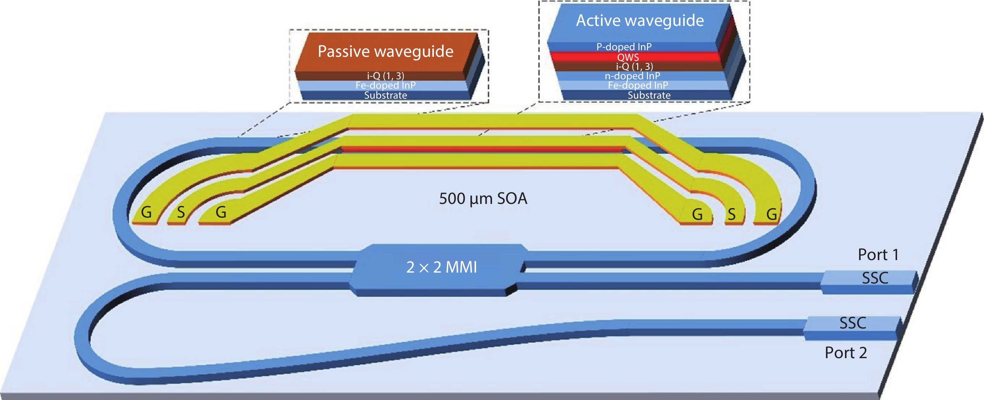
Fig. 1 shows the schematic diagram of the proposed microring modulator. The device is fabricated on the InP platform and mainly consists of a racetrack microring, which includes an SOA and is coupled to a bus waveguide through a MMI coupler. The incorporated SOA is 500 μm long and designed to supply 10 dB gain at most. Maximum 20 GHz traveling wave electrodes are employed to SOA to realize the modulation, which are from the standard process design kite (PDK, supplied by HHI, Gemany). To achieve the maximum modulation speed, bias ports of the electrodes could be used bidirectionally, in which one of them should be terminated with a 50 Ω impedance. A 2 × 2 MMI coupler is used to connect the racetrack microring and the bus waveguide due to the good fabrication tolerance of the MMI coupler. Two spot size converters (SSCs) are adopted at the two ports of the bus waveguide, respectively. Distance between the two SSCs is 250 μm, according with the separation of the standard single-mode fiber array, which is convenient for butt-coupling test and package.
![]()
Figure 1.(Color online) Architecture of the microring modulator.
The bending radius of the racetrack microring is 300 μm and the perimeter is 4.14
An optical microscope image of the device with a scale bar of 200 μm is shown in Fig. 2(a), in which the SSCs are outside the view because of the minimum magnification times limitation. The way to couple the optical and electrical signal is illustrated in Fig. 2(b) that a two ports standard single-mode fiber array (FA) is coupled to the two ports of the microring modulator through SSCs. Probe 1 carries the electrical signal to one port of the traveling wave electrode on the chip, while probe 2 connects a 50 Ω impedance to the other port of the electrode. There is a copper block under the chip for heat dissipation.
![]()
Figure 2.(Color online) (a) A photograph of the microring modulator with a scale bar of 200
3. Characterization and experimental results
To characterize the modulator, the I–V curve of the SOA is measured when the 50 Ω impedance is disconnected because the SOA is usually driven by injection currents. And the I–V curve could relate currents with the corresponding voltage. A source-measure unit (SMU) and a bias tee are applied to test the I–V curve which is plotted and fitted in Fig. 3. Only a maximum 190 mA current is applied, avoiding the damage of the SOA.
![]()
Figure 3.The
Then a high-resolution optical vector network analyzer (OVNA) is established to measure the static transmission and phase spectra of the designed microring modulator. An optical carrier generated by the laser (Yenista, Tunics T1005-HP) and modulated by radio frequency (RF) signal from the electrical vector network analyzer (ZVA 40) through the phase modulator (EOSPACE, 40G). And an optical double-sideband (ODSB) signal is produced and one sideband is filtered out by the tunable filter to generate an optical single-sideband (OSSB). The OSSB signal is amplified by an erbium-doped fiber amplifier (EDFA) and coupled to the chip via the input port SSC. After the transmission through the device, the OSSB signal is injected to one photodetector (FINISAR XPDV2120R) to beat and generate RF signal. The RF signal is fed back to the electrical vector network analyzer (EVNA) after the amplification of an electrical amplifier (EA). The S21 curve exhibits the transmission spectra of the device and the resolution is decided by the EVNA, which could achieve tens of Hz resolution. The characterization of the device could be more precisely measured by this OVNA[
The transmission spectra of the modulator at four different injection currents are displayed in Fig. 4(a). There are four lines representing the transmission spectra of the device for 136.74, 137.24, 137.74, and 138.24 mA injection currents. When the current of SOA is set to 138.24 mA, the microring resonator operates around the ideal critical coupling point, in which the ER is over 43 dB. As improving the injection current, the gain of SOA could compensate for the loss in the microring. The current is delicately tuned to adjust the relation between the loss coefficient and coupling coefficient, while the transmission spectra could be observed in real time through OVNA. Once the coupling coefficient between the bus waveguide and the microring equals the loss coefficient in the microring, the active microring resonator will be under critical coupling condition, wherein the ER is theoretically infinite at the resonance wavelength. To estimate the coupling state of the microring resonator, the phase data recorded by the EVNA is processed with the formula:
![]()
Figure 4.(Color online) (a) The transmission spectra of the microring modulator under four injection currents applied to the SOA. (b) Modulation depth and insertion loss with currents from 136.74 to 138.24 mA.
To measure the modulation bandwidth, a 50 Ω impedance is applied to the chip to reduce the reflection of the microwave signal. The experiment link is shown in Fig. 5. A 1550.005 nm carrier wave is coupled to the modulator to enable the microring modulator operate at the linear operating point. And a 186.6 mA bias current is applied, in which a 137.5 mA will be set to SOA according to the I–V curve in Fig. 3(a) and the tested static transmission spectra in Fig. 4(a). Using the EVNA to measure the S21 of this modulator from 0 to 20 GHz with the power of 9 dBm, which is presented in Fig. 6. The 3 dB bandwidth of the microring modulator is about 6.6 GHz. Because the traveling electrodes are from the standard PDK, the bandwidth is mainly limited by the QCSE. What is more, optimizing the electrode and waveguide design, improving the growth of InP quantum wells, and reducing the radius of the microring could improve the 3 dB bandwidth of the microring modulator.
![]()
Figure 5.(Color online) The experiment schematic of the modulation bandwidth measurement.
![]()
Figure 6.The bandwidth of the device when it works as an electro–optic modulator.
Applied in the back-to-back configuration, eye diagrams are measured. Figs. 7(a)–7(c) show measured eye diagrams under the transmission of 4, 8, and 12 Gb/s PRBS 27–1 NRZ data signals, respectively. As can be seen in Fig. 7, the eye could open clear when the modulating signal reaches 8 Gb/s. Nevertheless, when the data speed exceeds 10 Gb/s, the eye diagrams are hard to open because of the noise and the nonlinearity in the test link. The proposed microring modulator may be employed in the optical communication link. To improve the modulation speed, the fabrication process and electrodes design could be modified.
![]()
Figure 7.(Color online) Measured eye diagrams of the device under 4, 8, and 12 Gb/s bit rates.
4. Conclusion
In conclusion, an ultra-low Vpp and high-modulation-depth InP-based electro–optic microring modulator is designed, fabricated, and characterized. The Vpp reaches as low as 11 mV and the modulation depth is 42.5 dB in maximum. The microring modulator shows a 6.6 GHz bandwidth and measured eye diagrams up to 12 Gb/s bit rate demonstrate the ability of the proposed device in the optical communication link. The realization of the microring modulator broadens the applications and promotes the designability of the basic building blocks in PIC.
Acknowledgements
This work was supported by the National Natural Science Foundation of China (61535012, 61925505) and the National Key R&D Program of China (2018YFB2201900). The authors acknowledge VLC, Spain, for their help in designing this chip. The authors acknowledge HHI, Germany, for the chip fabrication.
References
[1] R Soref. The past, present, and future of silicon photonics. IEEE J Sel Top Quantum Electron, 12, 1678(2006).
[2] L Thylén, L Wosinski. Integrated photonics in the 21st century. Photon Res, 2, 75(2014).
[3] J Zhang, M A Itzler, H Zbinden et al. Advances in InGaAs/InP single-photon detector systems for quantum communication. Light: Sci Appl, 4, e286(2015).
[4] Z C Wang, B Tian, M Pantouvaki et al. Room-temperature InP distributed feedback laser array directly grown on silicon. Nat Photonics, 9, 837(2015).
[5] J Müller, F Merget, Azadeh S Sharif et al. Optical peaking enhancement in high-speed ring modulators. Sci Rep, 4, 6310(2014).
[6] H T Lin. Mid-infrared lasers on silicon operating close to room temperature. J Semicond, 40, 100202(2019).
[7] X L Cai. Progress in integrating III–V semiconductors on silicon could drive silicon photonics forward. J Semicond, 40, 100301(2019).
[8] C Zhao, B Xu, Z J Wang et al. Boron-doped III–V semiconductors for Si-based optoelectronic devices. J Semicond, 41, 011301(2020).
[9] C H Li, J Deng, W Y Sun et al. Improvement of tunnel compensated quantum well infrared detector. J Semicond, 40, 122902(2019).
[10]
[11]
[12] J Hofrichter, O Raz, A La Porta et al. A low-power high-speed InP microdisk modulator heterogeneously integrated on a SOI waveguide. Opt Express, 20, 9363(2012).
[13] T Sadagopan, S J Choi, S J Choi et al. Carrier-induced refractive index changes in InP-based circular microresonators for low-voltage high-speed modulation. IEEE Photonics Technol Lett, 17, 414(2005).
[14] S Andreou, A Millan-Mejia, M Smit et al. Slot waveguide microring modulator on InP membrane. 20th Annual Symposium of the IEEE Photonics Benelux Chapter, 23(2015).
[15] Q Xu, B Schmidt, S Pradhan et al. Micrometre-scale silicon electro-optic modulator. Nature, 435, 325(2005).
[16] S Manipatruni, K Preston, L Chen et al. Ultra-low voltage, ultra-small mode volume silicon microring modulator. Opt Express, 18, 18235(2010).
[17] K Padmaraju, J Chan, L Chen et al. Thermal stabilization of a microring modulator using feedback control. Opt Express, 20, 27999(2012).
[18] M S Hai, M M P Fard, O Liboiron-Ladouceur. A low-voltage PAM-4 SOI ring-based modulator. 2014 IEEE Photonics Conference, 194(2014).
[19] M Gould, T Baehr-Jones, R Ding et al. Silicon-polymer hybrid slot waveguide ring-resonator modulator. Opt Express, 19, 3952(2011).
[20] P Dong, S Liao, D Feng et al. Low Vpp, ultralow-energy, compact, high-speed silicon electro-optic modulator. Opt Express, 17, 22484(2009).
[21] P Dong, R Shafiiha, S Liao et al. Wavelength-tunable silicon microring modulator. Opt Express, 18, 10941(2010).
[22] L Chen, Q Xu, M G Wood et al. Hybrid silicon and lithium niobate electro-optical ring modulator. Optica, 1, 112(2014).
[23] Y Hu, X Xiao, H Xu et al. High-speed silicon modulator based on cascaded microring resonators. Opt Express, 20, 15079(2012).
[24] Z Tang, S Pan, J Yao. A high resolution optical vector network analyzer based on a wideband and wavelength-tunable optical single-sideband modulator. Opt Express, 20, 6555(2012).
[25] T Baba, S Akiyama, M Imai et al. 50-Gb/s ring-resonator-based silicon modulator. Opt Express, 21, 11869(2013).
[26] X Xiao, H Xu, X Li et al. 25 Gbit/s silicon microring modulator based on misalignment-tolerant interleaved PN junctions. Opt Express, 20, 2507(2012).
[27] Q F Xu, S Manipatruni, B Schmidt et al. 12.5 Gbit/s carrier-injection-based silicon micro-ring silicon modulators. Opt Express, 15, 430(2007).
[28] F N Xia, L Sekaric, Y Vlasov. Ultracompact optical buffers on a silicon chip. Nat Photonics, 1, 65(2007).
[29] Q F Xu, D Fattal, R G Beausoleil. Silicon microring resonators with 1.5-µm radius. Opt Express, 16, 4309(2008).
[30] Y Okawachi, K Saha, J S Levy et al. Octave-spanning frequency comb generation in a silicon nitride chip. Opt Lett, 36, 3398(2011).
[31] H C Frankis, K M Kiani, D Su et al. High-
[32] M Zhang, C Wang, R Cheng et al. Monolithic ultra-high-Q lithium niobate microring resonator. Optica, 4, 1536(2017).
[33] A Guarino, G Poberaj, D Rezzonico et al. Electro–optically tunable microring resonators in lithium niobate. Nat Photonics, 1, 407(2007).
[34] M Zhang, B Buscaino, C Wang et al. Broadband electro-optic frequency comb generation in a lithium niobate microring resonator. Nature, 568, 373(2019).
[35] X F Fang, L Yang. Thermal effect analysis of silicon microring optical switch for on-chip interconnect. J Semicond, 38, 104004(2017).
[36] V M Menon, W Tong, S R Forrest. Control of quality factor and critical coupling in microring resonators through integration of a semiconductor optical amplifier. IEEE Photonics Technol Lett, 16, 1343(2004).
[37] B E Little, S T Chu, H A Haus et al. Microring resonator channel dropping filters. J Lightwave Technol, 15, 998(1997).
[38] D G Rabus, Z X Bian, A Shakouri. Ring resonator lasers using passive waveguides and integrated semiconductor optical amplifiers. IEEE J Sel Top Quantum Electron, 13, 1249(2007).
[39] K Amarnath, R Grover, S Kanakaraju et al. Electrically pumped InGaAsP-InP microring optical amplifiers and lasers with surface passivation. IEEE Photonics Technol Lett, 17, 2280(2005).
[40] M Fujii, C Koos, C Poulton et al. Nonlinear FDTD analysis and experimental verification of four-wave mixing in InGaAsP-InP racetrack microresonators. IEEE Photonics Technol Lett, 18, 361(2006).
[41] L X Zou, Y Z Huang, X M Lv et al. Modulation characteristics and microwave generation for AlGaInAs/InP microring lasers under four-wave mixing. Photon Res, 2, 177(2014).
[42] W Jun, L Wang, C Yang et al. Optical vector network analyzer based on double-sideband modulation. Opt Lett, 42, 4426(2017).

Set citation alerts for the article
Please enter your email address
© Copyright 2018-2021 | Chinese Laser Press. All Rights Reserved 沪ICP备15018463号-20