
Jie Zhang, Yong Zhu. Slot-Waveguide Coupled Nanostructure Enhanced Raman Spectroscopy[J]. Acta Optica Sinica, 2020, 40(3): 0313001
- Acta Optica Sinica
- Vol. 40, Issue 3, 0313001 (2020)
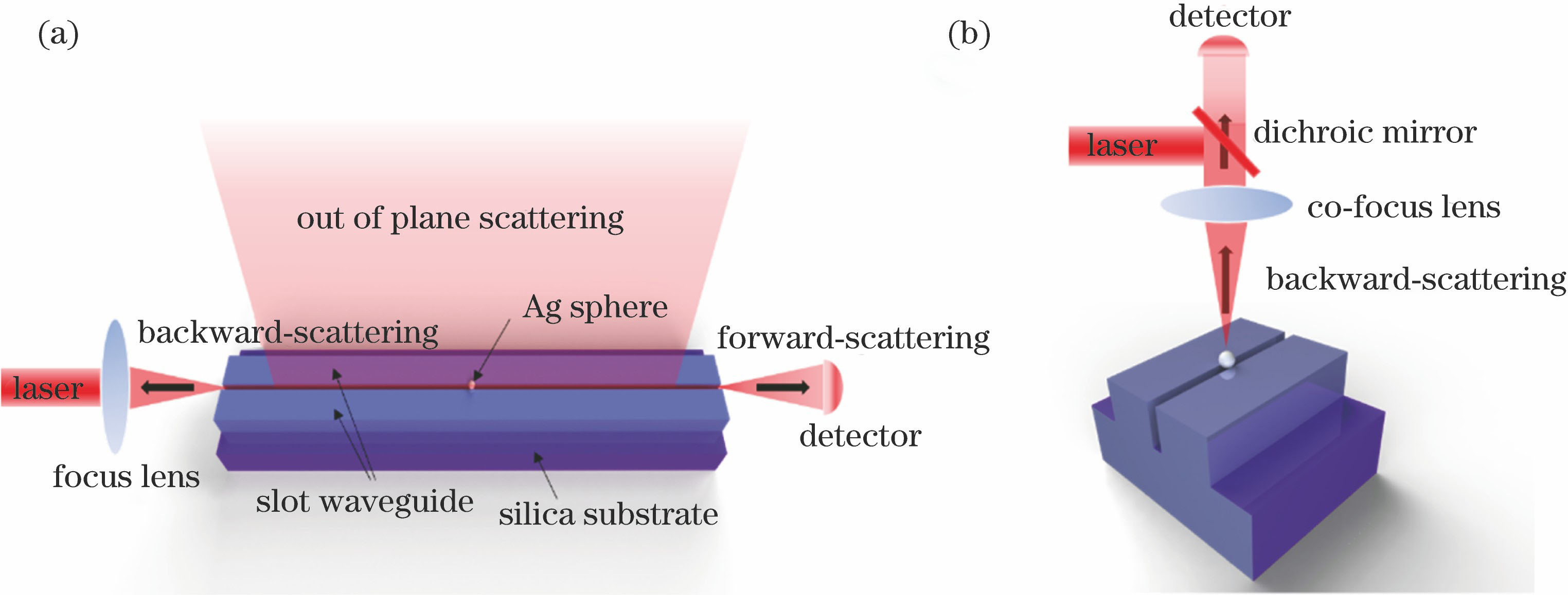
Fig. 1. Schematic of Raman scattering in different structures. (a) Slot-waveguide coupling structure; (b) free space
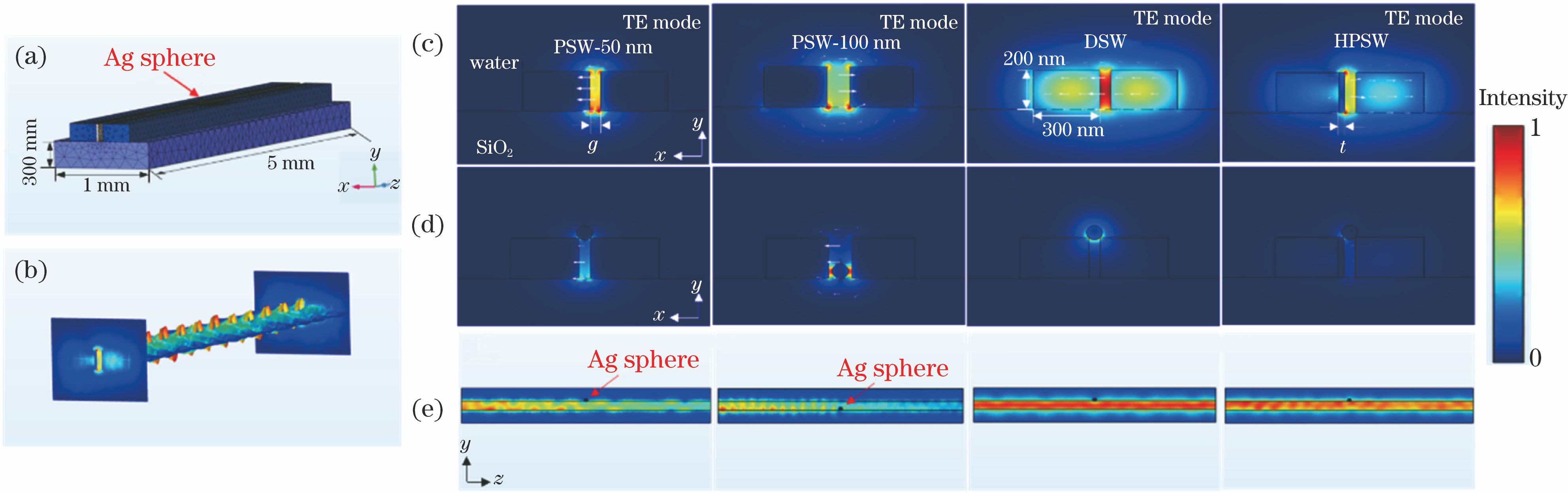
Fig. 2. Electric field distributions of slot waveguide. (a) Mesh division of the 3D model; (b) 3D model distribution; (c) normalized mode distributions of quasi-transverse electric (TE) modes of PSW with width of 50 nm, PSW with width of 100 nm, DSW, and HPSW respectively, and the arrow is polarization direction of electric field; (d) normalized electric field distributions of the corresponding waveguide coupling Ag nanosphere structure on the XY plane at center of the nanosphere; (e) normalized
Fig. 3. Propagation characteristics of different waveguides. (a) Relationship between the Possel factor and the wavelength; (b) waveguide collection percentage as a function of wavelength
Fig. 4. Electric field distributions in free space. (a) Mesh division of COMSOL model; (b)~(e) normalized electric field distributions on XY plane corresponding to Fig. 2 (d)
Fig. 5. Raman enhancement factors of different waveguides as functions of propagation distance. (a) FESM as a function of longitudinal propagation distance Z; (b) FEA as a function of longitudinal propagation distance Z. The solid lines represent FEA of backscattering and dashed lines represent FEA of out-of-plane scattering

Set citation alerts for the article
Please enter your email address
© Copyright 2018-2021 | Chinese Laser Press. All Rights Reserved 沪ICP备15018463号-20