• Advanced Photonics Nexus
  • Vol. 2, Issue 4, 046003 (2023)
Jiabin Yan*, Li Fang, Zhihang Sun, Hao Zhang, Jialei Yuan, Yan Jiang, and Yongjin Wang*
Author Affiliations
  • Nanjing University of Posts and Telecommunications, Peter Grünberg Research Center, Nanjing, China
  • show less
    DOI: 10.1117/1.APN.2.4.046003 Cite this Article Set citation alerts
    Jiabin Yan, Li Fang, Zhihang Sun, Hao Zhang, Jialei Yuan, Yan Jiang, Yongjin Wang. Complete active–passive photonic integration based on GaN-on-silicon platform[J]. Advanced Photonics Nexus, 2023, 2(4): 046003 Copy Citation Text show less
    Schematic diagram of the proposed photonic integrated chip.
    Fig. 1. Schematic diagram of the proposed photonic integrated chip.
    Images of the fabricated photonic integrated chip. (a) SEM image of the complete chip; (b) enlarged SEM image of the slot between the receiver and Y-branch waveguide; (c) SEM cross-sectional image of the modulator; (d) enlarged SEM image of the modulator edge; (e) enlarged SEM image of the top epilayers; and (f) cross-sectional scanning transmission electron microscope image of the top epilayers.
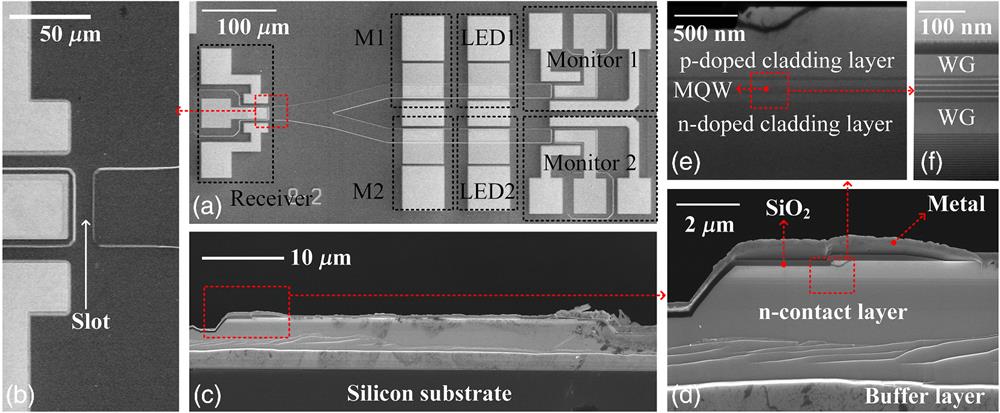
    Fig. 2. Images of the fabricated photonic integrated chip. (a) SEM image of the complete chip; (b) enlarged SEM image of the slot between the receiver and Y-branch waveguide; (c) SEM cross-sectional image of the modulator; (d) enlarged SEM image of the modulator edge; (e) enlarged SEM image of the top epilayers; and (f) cross-sectional scanning transmission electron microscope image of the top epilayers.
    (a) Leakage currents between the p-contact electrodes; (b) IV characteristics of MQW diodes and CV characteristics of the receiver; (c) PL spectra of the MQW diode; (d) RS and EL spectra of the MQW diode; (e) detected photocurrent of the receiver and monitor1 versus the injection currents on L1; (f) detected photocurrent of the receiver under different applied currents on L1.
    Fig. 3. (a) Leakage currents between the p-contact electrodes; (b) IV characteristics of MQW diodes and CV characteristics of the receiver; (c) PL spectra of the MQW diode; (d) RS and EL spectra of the MQW diode; (e) detected photocurrent of the receiver and monitor1 versus the injection currents on L1; (f) detected photocurrent of the receiver under different applied currents on L1.
    (a) Detected photocurrent versus the bias voltage on M1; (b) detected photocurrent of receiver and monitor1 when a square signal is applied on M1; (c) photocurrent waveform of the receiver under different injection currents on L1; (d) received waveform of the receiver when two modulation signals with different frequencies (20 and 200 Hz) are simultaneously applied on the modulators. Inset displays the PIC chip in the working state (Video 1, MPEG, 9.1 MB [URL: https://doi.org/10.1117/1.APN.2.4.046003.s1). (e) Detected photocurrent of the receiver at a modulation frequency of 1 Hz on M1 over 2000 circles. The injected current on L1 is 20 mA, and the modulation voltage ranges from −8 to −4 V.
    Fig. 4. (a) Detected photocurrent versus the bias voltage on M1; (b) detected photocurrent of receiver and monitor1 when a square signal is applied on M1; (c) photocurrent waveform of the receiver under different injection currents on L1; (d) received waveform of the receiver when two modulation signals with different frequencies (20 and 200 Hz) are simultaneously applied on the modulators. Inset displays the PIC chip in the working state (Video 1, MPEG, 9.1 MB [URL: https://doi.org/10.1117/1.APN.2.4.046003.s1). (e) Detected photocurrent of the receiver at a modulation frequency of 1 Hz on M1 over 2000 circles. The injected current on L1 is 20 mA, and the modulation voltage ranges from 8 to 4  V.
    Combined signals detected by the receiver with (a) an incident signals with varying duty cycles on M1; (b) the incident two signals in different phases. Eye diagram using (c) indirect modulation at a data transmission rate of 10 kbps and (d) direct modulation at a data transmission rate of 40 Mbps.
    Fig. 5. Combined signals detected by the receiver with (a) an incident signals with varying duty cycles on M1; (b) the incident two signals in different phases. Eye diagram using (c) indirect modulation at a data transmission rate of 10 kbps and (d) direct modulation at a data transmission rate of 40 Mbps.
    Jiabin Yan, Li Fang, Zhihang Sun, Hao Zhang, Jialei Yuan, Yan Jiang, Yongjin Wang. Complete active–passive photonic integration based on GaN-on-silicon platform[J]. Advanced Photonics Nexus, 2023, 2(4): 046003
    Download Citation