
Mengmeng Ma, Yanbin Huang, Jun Liu, Kong Liu, Zhijie Wang, Chao Zhao, Shengchun Qu, Zhanguo Wang. Engineering the photoelectrochemical behaviors of ZnO for efficient solar water splitting[J]. Journal of Semiconductors, 2020, 41(9): 091702
- Journal of Semiconductors
- Vol. 41, Issue 9, 091702 (2020)
![(Color online) PEC water splitting in (a) the n-type semiconductor-based PEC system, (b) p-type semiconductor-based PEC system, and (c) tandem system[6].](/richHtml/jos/2020/41/9/091702/img_1.jpg)
Fig. 1. (Color online) PEC water splitting in (a) the n-type semiconductor-based PEC system, (b) p-type semiconductor-based PEC system, and (c) tandem system[6 ].
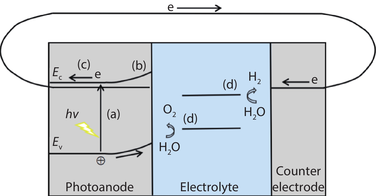
Fig. 2. (Color online) Main processes of PEC water splitting for n-type semiconductors.
Fig. 3. (Color online) (a) ZnO model of the hexagonal wurtzite structure, (b) schematic illustrations of atoms and charges distribution in the unit cell of Wurlitzer-structure ZnO, where F and P represent the applied stress and the induced electric dipole moment, respectively[11 ].
Fig. 4. (Color online) Energy potentials of ZnO and redox potentials for PEC water splitting at pH = 7, relative to NHE (normal hydrogen electrode).
Fig. 5. (Color online) Carrier transport mechanism of the ZnO photoanode.
Fig. 6. (Color online) Schematic illustration of the preparation processes of CS ZnO/TiO2 and BN ZnO/TiO2[24 ].
Fig. 7. (Color online) Effect of element doping on band structure[27 ].
Fig. 8. (Color online) (a) Schematic diagram of N gradient doped ZnO nanorods and stepped band structure to promote carrier separation[15 ]. (b) Morphological benefits of Y doping and schematic of increased electron mobility from trap filling[30 ].
Fig. 9. (Color online) Schematic diagrams of the forms of (a) type-II junction, (b) p–n junction, (c) Z-scheme system, and (d) hot-electron injection[3 ].
Fig. 10. (Color online) Schematic illustration of the proposed mechanism for the charge transfer (a) in ZnWO4/ZnO photoanode[31 ], (b) between ZnO and MoSx co-catalyst[32 ], (c) for the system of ZnO/CdS/PbS ONTs[19 ], and (d) ZnO–Au–SnO2[34 ].
Fig. 11. (Color online) (a) Bilateral CdS–ZnO–ZnO–CdSe nanowire array photoanode structure and corresponding energy level diagram[37 ]. (b) Synthetic route diagram and (c) schematic of the potential energy diagram of the ZnO/ZnFe2O4/PbS nanorod arrays electrode[38 ].
Fig. 12. (Color online) (a) The main mechanism of Au/3D ZnO nanowire photoelectrode[40 ]. (b) Schematic diagram of bending the sample to bending radius R under light[41 ].
Fig. 13. (Color online) Schematic band alignment of charge transport and recombination models in (a) ZnO and (b) FVO/ZnO photoanodes[48 ].
Fig. 14. (Color online) Piezo-phototronic effect on the photoelectrocatalytic process (photoanode). Illustration of the photoelectrocatalytic process (a) without strain, (b) under tensile strain, and (c) under compressive strain[11 ].
Fig. 15. (Color online) Schematic illustration of the enhanced catalytic performance induced by piezotronic effect and unique asymmetric nanostructure under light irradiation and ultrasonic actuation (ϕ SB, Schottky barrier; E CB and E VB, the CB and VB of ZnO, respectively; E f, the Fermi level of the Asy–Au–ZnO composite structure)[53 ].

Set citation alerts for the article
Please enter your email address
© Copyright 2018-2021 | Chinese Laser Press. All Rights Reserved 沪ICP备15018463号-20