• Journal of Semiconductors
  • Vol. 41, Issue 9, 091702 (2020)
Mengmeng Ma1、2, Yanbin Huang1、3, Jun Liu1、2, Kong Liu1、2, Zhijie Wang1、2, Chao Zhao1、2, Shengchun Qu1、2, and Zhanguo Wang1、2
Author Affiliations
  • 1Key Laboratory of Semiconductor Materials Science, Beijing Key Laboratory of Low Dimensional Semiconductor Materials and Devices, Institute of Semiconductors, Chinese Academy of Sciences, Beijing 100083, China
  • 2Center of Materials Science and Optoelectronics Engineering, University of Chinese Academy of Sciences, Beijing 100049, China
  • 3School of Mathematical Science and Engineering, Hebei University of Engineering, Handan 056038, China
  • show less
    DOI: 10.1088/1674-4926/41/9/091702 Cite this Article
    Mengmeng Ma, Yanbin Huang, Jun Liu, Kong Liu, Zhijie Wang, Chao Zhao, Shengchun Qu, Zhanguo Wang. Engineering the photoelectrochemical behaviors of ZnO for efficient solar water splitting[J]. Journal of Semiconductors, 2020, 41(9): 091702 Copy Citation Text show less

    Abstract

    Solar water splitting is a promising strategy for the sustainable production of renewable hydrogen and solving the world’s crisis of energy and environment. The third-generation direct bandgap semiconductor of zinc oxide (ZnO) with properties of environmental friendliness and high efficiency for various photocatalytic reactions, is a suitable material for photoanodes because of its appropriate band structure, fine surface structure, and high electron mobility. However, practical applications of ZnO are usually limited by its high recombination rate of photogenerated electron–hole pairs, lack of surface reaction force, inadequate visible light response, and intrinsic photocorrosion. Given the lack of review on ZnO’s application in photoelectrochemical (PEC) water splitting, this paper reviews ZnO’s research progress in PEC water splitting. It commences with the basic principle of PEC water splitting and the structure and properties of ZnO. Then, we explicitly describe the related strategies to solve the above problems of ZnO as a photoanode, including morphology control, doping modification, construction of heterostructure, and the piezo-photoelectric enhancement of ZnO. This review aims to comprehensively describe recent findings and developments of ZnO in PEC water splitting and to provide a useful reference for the further application and development of ZnO nanomaterials in highly efficient PEC water splitting.

    1. Introduction

    Under the demand of global sustainable development, solar energy and hydrogen energy are two clean and environmentally friendly new energy sources that attract full attention. With the help of photocatalysts, artificial simulation of photosynthesis in green plants can simultaneously achieve the absorption and utilization of sunlight and the production of hydrogen and oxygen by solar water splitting.

    In 1972, Fujishima et al. from Japan discovered that under the illumination of near-ultraviolet light (380 nm), the rutile TiO2 single crystal electrode could split water into H2 and O2 at normal temperature[1], providing the possibility of generating hydrogen directly by solar water splitting. Scientists called this technology of producing hydrogen and oxygen only by sunlight and water as “one of the ideal technologies for humans”. From the perspective of solar energy utilization, producing hydrogen by solar water splitting mainly uses the ultraviolet and visible part of solar radiation. At present, two technologies, including photoelectrocatalysis (PEC) and photocatalysis (PC), are applied to prepare hydrogen from solar water splitting. PC technology is used to disperse the photocatalyst in the form of fine powder in the electrolyte to form a particulate suspension system. Although the PC system is regarded as the lowest-cost system for solar water splitting, its practical application is hampered by the high recombination rate of photogenerated charge carriers, limited visible-light absorption range, and low solar energy conversion efficiency of the photocatalyst. Compared with light excitation, the electric field is a more efficient driving force to separate the photogenerated carriers for solar water splitting. In this way, the PEC system, which is a combination of light excitation and the externally applied voltage, is constructed, and the separation efficiency of the photogenerated carriers can be significantly improved[2]. Even if the participation of bias voltage can enhance the separation of photogenerated carriers, the PEC system still requires efficient semiconductor materials as photoelectrodes. Among multitudinous semiconductors, ZnO is highly accepted with its high electron mobility (typically 10–100 folds more elevated than that of TiO2[3]) and low cost[4].

    Considering the extensive application of ZnO in PEC water splitting and the lack of relevant reviews, this paper will systematically describe the research of ZnO as a photoanode for solar water splitting. Firstly, the basic principle of PEC water splitting and the essential properties of ZnO, as well as related applications, are indispensably introduced. Secondly, several methods for enhancing the absorption efficiency of visible light, improving the efficiency of electron and hole separation, and improving the effectiveness of the surface catalytic reaction of ZnO-based photoanodes are described in this review, respectively, including morphology regulation, element doping, construction of the heterogeneous structure, and ferroelectric enhancement. This review aims to summarize recent findings and developments of ZnO-based photoanodes and to provide some useful guidance for the design and preparation of high-efficiency ZnO-based photoanodes for solar water splitting.

    1.1. The fundamental of photoelectrochemical water splitting

    With a semiconductor material fixed on a conductive substrate and working as an electrode, photogenerated electrons or holes are forced to move towards the opposite electrodes under an applied bias voltage, and thus the photogenerated carriers are separated. It is called the PEC method. Compared with photocatalytic water splitting using a powder-photocatalyst, PEC water splitting can not only compensate the valence band (VB) or conduction band (CB) potentials and overpotential of the semiconductor but also promote the separation of electrons and holes. Attributed to the existence of applied bias, PEC water splitting is expected to solve the problems of the high probability of electron–hole pair recombination, low apparent quantum yield, and low solar energy conversion efficiency of photocatalyst[2]. Besides, the PEC system has lower requirements on the CB and VB position of semiconductor materials, which means higher material selectivity. The PEC water splitting system has a simple mechanism and an environmentally friendly process. It can be perfectly combined with the existing photovoltaic technology, which is conducive to further industrial development[5]. The preparation of photoelectrode with low cost, stable and high photoelectric conversion efficiency is the key to this technique, which is generally composed of a photocatalyst formed on a glass substrate such as electrically conductive fluorine-doped tin oxide (FTO).

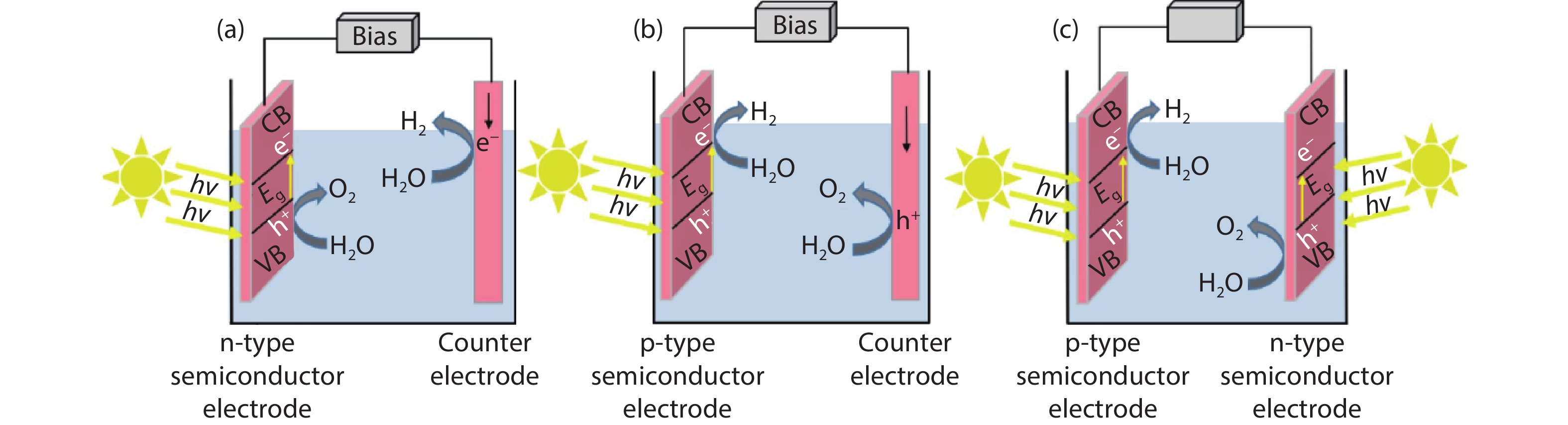
    In general, as depicted in Fig. 1, there are three types of PEC water splitting system: (a) the PEC system with n-type semiconductor materials as the photoanode and hydrogen evolution at the counter electrode; (b) the PEC system with a p-type semiconductor as the photocathode and oxygen evolution at the counter electrode; (c) the PEC system with n-type and p-type semiconductor as the photoanode and photocathode respectively, and hydrogen and oxygen evolution simultaneously.

    (Color online) PEC water splitting in (a) the n-type semiconductor-based PEC system, (b) p-type semiconductor-based PEC system, and (c) tandem system[6].

    Figure 1.(Color online) PEC water splitting in (a) the n-type semiconductor-based PEC system, (b) p-type semiconductor-based PEC system, and (c) tandem system[6].

    For a photoelectrochemistry device with an n-type semiconductor worked as the photoanode and hydrogen evolution at the counter electrode, the whole process at the photoanode can be divided into the following four steps (Fig. 2): (a) the absorption of light by the photoanode and the generation of photogenerated carriers; (b) the separation of carriers within the photoanode and at the solid–liquid interface; (c) carriers transport inside the photoanode; and (d) surface chemical redox reactions at the solid–liquid interface. In each of the above steps, there are energy losses, such as recombination and the capture of charge carriers, slow kinetics due to overpotential, and interruption of carrier transport. Therefore, the key to improving the conversion efficiency of PEC cells is to improve the photoanode performance of materials and minimize unnecessary energy losses.

    (Color online) Main processes of PEC water splitting for n-type semiconductors.

    Figure 2.(Color online) Main processes of PEC water splitting for n-type semiconductors.

    The selection of photoanode semiconductor nanomaterials for PEC cells is the top priority in the construction of an efficient PEC system. Four core problems corresponding to the above four steps must be considered: (1) the light absorption capacity of the photoanode and the generation efficiency of photogenerated carriers; (2) separation and transport efficiency of photogenerated electron–hole pairs; (3) carriers extraction at the photoanode/electrolyte interface and generation of electrochemical products; (4) stability of the photoanode in the electrolyte solution. Only by taking the above four factors into full consideration can a photoanode with high photoelectric conversion efficiency be obtained, so as to further improve the performance of the PEC water splitting system.

    1.2. Characteristics and related applications of ZnO

    Among copious semiconductor materials, the third-generation semiconductor ZnO nanomaterials are one of the most importantly exploited objects. ZnO is an n-type direct wide bandgap (Eg = 3.37 eV)[7] and a II–VI group metal oxide semiconductor. The large bandgap endows ZnO with high breakdown voltage, strong ability to maintain the electric field, low electronic noise, and high tolerable power. The bottom of ZnO’s CB is formed by the 4s state of Zn2+ ion or the anti-bond state of sp3 hybrid orbital, and the top of its VB is formed by the occupied state of O2– 2p orbital or the bound orbital of sp3 hybrid orbital[8]. ZnO has a high exciton binding energy up to 60 meV, which is much higher than that of other large bandgap semiconductor materials such as ZnSe (22 meV) and GaN (25 meV), so it can be applied at room temperature[9] or even higher temperatures. ZnO is widely used in the fields of optics, electricity, photoelectronic, sensing, energy, and catalysis due to its unique photoelectric, piezoelectric, thermoelectric properties, electric transport, field emission, dilute magnetism and wave absorption. ZnO nanomaterials are environmentally friendly, abundant, and easy to prepare. Also, among the obtained nanomaterials, ZnO has relatively high biosecurity and biocompatibility and is an excellent bio-adaptive semiconductor.

    Generally, there are three types of crystal phases for ZnO, including the hexagonal wurtzite structure, zinc blende, and rare rock salt structure. Among them, the wurtzite structure with the highest stability[10] under ambient conditions is the most common crystal type, with the coordination number of 4 : 4, the point group of 6 mm, and the spatial group of P63mc. As shown in Fig. 3(a), the lattice constants of wurtzite structure ZnO are as follows: a = 3.2496 Å and c = 5.2065 Å, and the measured lattice constants are as follows: a = 3.24–3.26 Å and c = 5.13–5.43 Å. The c/a ratio is about 1.60, which is close to the ideal hexagon ratio of 1.633. The structure of ZnO can be described as follows: the dense hexagonal accumulation of oxygen and zinc are nested in a reverse direction, that is, the O2– and Zn2+ planes in numerous layers are superimposed alternately along the direction of the c-axis, while the O2– or Zn2+ in two adjacent layers form a tetrahedral structure[7]. This bonding state and geometry lead to a non-central symmetry and a sizeable anisotropic property of ZnO, which exhibits intense spontaneous polarization (0.047 c/m2) and high electron mobility (at 300 K, ca.400 cm2V–1s–1) along the (0001) crystal plane, resulting in piezoelectric and thermoelectric effects along its c-axis. The centers of positive Zn2+ cations and negative O2– anions shift reversely when external strain is applied, leading to a dipole polarization (ionic charges) together with a built-in electric field (Fig. 3(b)). At present, the research of ZnO nanomaterials mainly focuses on, based on the controllable preparation of ZnO nanomaterials with high yield and the regulation of structure and performance, the realization of the assembly of prototype functional devices, the testing and evaluation of device performance, and the theoretical calculation and simulation work. Among the characteristics listed above, ZnO’s suitable band structure, earth-abundance of elements, high electron mobility, and the piezoelectric effect caused by lattice structure also contributes a lot to its application in PEC water splitting.

    (Color online) (a) ZnO model of the hexagonal wurtzite structure, (b) schematic illustrations of atoms and charges distribution in the unit cell of Wurlitzer-structure ZnO, where F and P represent the applied stress and the induced electric dipole moment, respectively[11].

    Figure 3.(Color online) (a) ZnO model of the hexagonal wurtzite structure, (b) schematic illustrations of atoms and charges distribution in the unit cell of Wurlitzer-structure ZnO, where F and P represent the applied stress and the induced electric dipole moment, respectively[11].

    2. Application of ZnO in PEC water splitting

    In the past few decades, many metal oxide semiconductor materials, including TiO2, ZnO, α-Fe2O3, BiVO4, WO3, and perovskite materials, have been widely studied and employed as photoanodes in PEC water splitting due to their excellent optical-electrical characteristic, suitable band structure (the VB position should be more positive than the redox potential of O2/H2O to ensure the oxidation characteristics of photogenerated holes, which is more conducive to the oxygen evolution reaction), the appropriate onset potential, high catalytic activity, and low cost in the process of the water oxidation reaction[12, 13]. In addition to these advantages, ZnO is widely applied for PEC water splitting due to its comparable efficiency to TiO2 in many catalytic reactions.

    As shown in Fig. 4, the bottom of the CB for ZnO is slightly more negative than the reduction potential of hydrogen, while the top of VB is far more positive than that of water oxidation. Thus, as a photoanode, ZnO has excellent advantages in conducting holes to water, which can enhance the separation of photogenerated electron–hole pairs at the photoanode and promote the PEC conversion efficiency of the whole system effectively.

    (Color online) Energy potentials of ZnO and redox potentials for PEC water splitting at pH = 7, relative to NHE (normal hydrogen electrode).

    Figure 4.(Color online) Energy potentials of ZnO and redox potentials for PEC water splitting at pH = 7, relative to NHE (normal hydrogen electrode).

    The advantages of ZnO nanomaterials in PEC water splitting are as follows: (1) ZnO nanomaterials usually have low reflectivity and strong light capture ability due to the fine nanostructure on the surface, which can endow ZnO with a high light absorption performance; (2) the surface of ZnO usually adsorbs abundant O2 molecules due to the existence of a large number of surface states. It then tends to capture photogenerated holes, which ultimately prolongs the lifetime of photogenerated electrons and improves the separation efficiency of photogenerated electron-hole pairs; (3) ZnO single crystal nanostructures with excellent crystallization performance prepared by various methods have high electron mobility[14] so that the carrier transport efficiency can be guaranteed; (4) the fine surface structure size of ZnO nanomaterials matches the diffusion length of minority carriers, thus improving the ability of charge extraction and ultimately enhancing the collection of carriers; (5) the band structure of ZnO endows the photogenerated holes with a strong oxidation ability. Therefore, ZnO is suitable for the photoanode material.

    However, ZnO has a wide bandgap and a band absorption edge at about 368 nm. It can only utilize the ultraviolet light, which accounts for only 4% of the solar spectrum[15]. There are also other problems with ZnO nanomaterials as photoanodes, as shown in Fig. 5: (i) the fast recombination of photogenerated carriers in the photoanode[16]; (ii) the fast recombination of electrons and holes at the interface between the photoanode and the electrolyte solution; and (iii) insufficient surface reactivity. Given the above problems, there are several effective strategies to improve the photoelectrocatalytic activity of ZnO, including expanding the absorption spectrum to the visible light region, enhancing the separation efficiency of photogenerated electron–hole pairs, and improving the surface reaction rate. These strategies are mainly implemented from the electrode/electrolyte interface or the inside of the electrode. For the electrode/electrolyte interface, there are usually four approaches: (1) constructing a hierarchical structure; (2) applying co-catalysts at the electrode/electrolyte interface; and (3) coating the passivation layer on the electrode at the electrode/electrolyte interface. For the inside of the electrode, it is mainly solved by element doping modification and constructing a heterojunction structure.

    (Color online) Carrier transport mechanism of the ZnO photoanode.

    Figure 5.(Color online) Carrier transport mechanism of the ZnO photoanode.

    2.1. The morphology control of ZnO

    At present, various morphologies of ZnO nanostructures can be prepared by a variety of deposition methods, physical and chemical synthesis methods, including nanoparticles of various shapes, nanowires, nanorods, and nanosheets, as well as relatively uncommon nanopencil and nanotetrapod structures.

    In the photocatalytic reaction, the low dimension catalytic nanomaterials have short photogenerated carrier migration paths, fast carriers migration efficiency, and a large surface area[17], resulting in excellent catalytic performance. Among almost all nanostructures, one-dimensional nanomaterials are the most suitable structural units for constructing nanoelectronics devices[18]. When the photoanode is a porous membrane composed of nanoparticles, the disordered accumulation of zero-dimensional structure makes the porous membrane have a large number of grain boundaries, and the photogenerated holes are easy to recombine at the grain boundaries during the irregular transmission process, which restricts the further improvement of photocatalytic performance to some extent. For arrays of the single-crystal structure perpendicular to the conductive base (such as nanotubes, nanorods, nanowires, nanotubes), a few photogenerated holes produced in the photoanode can quickly spread to the surface of the nanowire radially and react with the adsorbed water molecules to produce oxygen. Meanwhile, the corresponding photogenerated electrons can be transferred rapidly through the one-dimensional axial channel under the external voltage to produce hydrogen by the reduction reaction between the electrode and water.

    ZnO's one-dimensional nanostructure significantly improves its photoelectric and power transmission performance and is widely used in solar cells, PEC cells and other photoelectric conversion devices[19], or ultraviolet detection, biosensors, and other information sensors. Due to its high electron mobility, low onset potential, high intrinsic stability, and good environmental friendliness, one-dimensional ZnO is considered as a promising material for the preparation of a PEC photoanode. A ZnO nanorod array particularly has apparent advantages in the process of solar water splitting: its fewer grain boundaries provide a fast channel for electron transport; the scattering of incident light between the nanorods can improve the light absorption of the material; besides, the nanorod array grows directly on the substrate, which is beneficial to the recovery and reuse of photocatalyst.

    Zhang et al.[20] applied three different deposition methods, which are normal pulsed laser deposition (PLD), pulsed laser oblique-angle deposition (OAD), and electron-beam glancing-angle deposition (GLAD), to prepare nanostructure ZnO films. It showed that the grain size of the dense film prepared by normal PLD was 200 nm. Fish scale-shaped nanosheets were prepared by OAD with the particle size of 450–900 nm, while the crosslinked films with high porosity and particle size of 15–40 nm were produced by GLAD. For the above three deposition methods, the solar-to-hydrogen (STH) efficiency was 0.1%, 0.2%, and 0.6%, respectively. The corresponding results showed that the three kinds of thin films’ PEC properties depended on the porosity, crystal defect concentration, carrier transport, and space charge layer. In this work, the brown ZnO films prepared by the PLD method had a more extensive optical response range than those prepared by OAD and GLAD, which was caused by two defects of oxygen vacancy (VO) and Zn interstitial atoms (Zni). ZnO GLAD nanoparticle PEC cells generated the highest IpH (initial photocurrent) because of the improved charge transport, decreased defect density, and enhanced electron–hole separation caused by an increased semiconductor–electrolyte interaction. In comparison to PLD/OAD PEC cells, GLAD charge transport via diffusion from nanoparticle to nanoparticle was superior.

    Li et al.[21] first prepared ZnO nanowires by the hydrothermal method, then calcined them in an ammonia atmosphere, and introduced the N element to prepare the N-doped ZnO nanowire array photoanode. The N doping concentration was controlled by mediating the calcination time. IPCE (incident-photon-to-current-efficiency) test showed that compared with undoped ZnO nanowires, ZnO:N nanowires array had significantly enhanced optical response in the visible region, and its solar-to-hydrogen efficiency was 0.15% at 0.5 V vs. Ag/AgCl. By reducing the nanowires’ diameter to increase the active surface area, optimize the width of the depletion layer, and minimize the resistance between the nanowires and ITO (indium tin oxide) substrate, the PEC water splitting efficiency was improved.

    Yang et al.[22] synthesized secondary branching and the N-doped ZnO nanotetrapod for the study of PEC water splitting. It had good vectorial electron transmission characteristics and cross-networking characteristics. The photocurrent of the N-doped ZnO nanotetrapod was up to 0.99 mA/cm2 (0.31 V vs. Ag/AgCl). On the one hand, the improvement of photocurrent was due to the increased roughness of the ZnO nanotetrapod, which could enhance the light capture capability of ZnO dramatically; on the other hand, the doping of N element could reduce the bandgap of ZnO and enhance the visible light absorption capability of ZnO.

    Gong et al.[23] synthesized a ZnO nanopencil array modified with Au nanoparticles for PEC water splitting study. ZnO nanopencil arrays were grown on FTO (F doped SnO2) by liquid-phase chemical growth technology and then were modified with Au nanoparticles by photoreduction technology. The photocurrent of Au–ZnO nanopencil arrays reached 1.5 mA/cm2 at 1 V vs. Ag/AgCl, which was much higher than that of ZnO nanorods. The improved PEC performance of Au–ZnO nanopencils was due to the prolonged lifetime of photogenerated electron–holes caused by the surface plasmon resonance (SPR) effect of Au nanoparticles and the more efficient light absorption of nanopencils than that of nanorods as well.

    Li et al. firstly fabricated open bird-nest (BN) structured ZnO/TiO2 and sealed core-shell (CS) structured ZnO/TiO2 (Fig. 6)[24]. The BN ZnO/TiO2 showed the photocurrent densities of 1.05 mA/cm2 at 0.6 V (vs. RHE) and 2.75 mA/cm2 at 1.23 V (vs. RHE), which were 1.98 and 1.38 times higher than that of CS ZnO/TiO2, respectively. Also, the BN ZnO/TiO2 retained 96.2% of the initial photocurrent after eight hours of continuous irradiation, which is much better than CS ZnO/TiO2 (73.5%). The high surface area in BN ZnO/TiO2 led to the higher performance of PEC water splitting, because the larger interface contacting areas with electrolyte efficiently enhanced light-harvesting by forming a light trap and promoted carriers kinetics processes significantly due to more direct pathways for fast separation and transfer of carriers.

    (Color online) Schematic illustration of the preparation processes of CS ZnO/TiO2 and BN ZnO/TiO2[24].

    Figure 6.(Color online) Schematic illustration of the preparation processes of CS ZnO/TiO2 and BN ZnO/TiO2[24].

    The purpose of controlling the morphology of ZnO nanomaterials is mainly to increase the contact area between the semiconductor materials of photoanode and electrolyte or to change the surface roughness of the photoanode, so as to expose more reaction sites and reduce the carrier migration distance. Control of morphology is a fundamental method in the study of the material system, and it is generally combined with other means to improve PEC water splitting efficiency.

    2.2. The element doping of ZnO

    Through physical or chemical methods, the extra ions are injected into the semiconductor materials, and this method is called element doping. Additional doping can increase the donor concentration based on a certain number of electron donors[25]; in addition, it can also change the original lattice-type or form a defect energy level, thus affecting the mobility of charge carriers in semiconductor, adjusting their band structure or distribution, and then changing the PEC performance of the semiconductor materials. The effect of element doping onband structure is shown in Fig. 7.

    (Color online) Effect of element doping on band structure[27].

    Figure 7.(Color online) Effect of element doping on band structure[27].

    In order to improve the electronic and optical properties, and to inhibit inherent photocorrosion defects of ZnO as much as possible, several impurity atoms can be permeated into the lattice of ZnO. Currently, the common doped elements include Fe, Al, Cu, Co, Cr, Ni, C, Cl, and N elements[26], as well as relatively uncommon yttrium (Y) and solid compound solution. When doped elements enter the ZnO lattice, point defects will be generated, original electron energy level structure and Fermi-level of ZnO will be affected, thus narrowing the bandgap width and increasing the visible light absorption and conductivity.

    Theoretically, N-doping to replace significant amounts of the lattice oxygen with nitrogen (N2p orbitals are energetically more negative than O2p orbital) is a strategy designed to shift the VB higher[28]. Tong et al. synthesized a C and N-doped ZnO nanorod array for PEC hydrogen evolution[29]. The enhanced photocurrent and stability of the CN/ZnO nanorods were due to the enhanced light capture capability, reduced surface defects, and increased electron donor density. Shen et al. synthesized N-doped ZnO nanorods by ion implantation for the study of PEC water splitting in visible light[15]. The N-doped gradient distribution was realized along the vertical direction of the ZnO nanorod. At 1.1 V vs. SCE (saturated calomel electrode), the photocurrent reached 160 μA/cm2 in visible light, which was two orders of magnitude higher than that of the pristine ZnO nanorod array. The N-doped gradient distribution extended the optical absorption edge of ZnO to the visible region and formed a stepped band structure, which could effectively drive photogenerated electrons and holes (Fig. 8(a)).

    (Color online) (a) Schematic diagram of N gradient doped ZnO nanorods and stepped band structure to promote carrier separation[15]. (b) Morphological benefits of Y doping and schematic of increased electron mobility from trap filling[30].

    Figure 8.(Color online) (a) Schematic diagram of N gradient doped ZnO nanorods and stepped band structure to promote carrier separation[15]. (b) Morphological benefits of Y doping and schematic of increased electron mobility from trap filling[30].

    Commandeur et al. first synthesized Y-doped ZnO vertically aligned nanorods using a unique rapid microwave-assisted method[30]. The 0.1% Y-doped ZnO samples showed a 47% enhancement of PCE with a photocurrent of 0.84 mA/cm2 at 1.23 V (vs. RHE) and a more favorable geometry with higher aspect ratio along with reduced crystallinity because of substitutional defects, YZn. They indicated that the Y acted as a shallow n-type donor, which could increase the donor density in the ZnO NRs, leading to increased conductivity and reduced bandgap due to new states at the edge of the CB. Y doping resulted in faster electron mobility compared with pristine ZnO because of the filling of trap states. Overall, Y addition altered the formation energies of VZn and VO and led to higher concentrations of VZn and less VO, further impacting mobility and increasing hole concentration (Fig. 8(b)).

    2.3. The heterostructure construction of ZnO

    The construction of heterostructure with rational band alignment seems to be a very effective method to improve the performance of photoanode semiconductors in PEC water splitting. In the existing research, the heterostructure of ZnO is mainly constructed by utilizing the carrier separation effect of type-II, Z-scheme heterojunction or p–n junction, the quantum dot sensitization, the surface plasmon resonance of noble nanometals, the passivation layer of the heterojunction and the modified OER co-catalyst for the application of PEC water splitting. These are described in the categories as below.

    2.3.1. Construction of the ZnO-based heterojunction structure

    When other semiconductor materials are compounded with ZnO nanomaterials, three possible kinds of heterojunction will be formed, including a type-II junction, p–n junction, and Z-scheme system junction. The electron transport of these three heterojunctions is shown in Figs. 9(a)9(c). The type-II heterojunction is defined as the staggered alignment of the energy bands at the interface[3]. In the type-II heterojunction, electrons flow into the semiconductor with a more positive electrochemical potential corresponding to the CB’s bottom. At the same time, holes are restricted in the semiconductor with a more negative potential corresponding to the VB’s top. For the heterojunction of the Z-scheme system, the electron transfer between two materials is the profile of Z due to the electron transfer arranged according to the redox potential height. The built-in potential with the direction from an n-type semiconductor to a p-type semiconductor is the salient feature of a p–n junction, and it makes the p–n junction an efficient way of separating electron–hole pairs. The heterojunction of type-II, Z-scheme system, and p–n junction can effectively reduce the recombination rate and accelerate the separation and migration rates of the photogenerated carriers, thus improving the efficiency of PEC water splitting.

    (Color online) Schematic diagrams of the forms of (a) type-II junction, (b) p–n junction, (c) Z-scheme system, and (d) hot-electron injection[3].

    Figure 9.(Color online) Schematic diagrams of the forms of (a) type-II junction, (b) p–n junction, (c) Z-scheme system, and (d) hot-electron injection[3].

    Wannapop and Somdee[31] synthesized the ZnWO4/ZnO heterostructure (the ZnWO4 was grown on the hexagonal ZnO NRs) by a two-step hydrothermal method using TiO2 seed layers, which was applied as the photoanode for the PEC water splitting cell (as shown in Fig. 10(a)). Among all samples, the 50ZnW/ZnO sample showed the best performance of the PEC water splitting than others due to its more exceptional charge transfer between the photoanode and electrolyte, which was signified by the smaller arc compared to ZnO NRs in the Nyquist plot. In comparison to the pure ZnO, the ZnWO4/ZnO required the lower bias voltage to generate H2 and O2 according to the applied bias photo-to-current efficiency (ABPE) analysis.

    (Color online) Schematic illustration of the proposed mechanism for the charge transfer (a) in ZnWO4/ZnO photoanode[31], (b) between ZnO and MoSx co-catalyst[32], (c) for the system of ZnO/CdS/PbS ONTs[19], and (d) ZnO–Au–SnO2[34].

    Figure 10.(Color online) Schematic illustration of the proposed mechanism for the charge transfer (a) in ZnWO4/ZnO photoanode[31], (b) between ZnO and MoSx co-catalyst[32], (c) for the system of ZnO/CdS/PbS ONTs[19], and (d) ZnO–Au–SnO2[34].

    Amorphous MoSx was decorated on the surface of vertically grown ZnO thin sheets via the electrodeposition technique in Sharma’s work[32]. The determined band alignment of ZnO and MoSx indicated the formation of the type-II heterostructure, which allowed facile charge carrier separation. The sensitization of MoSx on the ZnO surface resulted in enhanced photocurrent density and increased photoconversion efficiency. The photocurrent density and carrier density were three times and 7.4-times higher than that of bare ZnO, respectively, and photoconversion efficiency of 0.934% was gained in the MoSx adorned ZnO. Besides, ZnO@MoSx thin sheets showed excellent stability even up to 1000 s under the chopped illumination condition (Fig. 10(b)).

    The p–n heterojunction of CuO/ZnO in nanorod array photoanodes was reported[33], and it showed simultaneous enhancement in charge separation and light-harvesting. A significant negative shift of 150 mV in the onset potential and an approximately 4-fold enhancement in the photocurrent at 1.23 V (vs. RHE) compared with those of pristine ZnO NRs that were acquired in the application of CuO/ZnO heterojunction photoanode for PEC water splitting.

    Zhang et al.[19] designed and prepared a photoanode composed of optimized ZnO/CdS/PbS nanotube arrays (ZnO/CdS/PbS NTs) with a multi-heterojunction structure via a three-step process, i.e., hydrothermal treatment, chemical bath deposition and successive ionic layer adsorption reaction (SILAR). The photocurrent density and PEC hydrogen evolution efficiency of the top-opened ZnO/CdS/PbS NTs reached up to 14.2 mA/cm2 and 5.5 mL/(cm2·h) at 0.0 V vs. Ag/AgCl, respectively. It turned out that the high PEC performance was ascribed to the large surface area of the top-opened nanotube structure and the well-matched band energy edge of the multi-heterojunction (Fig. 10(c)). These two kinds of optimization led to efficient light absorption, rapid mass transport, and efficient electron highways to deliver electrons, and a decreased recombination rate of photogenerated carriers, respectively.

    Hsu et al. firstly synthesized the ZnO–Au–SnO2 Z-scheme system photoanode for PEC water splitting, and the sample was prepared by the deposition of a thin layer of SnO2 on ZnO nanorods modified with Au nanoparticles[34]. For ZnO–Au–SnO2 nanorods, the embedded Au mediated the interface charge transfer by facilitating electron transfer from the CB of SnO2 to the VB of ZnO (Fig. 10(d)). This directional charge transfer led to the accumulation of photogenerated electrons in ZnO and photogenerated holes in SnO2, so ZnO–Au–SnO2 had a high redox capacity. Compared with original ZnO, Au-modified ZnO, and type-II SnO2 coated ZnO nanorods, ZnO–Au–SnO2 system nanorods as the photoanode had higher PEC water splitting activity.

    As mentioned earlier, due to the Z-scheme heterostructure formed between ZnO and TiO2, the PEC performance of the open BN ZnO/TiO2 fabricated by Li et al.[24] was significantly increased, and the Z-scheme band alignment for ZnO/TiO2 heterojunction was beneficial for suppressing the recombination of photogenerated carriers.

    2.3.2. The construction of ZnO heterogeneous structure based on quantum dot sensitization

    By modifying the quantum dot semiconductor materials on the ZnO photoanode system and combining it with the light absorption performance of the quantum dot, it is expected to solve the problem that the absorption region of ZnO is concentrated in the ultraviolet region. The modified ZnO-based semiconductor composite system with various band gaps has a broader spectral response range, resulting to the improved light absorption efficiency of ZnO. Semiconductor materials CdS and CdSe are widely used as modified quantum dots due to their narrow bandgap of 2.42 and 0.52 eV, respectively, and the corresponding light absorption cut-off wavelengths are 513 and 2387 nm, respectively. In addition to narrow-band gap semiconductors, low-dimensional carbon materials can also be used as sensitizers to promote the light absorption of ZnO.

    Liu et al. prepared single-layer CdTe quantum dot sensitized ZnO nanowire array photoelectrodes and realized the sensitization of CdX quantum dots to ZnO nanowires under the non-sacrificial agent electrolyte for the first time. The maximum PCE of the system was up to 1.83%, which was 200% higher than that of the original ZnO nanowires[35]. Li et al. used graphene quantum dots (GQDs) as green sensitizers to modify ZnO nanowire arrays for PEC water splitting[36]. Compared with the pristine ZnO nanowire photoelectrode, the open-circuit voltage and short circuit current density were significantly improved.

    Li et al. prepared a co-sensitized ZnO nanowire array of double-sided CdS and CdSe quantum dots for PEC hydrogen evolution[37]. The double-sided design provided a structure similar to a simple series pool, with dense ZnO nanowires arrays growing on both ITO substrates, and sensitized by CdS and CdSe quantum dots respectively (Fig. 11(a)). The composite photoelectrode exhibited strong absorption in the whole visible region, with the absorption limit of the long-wave reaching 650 nm, and its IPCE value was up to 45% at 0 V vs. Ag/AgCl. Under 100 mW/cm2 white light irradiation, the photocurrent density reached 12 mA/cm2 under 0.4 V vs. Ag/AgCl. Compared with the single quantum dot sensitized structure, the enhancement of photocurrent and IPCE value of double quantum dot sensitized structure was due to the band matching of CdS and CdSe in the electrolyte. In this work, two different kinds of semiconductor quantum dots with specific bandgap were first prepared for the integration of the bilateral nanowire photoanode, and it was proved to be efficient in PEC hydrogen evolution.

    (Color online) (a) Bilateral CdS–ZnO–ZnO–CdSe nanowire array photoanode structure and corresponding energy level diagram[37]. (b) Synthetic route diagram and (c) schematic of the potential energy diagram of the ZnO/ZnFe2O4/PbS nanorod arrays electrode[38].

    Figure 11.(Color online) (a) Bilateral CdS–ZnO–ZnO–CdSe nanowire array photoanode structure and corresponding energy level diagram[37]. (b) Synthetic route diagram and (c) schematic of the potential energy diagram of the ZnO/ZnFe2O4/PbS nanorod arrays electrode[38].

    Tian et al.[38] initially prepared ZnO nanorod/ZnFe2O4 nanosheet core/shell nanoarray as a stable heterojunction photoelectrode with rational band alignment and component control. This heterojunction was proved to enhance the visible light absorption significantly, accelerate charge carriers transfer and separation, and inhibit photocorrosion, thus improving the performance of PEC water splitting. To further promote charge transport and enhance visible light absorption of the photoelectrode, PbS quantum dots were decorated on it (Fig. 11(b)). The optimized ZnO/ZnFe2O4/PbS photoanode showed a significantly enhanced photocurrent density and excellent PEC stability measured in 0.1 M Na2SO4 electrolyte using a standard three-electrode configuration. Its photoconversion efficiency was 1.34 and 3.54 times higher than that of ZnO/ZnFe2O4 and ZnO nanorod array photoanodes, respectively, and 87.4% of the initial photocurrent density was obtained after 2 h light irradiation. The IPCE of ZnO/ZnFe2O4/PbS reached 54.99% at 350 nm, which was higher than that of ZnO/ZnFe2O4 NRs (45.18%) and ZnO NRs (28.65%).

    Han et al. explored the application of a unique combination of metal–organic framework (MOF)-decorated ZnO 1D nanostructures as the host and nitrogen-doped carbon dots (N-CDs) as the guest species in PEC water splitting[39]. In this work, the superior photocurrent density was ascribed to the enhanced absorption efficiency in the visible region. Carbon dots shows excellent potential as photosensitizers; nevertheless, the non-homogeneous anchoring and weak bonding between carbonaceous materials and semiconductor materials limit overall efficiency. Hence, N doping and the introduction of MOF were applied to overcome the challenges associated with the fabrication of well-arrayed CDs with many other photocatalytic heterostructures.

    2.3.3. The construction of heterostructure of ZnO based on the surface plasmon resonance

    When the frequency of the light is the same as the frequency of the electrons themselves on the surface of the metal, the valence electrons of some nano-sized metal particles (mainly precious metals, e.g., Au, Ag and Pt) oscillate collectively. In other words, resonance happens when the electron oscillation and the oscillating electric field have the same frequency; at this point, the metal nanoparticles show the light absorption ability. This phenomenon is the surface plasmon resonance effect of precious metals. Based on this, when noble metal nanoparticles are loaded on the ZnO matrix composite surface, the excited energy transferred from the nanometals could improve the absorption and scattering efficiency of the adjacent semiconductors. The hot electron injection to the semiconductor (as shown in Fig. 9(d)) and the enhanced local electric field are responsible for the improvement of PEC performance[3].

    Kang et al. prepared a 3D branched ZnO nanowire array modified with nano Au for PEC water splitting. This composite electrode exhibits excellent PEC activity in both the ultraviolet and visible region. The enhancement of optical activity in the visible region was due to the surface plasmon resonance effect of Au nanoparticles. The metal/semiconductor interface was conducive to the extraction of hot electrons from nanometer Au, so the PEC efficiency was improved (Fig. 12(a))[40]. Sun et al. prepared Ag-modified ZnO nanorods in the flexible polyethylene terephthalate (PET) substrate for PEC water splitting[41]. Plasma absorption enhancement was mediated by controlling the Ag thickness to inhibit the surface recombination rate and enhance the migration rate of charge carriers. Photon capture and absorption were further enhanced by controlling the degree of curvature of the PET substrate (Fig. 12(b)). When the thickness of Ag film was 10 nm, and the bending radius of the substrate was 6.0 mm, the short-circuit current density (Jsc) reaches 0.616 mA/cm2 and the photoelectric conversion efficiency (PCE) reaches 0.81%, which were 7 times and 10 times higher than the pure ZnO nanorods grown on the PET substrate, respectively. Gold nanoparticles were decorated on ZnO/CdS nanotube arrays (NTAs) to get plasmon-enhanced PEC water splitting performance[42]. In this work, the highest photocurrent density of 21.53 mA/cm2 at 1.2 V vs. Ag/AgCl and 3.45% PCE were exhibited when the optimized ZnO/CdS/Au NTAs photoanode was applied. The hot electrons generated by Au NPs greatly enhanced the transportation of photogenerated electrons, thus allowing more electrons to participate in PEC water splitting.

    (Color online) (a) The main mechanism of Au/3D ZnO nanowire photoelectrode[40]. (b) Schematic diagram of bending the sample to bending radius R under light[41].

    Figure 12.(Color online) (a) The main mechanism of Au/3D ZnO nanowire photoelectrode[40]. (b) Schematic diagram of bending the sample to bending radius R under light[41].

    2.3.4. Construction of ZnO heterogeneous structure based on the passivation layer and co-catalyst

    The oxidation potential of ZnO lies above the oxidation potential of water[43]; this means that ZnO could be oxidated in preference to water during the catalytic reaction, especially in acidic solution, which is called photocorrosion phenomena. Besides, the excitation of ZnO by an electrical bias or irradiation with sunlight causes additional decomposition processes[44]. The reduced chemical stability of ZnO in the electrolyte, to a certain extent, limits its practical application in PEC water splitting. Coating the protective layer on the surface of ZnO could not only help to passivate the surface states, thereby prolonging the lifetime of the photogenerated holes, but also helps to suppress photocorrosion by avoiding a direct interface of ZnO and the electrolyte[45], and the energy level matching and stability problems should be considered when selecting the passivation layer. The co-catalyst for oxygen evolution on the surface of ZnO can also promote the rate and efficiency of the water oxidation reaction, thus inhibiting the photocorrosion of ZnO.

    Zhang et al. constructed an ultra-thin TiO2 shell structure to improve the photocatalytic activity and chemical stability of the nanowires photoanode. The coating TiO2 could passivate the surface capture state of ZnO effectively, and compared with pure ZnO nanowires, the composite electrode had a 25% PEC efficiency improvement[46]. Duan et al. synthesized a ZnO nucleus-layered double hydroxide (LDH) shell, and this composite electrode achieved effective electron–hole separation due to the unusual electrocatalytic activity of the ZnO nucleus and LDH shell[47].

    Bamboo shoot-shaped FeVO4 (FVO, a novel and seldom studied n-type indirect bandgap semiconductor) passivated ZnO heterojunction nanorods photoanode was prepared for solar water splitting only by the spin-coating and calcination method[48]. The optimal photoanode without loading any co-catalyst afforded 130 mV negative shift in onset potential and 2.4 times augment in photocurrent density. The good stability and effective performance compared to pristine ZnO were attributed to the establishment of the heterojunction. The FeVO4-passivated layer, which has excellent chemical stability and high selectivity, was proved to eliminate the surface trapping state, thus increasing the photovoltage and promoting the interface charge transfer kinetics. The proposed band alignment model to describe the charge transfer behavior of FVO/ZnO photoanodes during PEC water oxidation is shown in Fig. 13, where krec and kct represent photogenerated charge carrier recombination in the bulk and transfer at the electrode-electrolyte interface, respectively.

    (Color online) Schematic band alignment of charge transport and recombination models in (a) ZnO and (b) FVO/ZnO photoanodes[48].

    Figure 13.(Color online) Schematic band alignment of charge transport and recombination models in (a) ZnO and (b) FVO/ZnO photoanodes[48].

    Metal–organic framework (MOF)-based transparent surface passivation layer modified ZnO nanorod arrays with Ni(OH)2 nanosheets grafted on as the co-catalyst were introduced for PEC water splitting[49]. The optimized Ni(OH)2/ZIF-8/ZnO/NF photoanode exhibited a 2-times higher photocurrent density of 1.95 mA/cm2 and also a 2-times more massive incident photon to the current conversion efficiency of 40.05% (350 nm) at 1.23 V (vs. RHE) than that of ZnO/NF. The ZIF-8 overlayer decreased the surface defects and improved the hole utilization, while the Ni(OH)2 nanosheets worked as a water oxidation co-catalyst. This synergetic modification led to the prolongation of carrier lifetime, the enhancement of charge transfer, and the decrease of overpotential for water oxidation.

    2.4. The piezo-photoelectric enhancement of ZnO

    Wurtzite ZnO exhibits an inherent piezotronic effect and piezo-phototronic effect[50] with the internal coupling of piezoelectric, semiconducting, and photonic properties[51]. When subjected to an external mechanical force, ZnO will generate a piezotronic potential (piezopotential), which could modulate the migration and separation of internal charge carriers, and subsequently rearrange band level, finally enhancing photocatalytic performance[52].

    In order to further solve the limited light utilization and fast charge carrier recombination of ZnO, the piezoelectric effect of ZnO also plays a particular role in PEC water splitting, realizing the synergy of piezocatalysis and photoelectrocatalysis. Under light and mechanical stress, the piezoelectric ZnO can generate charge carriers directly[53], and the piezopotential of ZnO can reduce the Schottky barrier formed between ZnO and plasmonic metals. Specifically, the built-in electric field caused by mechanical stimulation-induced polarization can serve as a flexible autovalve to modulate the charge-transfer pathway in designed directions and facilitate carrier separation both in the bulk phase and at the surfaces of the semiconductors[54].

    Initially, the electrons in the conduction band of an n-type semiconductor in a loop current tend to drift toward the semiconductor side due to the bent banding upward in the interface between the semiconductor and electrolyte, and then transport to the counter electrode through the external circuit. At the same time, the holes in the valance band can move toward the electrolyte directly. When a tensile strain is applied, the side directly interfacing with the electrolyte will have a negative piezopotential, which can lead to an upward bending of the band edge, thus efficiently reducing the local resistance or threshold voltage for the surface oxidation reaction. In comparison, if a compressive strain is applied, a positive piezopotential will be generated, which will lower and flatten the band edges at the semiconductor/electrolyte interface, thus reducing the driving force of electron–hole separation and reducing the redox efficiency (Fig. 14)[11].

    (Color online) Piezo-phototronic effect on the photoelectrocatalytic process (photoanode). Illustration of the photoelectrocatalytic process (a) without strain, (b) under tensile strain, and (c) under compressive strain[11].

    Figure 14.(Color online) Piezo-phototronic effect on the photoelectrocatalytic process (photoanode). Illustration of the photoelectrocatalytic process (a) without strain, (b) under tensile strain, and (c) under compressive strain[11].

    In order to generate high piezopotential along with c-axis under axial stress, Wang et al. fabricated a vertically aligned ZnO nanorod array with a high aspect ratio, and they further deposited Au NPs only at the tip of the ZnO nanorods via selective ZnO tip exposure (Fig. 15). It showed that asymmetric gold–zinc oxide (Asy–Au–ZnO) could facilitate the separation and migration of the electron–hole pairs to the material surface to enhance the PEC performance. However, high piezo-photocatalytic performance with a catalytic efficiency of 95% in 75 min for dye degradation rather than water splitting was gained in this work[53]. Even so, it can still be assumed that this approach, which relies on the piezoelectric effect of ZnO, will provide a new approach for available PEC water splitting.

    (Color online) Schematic illustration of the enhanced catalytic performance induced by piezotronic effect and unique asymmetric nanostructure under light irradiation and ultrasonic actuation (ϕSB, Schottky barrier; ECB and EVB, the CB and VB of ZnO, respectively; Ef, the Fermi level of the Asy–Au–ZnO composite structure)[53].

    Figure 15.(Color online) Schematic illustration of the enhanced catalytic performance induced by piezotronic effect and unique asymmetric nanostructure under light irradiation and ultrasonic actuation (ϕSB, Schottky barrier; ECB and EVB, the CB and VB of ZnO, respectively; Ef, the Fermi level of the Asy–Au–ZnO composite structure)[53].

    3. Summary and prospects

    The third-generation direct bandgap semiconductor of ZnO possesses various advantages in the application in PEC water splitting as the photoanode, such as suitable band structure, high electron mobility, environmental friendliness, fine surface structure and comparable efficiency for various photocatalytic reactions compared with TiO2; nevertheless, due to its wide bandgap, ZnO has a relatively low visible light response. Besides, it has fast recombination of photogenerated charge carriers and poor chemical stability resulting from intrinsic photocorrosion. As a result of the above drawbacks, the application of ZnO in PEC water splitting is limited to the experimental stage and cannot be carried out on a large scale in practice. To this end, various photoanodes based on ZnO nanomaterials for efficient PEC water splitting have been constructed through many regulations and much engineering, including morphology control, element doping, heterostructure construction, and piezo-photoelectric enhancement. In this paper, we systematically reviewed the relevant research on optical model optimization, the energy band structure regulation, heterojunction band matching design, the effects of surface plasmon resonance of noble nanometals, and surface passivation. Based on the above strategies, the behaviors of the photogenerated charge carriers, including generation, separation, and recombination within the semiconductor photoanode, are effectively controlled, and excellent PEC properties are obtained.

    The engineering of a nanostructured ZnO photoanode is not a single project, but a combination of various means to improve PEC water splitting efficiency. At present, a one-dimensional ZnO nanoarray structure, combined with element doping or the construction of a surfaced heterogeneous structure, modified with a quantum dot sensitizer or noble metal, is a more concerned and efficient PEC water splitting system. The piezoelectric effect in wurtzite ZnO is beneficial for modulating the migration and separation of internal charge carriers, resulting in the improved performance of the PEC water splitting system. Unfortunately, there are few pieces of research on the piezoelectric effect of ZnO, specifically for PEC water splitting.

    Even though many strategies have been developed to modulate ZnO nanomaterials for PEC water splitting, the low solar-to-hydrogen conversion efficiency of the ZnO-based PEC water splitting systems hinders it for large-scale applications. Therefore, further studies and new strategies are demanded. The future research of ZnO as an efficient PEC water splitting photoanode can be mainly carried out from the following aspects: (1) design and construction of multi-heterojunction to enhance visible light absorption and electron–hole pair separation; (2) preparation and application of various one-dimensional ZnO nanoarray structures; (3) application of piezoelectric effect to enhance the separation of photogenerated carriers; and (4) radial-gradient element doping of ZnO one-dimensional structures to change the band structure of ZnO.

    Acknowledgements

    This work was mostly supported by the National Natural Science Foundation of China (Grant No. 21975245, 51972300 and 61674141), the Key Research Program of Frontier Science, CAS (Grant No. QYZDB-SSW-SLH006), the National Key Research and Development Program of China (Grant No. 2017YFA0206600, 2018YFE0204000), the Strategic Priority Research Program of Chinese Academy of Sciences (Grant No. XDB43000000), K. L. also acknowledges the support from the Youth Innovation Promotion Association, Chinese Academy of Sciences (No. 2020114).

    References

    [1] A Fujishima, K Honda. Electrochemical photolysis of water at a semiconductor electrode. Nature, 238, 37(1972).

    [2] M D Bhatt, J S Lee. Recent theoretical progress in the development of photoanode materials for solar water splitting photoelectrochemical cells. J Mater Chem, 3, 10632(2015).

    [3] Y C Qiu, Z H Pan, H N Chen et al. Current progress in developing metal oxide nanoarrays-based photoanodes for photoelectrochemical water splitting. Sci Bull, 64, 1348(2019).

    [4] L Wang, S Liu, Z Wang et al. Piezotronic effect enhanced photocatalysis in strained anisotropic ZnO/TiO2 nanoplatelets via thermal stress. ACS Nano, 10, 2636(2016).

    [5] B D Liu, J Li, W J Yang et al. Semiconductor solid-solution nanostructures: Synthesis, property tailoring, and applications. Small, 13, 1701998(2017).

    [6] H C He, A Z Liao, W L Guo et al. State-of-the-art progress in the use of ternary metal oxides as photoelectrode materials for water splitting and organic synthesis. Nano Today, 28, 100763(2019).

    [7] Y Y Zhang, M K Ram, E K Stefanakos et al. Synthesis, characterization, and applications of ZnO nanowires. J Nanomater, 2012, 1(2012).

    [8] P S Xu, Y M Sun, C S Shi et al. The electronic structure and spectral properties of ZnO and its defects. Nucl Instrum Methods Phys Res B, 199, 286(2003).

    [9] S Xu, Z L Wang. One-dimensional ZnO nanostructures: Solution growth and functional properties. Nano Res, 4, 1013(2011).

    [10] Y I Özgür, C Alivov et al. A comprehensive review of ZnO materials and devices. J Appl Phys, 98, 041301(2005).

    [11] Z L Wang. Progress in piezotronics and piezo-phototronics. Adv Mater, 24, 4632(2012).

    [12] Y Yuan, A W Tang. Progress on the controllable synthesis of all-inorganic halide perovskite nanocrystals and their optoelectronic applications. J Semicond, 41, 011201(2020).

    [13] Y B Huang, J Liu, Y C Deng et al. The application of perovskite materials in solar water splitting. J Semicond, 41, 011701(2020).

    [14] A J E Rettie, H C Lee, L G Marshall et al. Combined charge carrier transport and photoelectrochemical characterization of BiVO4 single crystals: Intrinsic behavior of a complex metal oxide. J Am Chem Soc, 135, 11389(2013).

    [15] M Wang, F Ren, J G Zhou et al. N doping to ZnO nanorods for photoelectrochemical water splitting under visible light: Engineered impurity distribution and terraced band structure. Sci Rep, 5, 12925(2015).

    [16] A M Pourrahimi, K Villa, C L Manzanares Palenzuela et al. Catalytic and light-driven ZnO/Pt Janus nano/micromotors: Switching of motion mechanism via interface roughness and defect tailoring at the nanoscale. Adv Funct Mater, 29, 1808678(2019).

    [17] F E Osterloh. Inorganic nanostructures for photoelectrochemical and photocatalytic water splitting. Chem Soc Rev, 42, 2294(2013).

    [18] C Zhao, B Xu, Z J Wang et al. Boron-doped III–V semiconductors for Si-based optoelectronic devices. J Semicond, 41, 011301(2020).

    [19] R N Wang, S B Chen, Y H Ng et al. ZnO/CdS/PbS nanotube arrays with multi-heterojunctions for efficient visible-light-driven photoelectrochemical hydrogen evolution. Chem Eng J, 362, 658(2019).

    [20] A Wolcott, W A Smith, T R Kuykendall et al. Photoelectrochemical study of nanostructured ZnO thin films for hydrogen generation from water splitting. Adv Funct Mater, 19, 1849(2009).

    [21] X Y Yang, A Wolcott, G M Wang et al. Nitrogen-doped ZnO nanowire arrays for photoelectrochemical water splitting. Nano Lett, 9, 2331(2009).

    [22] Y C Qiu, K Y Yan, H Deng et al. Secondary branching and nitrogen doping of ZnO nanotetrapods: Building a highly active network for photoelectrochemical water splitting. Nano Lett, 12, 407(2012).

    [23] T Wang, R Lv, P Zhang et al. Au nanoparticle sensitized ZnO nanopencil arrays for photoelectrochemical water splitting. Nanoscale, 7, 77(2015).

    [24] T S Zhou, J C Wang, S Chen et al. Bird-nest structured ZnO/TiO2 as a direct Z-scheme photoanode with enhanced light harvesting and carriers kinetics for highly efficient and stable photoelectrochemical water splitting. Appl Catal B, 267, 118599(2020).

    [25] T Tynell, M Karppinen. Atomic layer deposition of ZnO: A review. Semicond Sci Technol, 29, 043001(2014).

    [26] J Z Zhang. Metal oxide nanomaterials for solar hydrogen generation from photoelectrochemical water splitting. MRS Bull, 36, 48(2011).

    [27] Z Kang, H N Si, S C Zhang et al. Interface engineering for modulation of charge carrier behavior in ZnO photoelectrochemical water splitting. Adv Funct Mater, 29, 1808032(2019).

    [28] S S K Ma, T Hisatomi, K Domen. Hydrogen production by photocatalytic water splitting. J Jpn Petrol Inst, 56, 280(2013).

    [29] S L Xie, X H Lu, T Zhai et al. Enhanced photoactivity and stability of carbon and nitrogen co-treated ZnO nanorod arrays for photoelectrochemical water splitting. J Mater Chem, 22, 14272(2012).

    [30] D Commandeur, G Brown, P McNulty et al. Yttrium-doped ZnO nanorod arrays for increased charge mobility and carrier density for enhanced solar water splitting. J Phys Chem C, 123, 18187(2019).

    [31] S Wannapop, A Somdee. Effect of citric acid on the synthesis of ZnWO4/ZnO nanorods for photoelectrochemical water splitting. Inorg Chem Commun, 115, 107857(2020).

    [32] M D Sharma, C Mahala, M Basu. Sensitization of vertically grown ZnO 2D thin sheets by MoSx for efficient charge separation process towards photoelectrochemical water splitting reaction. Int J Hydrog Energy, 45, 12272(2020).

    [33] C Liu, F L Meng, L Zhang et al. CuO/ZnO heterojunction nanoarrays for enhanced photoelectrochemical water oxidation. Appl Surf Sci, 469, 276(2019).

    [34] J M Li, H Y Cheng, Y H Chiu et al. ZnO–Au–SnO2 Z-scheme photoanodes for remarkable photoelectrochemical water splitting. Nanoscale, 8, 15720(2016).

    [35] H M Chen, C Chen, Y C Chang et al. Quantum dot monolayer sensitized ZnO nanowire-array photoelectrodes: True efficiency for water splitting. Angew Chem Int Ed, 49, 5966(2010).

    [36] C X Guo, Y Q Dong, H B Yang et al. Graphene quantum dots as a green sensitizer to functionalize ZnO nanowire arrays on F-doped SnO2 Glass for enhanced photoelectrochemical water splitting. Adv Energy Mater, 3, 997(2013).

    [37] G M Wang, X Y Yang, F Qian et al. Double-sided CdS and CdSe quantum dot Co-sensitized ZnO nanowire arrays for photoelectrochemical hydrogen generation. Nano Lett, 10, 1088(2010).

    [38] H Y Jiang, Y J Chen, L Li et al. Hierarchical ZnO nanorod/ZnFe2O4 nanosheet core/shell nanoarray decorated with PbS quantum dots for efficient photoelectrochemical water splitting. J Alloy Compd, 828, 154449(2020).

    [39] H Han, F Karlicky, S Pitchaimuthu et al. Highly ordered N-doped carbon dots photosensitizer on metal–organic framework-decorated ZnO nanotubes for improved photoelectrochemical water splitting. Small, 15, 1902771(2019).

    [40] X Zhang, Y Liu, Z H Kang. 3D branched ZnO nanowire arrays decorated with plasmonic au nanoparticles for high-performance photoelectrochemical water splitting. ACS Appl Mater Interfaces, 6, 4480(2014).

    [41] Y F Wei, L Ke, J H Kong et al. Enhanced photoelectrochemical water-splitting effect with a bent ZnO nanorod photoanode decorated with Ag nanoparticles. Nanotechnology, 23, 235401(2012).

    [42] R B Wei, P Y Kuang, H Cheng et al. Plasmon-enhanced photoelectrochemical water splitting on gold nanoparticle decorated ZnO/CdS nanotube arrays. ACS Sustain Chem Eng, 5, 4249(2017).

    [43] S Y Chen, L W Wang. Thermodynamic oxidation and reduction potentials of photocatalytic semiconductors in aqueous solution. Chem Mater, 24, 3659(2012).

    [44] C F Liu, Y J Lu, C C Hu. Effects of anions and pH on the stability of ZnO nanorods for photoelectrochemical water splitting. ACS Omega, 3, 3429(2018).

    [45] J Kegel, I M Povey, M E Pemble. Zinc oxide for solar water splitting: A brief review of the material's challenges and associated opportunities. Nano Energy, 54, 409(2018).

    [46] M Z Liu, C Y Nam, C T Black et al. Enhancing water splitting activity and chemical stability of zinc oxide nanowire photoanodes with ultrathin titania shells. J Phys Chem C, 117, 13396(2013).

    [47] M F Shao, F Y Ning, M Wei et al. Nanowire arrays: Hierarchical nanowire arrays based on ZnO core-layered double hydroxide shell for largely enhanced photoelectrochemical water. Adv Funct Mater, 24, 565(2014).

    [48] X F Long, L L Gao, F Li et al. Bamboo shoots shaped FeVO4 passivated ZnO nanorods photoanode for improved charge separation/transfer process towards efficient solar water splitting. Appl Catal B, 257, 117813(2019).

    [49] X Li, S W Liu, K Fan et al. MOF-based transparent passivation layer modified ZnO nanorod arrays for enhanced photo-electrochemical water splitting. Adv Energy Mater, 8, 1800101(2018).

    [50] H X He, Y M Fu, W L Zang et al. A flexible self-powered T-ZnO/PVDF/fabric electronic-skin with multi-functions of tactile-perception, atmosphere-detection and self-clean. Nano Energy, 31, 37(2017).

    [51] C F Pan, J Y Zhai, Z L Wang. Piezotronics and piezo-phototronics of third generation semiconductor nanowires. Chem Rev, 119, 9303(2019).

    [52] X Y Chen, L F Liu, Y W Feng et al. Fluid eddy induced piezo-promoted photodegradation of organic dye pollutants in wastewater on ZnO nanorod arrays/3D Ni foam. Mater Today, 20, 501(2017).

    [53] D L Xiang, Z R Liu, M Q Wu et al. Enhanced piezo-photoelectric catalysis with oriented carrier migration in asymmetric Au–ZnO nanorod array. Small, 16, 1907603(2020).

    [54] L Pan, S C Sun, Y Chen et al. Advances in piezo-phototronic effect enhanced photocatalysis and photoelectrocatalysis. Adv Energy Mater, 10, 2000214(2020).

    Mengmeng Ma, Yanbin Huang, Jun Liu, Kong Liu, Zhijie Wang, Chao Zhao, Shengchun Qu, Zhanguo Wang. Engineering the photoelectrochemical behaviors of ZnO for efficient solar water splitting[J]. Journal of Semiconductors, 2020, 41(9): 091702
    Download Citation