
Xiyu Lu, Yanjiao Guan, Pengchang Yang, Shan Niu, Yu Ma, Lijun Wang, Ning Zhuo, Jinchuan Zhang, Shenqiang Zhai, Fengmin Cheng, Shuman Liu, Fengqi Liu, Junqi Liu, "Dual-mode distributed feedback quantum cascade laser based on stacked 3D monolithic integration for on-chip multi-channel gas sensing," Photonics Res. 11, 2113 (2023)
- Photonics Research
- Vol. 11, Issue 12, 2113 (2023)
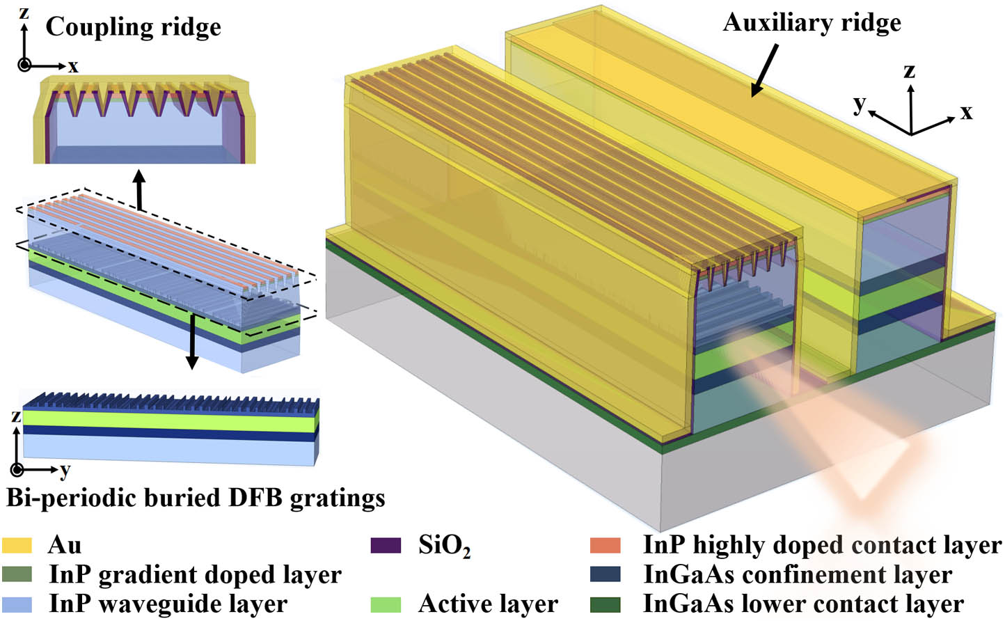
Fig. 1. Three-dimensional device structure diagram of coupled ridge dual-wavelength DFB QCL.

Fig. 2. (a) Electroluminescence spectrum of the materials. Δ E 1 Δ E 2 λ 1 σ = 0.5 λ 2 σ = 0.6 1 (c).
Fig. 3. Dependences of supermode loss and loss difference on (a) ridge period and (b) array etching depth at λ 1 = 7.5 μm λ 1 = 7.05 μm λ 1 = 7.5 μm
Fig. 4. (a) Cross-sectional photographs of the actual coupling ridge portions for parameter sets 1 (left) and 2 (right). (b) Cross-sectional photograph of actual device mounted epi-side down onto the graphite heat-sink.
Fig. 5. (a) L - I - V T sink W S 1 = 7.5 μm J t h T J th = J 0 exp ( T / T 0 ) L - I - V T sink W S 2 = 8.9 μm
Fig. 6. Far-field profile along the ridge width direction at room temperature for a device with ridge period P 1 = 9.5 μm W S 1 = 7.5 μm D 1 = 2.3 μm λ 2
Fig. 7. (a) Optical spectra measured by varying the current at room temperature (20°C). (b) Emission spectra of the device during operation when T − 4 ° C 1.05 × I th λ 1 λ 2


Set citation alerts for the article
Please enter your email address

© Copyright 2018-2021 | Chinese Laser Press. All Rights Reserved 沪ICP备15018463号-20