1Key Laboratory of Semiconductor Materials Science, Institute of Semiconductors, Chinese Academy of Sciences, Beijing Key Laboratory of Low Dimensional Semiconductor Materials and Devices, Beijing 100083, China
2Center of Materials Science and Optoelectronics Engineering, University of Chinese Academy of Sciences, Beijing 100049, China
To facilitate the development of on-chip integrated mid-infrared multi-channel gas sensing systems, we propose a high-power dual-mode (7.01 and 7.5 μm) distributed feedback quantum cascade laser based on stacked 3D monolithic integration. Longitudinal mode control is achieved by preparing longitudinal nested bi-periodic compound one-dimensional Bragg gratings along the direction of the cavity length in the confinement layer. Additionally, transverse coherent coupling ridges perpendicular to the cavity length direction are fabricated in the upper waveguide layer to promote the fundamental transverse mode output when all ridges are in phase. Stable dual-wavelength simultaneous emission with a side-mode suppression ratio of more than 20 dB was achieved by holographic exposure and wet etching. The entire spectral tuning range covers nearly 100 nm through joint tuning of the injection current and heat-sink temperature. High peak power and beam quality are guaranteed by the parallel coherent integration of seven-element ridge arrays. The device operates in a fundamental supermode with a single-lobed far-field pattern, and its peak output power reaches 3.36 W in pulsed mode at 20°C. This dual-mode laser chip has the potential for in-situ on-chip simultaneous detection of and gases in leak monitoring.
1. INTRODUCTION
In recent years, extensive research has been conducted on quantum cascade lasers (QCLs) for operation in the mid-infrared spectral region with dense gas molecular absorption lines [1–4]. Trace gases within the QCL spectral coverage, such as , , , and , have gained significant attention for environmental monitoring [5], medical analysis [6], and in-situ atmospheric detection of the Earth and other planets [7,8]. Taking the application in the fields of oil and natural gas as an example, detecting the intensity ratio of and is necessary to diagnose natural gas pipeline leakage by determining whether the measured leaking gas is from natural gas, underground biogas, or other combustible gases [9]. In these cases, multiple gases must often be detected simultaneously [7,10]. At present, to avoid carrying multiple lasers [11,12], the simultaneous detection of multiple gases mainly relies on wavelength scanning (laser array) [13] absorption spectroscopy. Furthermore, remote detection and other applications also require high output power and a low divergence angle. Recently, Karnik et al. reported on the applicability of arrayed waveguide gratings (AWGs) in mid-infrared InGaAs/InP material platforms for effective wavelength beam combinations [14], which demonstrates the feasibility of applying the inverse process for wavelength division to implement multi-channel gas sensing through a passive waveguide. By this way, to achieve high-precision on-chip spectral detection of multiple gases, the input terminal must have dual- or multi-mode operation with a high side-mode suppression ratio (SMSR) at the target absorption lines, in addition to high beam quality and high output power.
These goals fundamentally require effective regulation of both the longitudinal and transverse modes of QCLs while increasing their output power. To achieve frequency-specific longitudinal mode outputs, distribution feedback (DFB) gratings are introduced into the upper confinement layer or surface [15,16]. Optimized multi-core materials, sampling gratings, and compound grating preparation are adopted to realize multiple frequency-specific longitudinal mode outputs with a high SMSR in a single laser [17–20]. Note that most of the above approaches with DFB gratings degrade the output power because of the influence of grating coupling strength [2,21,22]. Larger output power can be extracted by increasing the gain volume [23,24]. Simply increasing the ridge width, however, in turn generates higher-order transverse mode and deteriorates the beam quality in the form of the multi-lobe far field [25]. Photonic-crystal structures and coherent control via radio-frequency injection have been investigated in recent years for suppressing higher-order transverse modes [26,27]. The phase locking of the optical field between integrated ridge array elements is another valuable way to balance high power and lateral mode control [28,29]. Nevertheless, achieving the aforementioned requirements in a single device remains an engineering challenge owing to the presence of trade-offs and competing optimization goals.
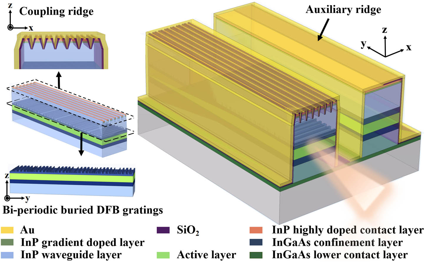
In this work, we demonstrate a tunable dual-wavelength ( of μ and of μ) QCL with high beam quality and high output power, which is based on a three-dimensional (3D) stacked monolithic integration solution. Along the direction of the cavity length, bi-periodic composite buried DFB gratings achieve dual frequency-specific longitudinal mode selection. The ridge array is arranged along the direction of ridge width, and coherent coupling forms a transverse fundamental mode while increasing the effective ridge width to improve output power. The structures are stacked on one ridge along the growth direction and fabricated in the upper confinement layer and the upper waveguide layer. The laser based on this technology maintains a stable dual longitudinal mode operation during temperature tuning from to 60°C, and the temperature tuning coefficients for and are and , respectively. By combining current and temperature tuning, the device can cover a spectral range of nearly 100 nm. A single-lobe far-field mode was maintained over most of the driving current dynamic range, with a full width at half-maximum (FWHM) ranging from 10.6° to 13.2°. At 20°C, the peak output power of the device with a cavity length of 2 mm reaches 3.36 W.
Sign up for Photonics Research TOC. Get the latest issue of Photonics Research delivered right to you!Sign up now
2. DESIGN AND FABRICATION
According to the mid-infrared characteristic absorption of the target gases (, , and ), we set the working wavelength around 7 μm in this work.
A bound-to-continuous state transition is introduced into the active region design, which is composed of a 50-stage strain compensated material system. The specific layer thickness sequence of the active region in a single period from the injection barrier is given as follows: 1.8/3.9/1.0/4.7/0.9/5.06/0.9/1.7/4/2.6/2.8/2.7/1.9/2.8/1.7/3.2 (nm), where the barrier layers are shown in bold, the wells are normal, and the -doped layers (Si, ) are underlined. The transition matrix elements from the upper level to the two lower levels in this material structure are 1.42 and 1.38 nm, respectively, and thus the transition to lower levels can be achieved. Moreover, multiple energy levels in the injection region form quasi-continuous injection into the upper level, preventing the energy levels from staggering sensitively with increasing voltage. Thus, the gain spectrum can be broadened effectively over a large voltage range. This ensures that the gain linewidth for multiple wavelengths remains within the large current tuning range to achieve simultaneous emission of multi-wavelengths.
The active region and InGaAs confinement layers were grown by molecular beam epitaxy, and the InP cladding was regrown by metal-organic vapor phase epitaxy (MOVPE). Starting from the semi-insulating (SI) InP substrate, the epitaxial structure is shown in Fig. 1: the high doping lower contact layer (0.2 μm, Si, ), InP bottom waveguide layer (5 μm, Si, ), confinement layer (200 nm, Si, ), active region, confinement layer (300 nm, Si, ), InP upper waveguide layer (3 μm, Si, ), InP gradient-doped layer (150 nm, Si, to ), and InP highly doped contact layer (850 nm, Si, ) are grown sequentially.
A. Bi-Periodic Compound Gratings for Longitudinal Mode Control
Figure 2(a) shows the electroluminescence (EL) spectrum of the material, which contains two gain peaks with a significant overlap. To approach the maximum gain value and consider the waveguide loss difference caused by the free carrier absorption, is selected near the gain center, and is selected to be tens of wavenumbers blue-shifted relative to the higher gain peak position. These wavelengths satisfy the requirements for each mode to be close to the maximum value of its corresponding gain peak and ensure a sufficient gain bandwidth to achieve simultaneous lasing. In addition, the lasing peak should encompass the signals of multiple gases. After comprehensive consideration, the final wavelengths were defined as μ and μ.
Figure 2.(a) Electroluminescence spectrum of the materials. and represent the gain spectra from the upper energy level to the two lower energy levels, respectively. (b) Coupling coefficient varies with the grating duty cycle and grating depth for the two wavelengths. The upper insets show the calculated modal profiles of emission with (left) and emission with (right), respectively. (c) Schematic diagram of bi-period grating formed by different photolithographic stripes. (d) The propagation waves correspond to the gratings of the same color in Fig. 1(c).
The first-order grating periods are selected as μ and μ, which satisfy the Bragg condition for lasing at μ and μ, respectively. As demonstrated in Fig. 1, the buried gratings are prepared in the upper confinement layer. To realize dual-wavelength lasing, the coupling coefficients at the two wavelengths must be similar. From Fig. 2(b), similar coupling coefficients are obtained when the grating depth is 120 nm, and the grating duty cycles values of and are 0.5 and 0.6, respectively.
Bi-periodic compound gratings nested within each other were fabricated by wet etching after two consecutive holographic exposures. The etching morphologies of the single-period and bi-periodic gratings are shown in Fig. 2(c). The longitudinal mode selection mechanisms of the superimposed double gratings are independent of each other. The corresponding propagation wave of grating 1 [shown as the gray curve in Fig. 2(d)] can be expressed as , where is the distance from the cavity surface along the cavity length direction. The grating formed by the second holographic exposure [shown as the red curve of Fig. 2(d)] forms an uncertain initial phase relative to grating 1 because of the spatial position offset . The propagation wave corresponding to this grating can be simply expressed as . Finally, the propagating waves in the superimposed composite grating [shown in the blue pattern in Fig. 2(d)] can be expressed as . From the sum function operation of the trigonometric function, it is known that the period of is the least common multiple of and , independent of . That is, the spatial position offset of two gratings only affects the initial phase of the interference wave and does not affect the mode selection mechanism. This method can be extended to more wavelengths. And it is worth noting that higher etching accuracy is required when the number of wavelengths is increased.
B. Coherent Coupling Ridge Array for Optimizing Transverse Mode and High Output Power
The coherent coupling ridge can provide transverse mode control under the premise of high output power. The design of coherent ridge arrays is mainly related to three parameters: etching depth , period of ridge , and width of single ridge . The coupling ridge structure is confined to the upper InP waveguide layer and does not reach the active region, so this etching depth ensures that different ridge waveguides share only one active region. It avoids a low coupling coefficient being caused by the independence of the active regions of the coherent arrays and contributes to improved far-field beam quality. At the same time, it also avoids the problem of insufficient refractive index contrast between the etched and non-etched regions originating from small etching depth . Moreover, to promote the formation of fundamental supermodes, it is necessary to concentrate the mode intensity under the ridge waveguide to enhance the coupling between adjacent ridges. Therefore, the ridge width should be as large as possible under the determined ridge period .
The mode selection mainly depends on the mode waveguide loss difference [29]. The corresponding waveguide absorption loss was then calculated after obtaining the complex refractive index for different modes. and can be expressed as where is the vacuum wave vector. The order of magnitude of is , and the loss is extremely sensitive to changes in . Therefore, the loss difference value is only indicative, and the actual is mainly determined by the practical lateral corrosion degree of wet corrosion. Here, the effects of ridge period and etching depth on supermode loss are simulated and discussed (taking as an example, and a similar analysis was conducted on ). The simulation results of indicate that, although a smaller ridge period is beneficial for obtaining an in-phase fundamental supermode, the waveguide loss is relatively high [Fig. 3(a)]. The excessively large period may only satisfy higher-order supermodes. Moreover, a low etching depth may be insufficient to produce the fundamental supermode, and the excessive etching depth leads to a large loss [Fig. 3(b)]. Carrying out the same analysis on , the final ridge period and the etching depth should be kept within 9–11 and 2.3–2.45 μm, respectively, to ensure a large mode loss difference and a low fundamental supermode loss. The fundamental supermode near-field profiles of the seven-element coupled ridge waveguide structure at 7.05 and 7.5 μm are shown in Figs. 3(c) and 3(d), respectively. The field strength is concentrated in the center of the active area, indicating the in-phase operation in each ridge element.
Figure 3.Dependences of supermode loss and loss difference on (a) ridge period and (b) array etching depth at μ. Fundamental supermode near-field profiles of the seven-element coupled ridge waveguide structure at (c) μ and (d) μ calculated using COMSOL finite element method software.
In the practical chip process, the upper waveguide layer of InP was removed down to the first InGaAs layer, using concentrated HCl as a selective wet etch solution. First-order Bragg gratings for were exposed by optical lithography, then the turning platform of the holographic exposure system was shifted to the angle corresponding to , and the exposure time was decreased to prepare the grating 2 with . After using a photomask where the grating patterns had been defined on the InGaAs confinement layer by wet etching, then the upper InP layers were regrown over the gratings using MOVPE. After secondary epitaxy, coupling ridge arrays were prepared by lithography and wet chemical etching. Parameters chosen for the actual coupling ridge structures 1 and 2 are shown in Fig. 4(a). As an SI InP substrate is used in this device, the coplanar electrode design is adopted. To improve the heat dissipation capability of the device, the laser is mounted epi-side down on an AlN submount. In this way, the auxiliary ridge must cooperate with the graphite heat sink, as shown in Fig. 4(b), to achieve the purpose of leading wires from the electrode. So, we alternately etched and smoothed the corrosion interface until the lower contact layer of InGaAs was exposed to form an auxiliary ridge acting as an electrode on the same surface. Subsequently, an insulation layer of film was deposited, which left an electric injection window formed by dry etching, and electrical contact was provided by a Ti/Au layer deposited through electron beam evaporation. An additional 5-μm-thick gold layer was electroplated to further improve the heat dissipation. After being thinned down, the final device structure is shown in Fig. 1. We combined the coupled ridges along the ridge width direction for transverse mode control and the bi-period composite gratings along the cavity length direction for longitudinal mode selection. The two are, respectively, located on the upper confinement layer and the upper waveguide layer in the material growth direction .
Figure 4.(a) Cross-sectional photographs of the actual coupling ridge portions for parameter sets 1 (left) and 2 (right). (b) Cross-sectional photograph of actual device mounted epi-side down onto the graphite heat-sink.
The device was characterized using a thermoelectric cooler. The spectra were measured by Fourier transform infrared spectroscopy in rapid scanning mode, with a resolution of . The emitted optical power was measured using a calibrated thermopile detector placed in front of the laser.
We present the light power-current-voltage () characteristics of a seven-element coupled ridge array with a cavity length of 2 mm, ridge period () of 9.5 μm, and single ridge width () of 7.5 μm (total coupled ridge width μ) at a driving repetition rate of 10 kHz and a pulse width of 1 μs. Typical characteristics at different heat-sink temperatures ranging from 10°C to 40°C are shown in Fig. 5(a). At 20°C, the threshold currents are 1.4 A () for (7.5 μm) and 2.2 A () for (7.01 μm). A peak output power up to 3.36 W was obtained under dual-mode operation with a slope efficiency of 0.798 W/A and a wall plug efficiency of 3.11%. To prevent damage, the maximum operating current was not evaluated.
Figure 5.(a) curves at from 10°C to 40°C for a 2-mm-long QCL with ridge width μ. The inset shows as a function of in pulsed mode. The dashed line is the fitting result obtained using the exponential function . (b) curves at from 20°C to 40°C for a 2-mm-long QCL with ridge width μ.
Apart from devices of size 1, we also prepared another seven-element coherent ridge array 2 for comparison, with a total coupled ridge width of 90 μm. It is generally accepted that the device output power increases with increasing ridge width, and the supermode loss of size 1 at the two wavelengths is smaller than that of size 2 in the theoretical simulations. However, the measured peak output power does not increase significantly, as shown in Fig. 5(b). Simultaneously, the device threshold becomes higher. Moreover, even for size 1 devices with longer cavity lengths of 3 mm, the power does not increase with an increasing cavity length. Based on the phenomena discussed above, we consider that the heat accumulation in the active regions is greater than that of size 1 with 2 mm cavity length, which is unfavorable for output power enhancement. In addition, the waveguide loss caused by side wall roughness in the coupled ridge array is a potential reason for the increased device threshold and limited output power. Therefore, the coherent coupled ridge structure cannot reach high powers by simply increasing the active region volume, even if it meets the requirements for the fundamental supermode in the simulations.
The far-field patterns of the laser arrays in the ridge width direction are of the most concern. The diffraction limit angles calculated for a 75-μm-wide aperture array are and at μ and μ, respectively. The far-field distribution along the ridge width direction under the influence of the coherence between the interval emission regions was measured at a driving repetition frequency of 3 kHz and a pulse width of 1 μs. As shown in Fig. 6(a), single-wavelength lasing was measured before the dual-mode operation was triggered, and the devices showed single-lobe far-field distributions along the ridge width direction. The FWHM of the far-field pattern is 4.9° when , and the FWHM is close to . Figure 6(b) shows the far-field distribution under the dual-mode operation at room temperature. The FWHMs of the far-field pattern range from 10.6° to 13.2°, corresponding to and for the dominant wavelength at the time, respectively. These results indicate that the operations are in phase in each ridge unit at different currents.
Figure 6.Far-field profile along the ridge width direction at room temperature for a device with ridge period μ, ridge width μ, and depth μ. (a) Before lasing. (b) Lasing at dual wavelengths. Data fittings performed using the Gaussian function are represented by solid lines.
It should be noted that, as the driving current continues to increase (e.g., for ), the high-order supermode acquires sufficient gain, and side lobes gradually appear symmetrically outside the center, which primarily appeared at angles of and . According to Fraunhofer’s multiple slit diffraction model, the total far-field intensities of the phase-locked array represent the joint effects of single-emitter diffraction and interference from periodically spaced emitters [30]. The interference distribution of the bright stripes is determined by the following equation: where is the ridge period, is the diffraction angle, and is the phase shift between adjacent ridges. In our example, is 9.5 μm (), and when , and , the calculated values for μ are 0°, , and , and the values for μ are 0°, , and , respectively. These calculated values are consistent with the experimental results. Based on the discussion above, we consider the high-order supermode with the phase shift to be the cause of the FWHM increase in the far-field center lobe. The FWHM of the side lobe at is 7.14°, which is similar to 7.007° for . This indicates that the high-order supermode with the phase shift contributes to the appearance of these side lobes. These results demonstrate that a large ridge width inevitably causes the higher-order mode to be excited at high currents, and the difference in loss between the fundamental supermode and the higher-order mode is insufficient to provide a pure fundamental supermode. However, the power is still obviously concentrated within the center lobe, which remains high for applications that require high power but do not have strict far-field requirements.
To characterize the lasing characteristics of the dual-mode QCL more clearly, we first tested the driving current tuning spectra of the device above the threshold at 20°C, with results shown in Fig. 7(a). When the injection current ranges from 1.4 to 2.2 A, the laser presents only single-mode lasing, and when the injection current exceeds 2.2 A and is within a large dynamic range, the dual wavelengths of the QCL can be simultaneously lasing. In addition, because the device threshold current increases with increasing temperature, we measured the temperature-tunable spectra under the condition that single-mode lasing was ensured at the two wavelengths. As shown in Fig. 7(b), the change in lasing wavelength with temperatures from at to at 60°C was obtained with a temperature tuning coefficient of . For , the wavelength changed from 1428.151 to with a tuning coefficient of within the same temperature range. As indicated in the insets of Fig. 7(c), an SMSR exceeding 20 dB was achieved for and . In addition, during temperature tuning, both wavelengths maintained stable tuning without any mode hopping.
Figure 7.(a) Optical spectra measured by varying the current at room temperature (20°C). (b) Emission spectra of the device during operation when was varied from to 60°C in increments of 4°C (measured at ). The insets show the linearly fitted tuning characteristics of lasing frequency versus injection temperature. (c) The upper part, spectrum of the tuning range combined with temperature and current tuning. The insets are single-mode spectra of the and emissions at 20°C with SMSR of over 20 dB. The lower part, the absorption lines of gas molecules within the tuning range.
Increases in temperature and current cause the lasing wavelength to be red-shifted linearly; therefore, a combination of current tuning and temperature tuning can broaden the tuning range. As depicted in the upper part of Fig. 7(c), the spectra can cover (60°C, 4 A) to (, 1.5 A) and (60°C, 4 A) to (, 2.3 A). The total tuning range reaches approximately 100 nm. The temperature and current conditions corresponding to each wavelength can be determined via measurements. In the lower part of Fig. 7(c), the laser covers the spectrum for the molecular absorption lines of multiple gases, such as and , whose molecular absorption lines do not overlap [11]. It can also be used for the simultaneous detection of and to improve methane leakage detection [31].
4. CONCLUSION
In conclusion, using superimposed buried bi-periodic DFB gratings and a coupled ridge array, we demonstrate a stacked 3D monolithic integrated dual-mode QCL with high peak output power. A seven-element QCL array was simulated and fabricated to explore the coherence of the coupled ridge waveguide structures. It was observed that the far-field distribution of the main lobe remained stable in the ridge width direction during dual-wavelength lasing. The peak output power reached up to 3.36 W at 20°C. With current or temperature tuning processes, the device maintained mutually independent double longitudinal modes without mode hopping, and the temperature tuning coefficients were and at and , respectively. By combining the current and temperature tuning modes, the whole spectrum can cover nearly 100 nm. The wide optical coverage, high output power, and beneficial single-lobe far-field distribution of this QCL are advantageous for practical application in high-resolution multi-gas detection (, , , etc.) and medical analysis. Further research can be combined with the AWG structure on the InGaAs/InP material platform. By pumping the single laser, a multi-wavelength high-power integrated laser source with high beam quality is obtained to detect more gases.
Acknowledgment
Acknowledgment. The authors thank Ping Liang for her help in device processing.
[8] J. Sinclair, P. G. J. Irwin, E. Wilson, S. Calcutt. Detectability of trace gases in the Martian atmosphere using gas correlation filter radiometry. European Planetary Science Congress, EPSC2015-376(2015).