Peng Zhu, Lei Xiao, Tai Sun, Haofei Shi. Research progress of micro-nano structures enhanced infrared detectors (Invited)[J]. Infrared and Laser Engineering, 2022, 51(1): 20210826
Search by keywords or author
- Infrared and Laser Engineering
- Vol. 51, Issue 1, 20210826 (2022)
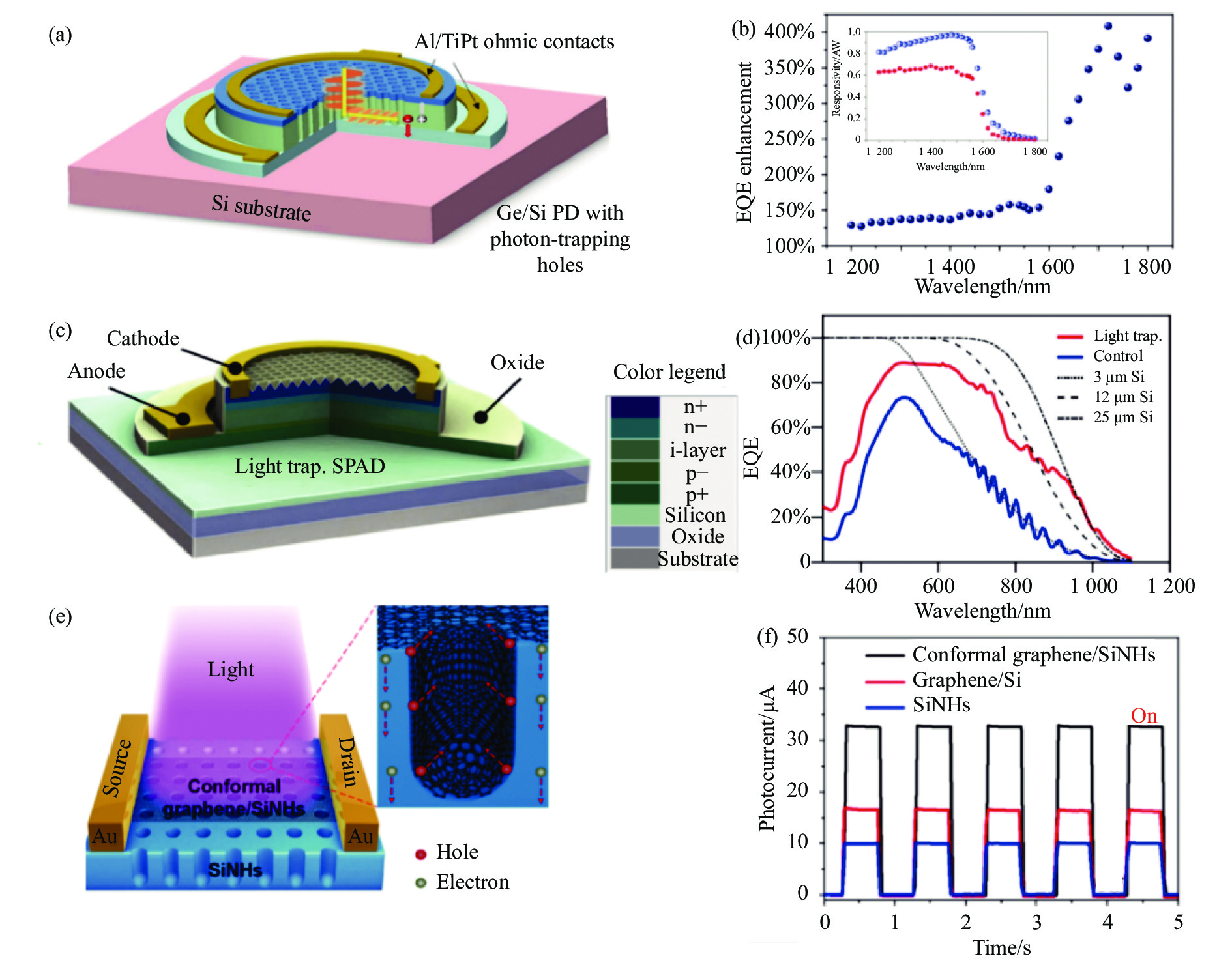
![Infrared detectors with micro-holes on silicon substrates[19-21]; (a) Schematic diagram of Si-Ge optoelectronic device with micro-hole array structures[19]; (b) External quantum efficiency enhancement coefficient and responsivity in the 1 200-1 800 nm band of the Si-Ge device[19];(c) Schematic diagram of a silicon single-photon avalanche detector with micro-hole array structures[20]; (d) External quantum efficiency of devices of different sizes[20]; (e) Schematic diagram of conformal graphene/silicon nanopore detector[21] ; (f) Photoelectric response of silicon nanopore, graphene/silicon and conformal graphene/silicon nanopore detectors[21]](/richHtml/irla/2022/51/1/20210826/img_1.jpg)
Fig. 1. Infrared detectors with micro-holes on silicon substrates[19-21]; (a) Schematic diagram of Si-Ge optoelectronic device with micro-hole array structures[19]; (b) External quantum efficiency enhancement coefficient and responsivity in the 1 200-1 800 nm band of the Si-Ge device[19];(c) Schematic diagram of a silicon single-photon avalanche detector with micro-hole array structures[20]; (d) External quantum efficiency of devices of different sizes[20]; (e) Schematic diagram of conformal graphene/silicon nanopore detector[21] ; (f) Photoelectric response of silicon nanopore, graphene/silicon and conformal graphene/silicon nanopore detectors[21]
![(a) A schematic diagram of a silicon photodiode integrated with a micro-holes[22]; (b) SEM images of holes of different shapes integrated in the photodiode, including square holes, hexagonal holes, cylindrical and funnel shapes[22]; (c) Scanning electron microscope picture of the active area of the photodiode[22]; (d) A schematic diagram of a silicon photodetector with integrated micro structures[23]; (e) Top and cross-sectional views of the funnel-shaped and inverted pyramid-shaped light trapping structures[23]; (f) Relationship between the external quantum efficiency and the number of nano-holes[23]](/richHtml/irla/2022/51/1/20210826/img_2.jpg)
Fig. 2. (a) A schematic diagram of a silicon photodiode integrated with a micro-holes[22]; (b) SEM images of holes of different shapes integrated in the photodiode, including square holes, hexagonal holes, cylindrical and funnel shapes[22]; (c) Scanning electron microscope picture of the active area of the photodiode[22]; (d) A schematic diagram of a silicon photodetector with integrated micro structures[23]; (e) Top and cross-sectional views of the funnel-shaped and inverted pyramid-shaped light trapping structures[23]; (f) Relationship between the external quantum efficiency and the number of nano-holes[23]
Fig. 2. [in Chinese]
Fig. 3. Mid-wave infrared detector samples of HgCdTe with microstructures of different filling factors[24]
Fig. 4. Structure and photoelectric characteristics of different types of nanorods near infrared photodetectors[26-29]. (a) I -V curve of the SiNW/Au/Graphene detector and the device structure[26]; (b) Schematic diagram of the silicon nanowire array/perovskite photodetector(cross-sectional view and 850 nm incident light time response curve under zero bias)[27]; (c) Schematic diagram of PbSe2/GeNcs array heterojunction photodetector(cross-sectional SEM image of germanium nanocone array and I -V curve diagram)[28]; (d) Schematic diagram of the ZnO/MoS2detector(SEM images and time-current response)[29]
Fig. 5. Structures and performances of enhanced infrared detectors with different types of surface metal microstructures[34-37]. (a) Structure diagram of the aysmmetric infrared plasma detector(SEM image and electric field intensity enhancement coefficient)[34] ; (b) Schematic diagram of the two-color infrared detector with cross stars(SEM image and reflection curve)[35];(c) Schematic diagram of the square-hole plasma long-wave infrared detector(SEM image and curve of absorption enhancement factor)[36]; (d) Schematic diagram of the plasma cavity quantum well infrared detector(SEM image and absorption enhancement spectrum)[37]
Fig. 6. Structures and performance of several types of hot-electron infrared detectors with metal meta-surface[43-46]. (a) Structure diagram, SEM image and photoelectrical properties of local plasmon thermal electron injection photodetector[43]; (b) Structure diagram and quantum efficiency curve of plasmon thermoelectron photodetector based on surface plasma[44]; (c) Schematic diagram and spectral response of all-silicon thermoelectronic photodetector[45]; (d) Structure diagram and absorption curve of a wide band thermo-electron photodetector[46]
Fig. 7. Structures and performance of several types of 3D plasmonic cavity enhanced infrared detectors with micro-structure[50-53]
Fig. 8. Structures and performance of plasmonic cavity enhanced 2D materials infrared detectors with micro-structure [54-56]. (a) Schematic diagram of plasma cavity structure and absorption curve of graphene[54]; (b) Schematic diagram and absorption curve of hybrid grating Fabry-Perot structure integrated with graphene film[55]; (c) Schematic diagram of gold nanostructure plasmonic cavity and absorption curve of black phosphorus[56]
Fig. 9. Structures and performance of three kinds of heavily doped semiconducting plasma detectors[61-63]. (a) Structures of heavily doped plasmonic detector, distribution of electrical field and curve of EQE[61]; (b) Schematic diagram of ultra-thin enhanced absorption long-wave infrared detector(band-structure schematics and the absorption curve)[62] ; (c) Schematic diagram of a single-cycle GMR detector (Scanning electron micrographs and detectability curves of cross-sections)[63]
Fig. 9. [in Chinese]
| ||||||||||||||||||||||||||||||||||||||||||||||||
Table 1. Classification and progress of micro-nano structure enhanced infrared detectors

Set citation alerts for the article
Please enter your email address


