• Photonics Research
  • Vol. 5, Issue 4, 305 (2017)
Md Rezwanul Haque Khandokar1、2、*, Masuduzzaman Bakaul1、3, Md Asaduzzaman1、2, Stan Skafidas1, and Thas Nirmalathas1
Author Affiliations
  • 1Department of Electrical and Electronic Engineering, The University of Melbourne, Parkville, VIC 3010, Australia
  • 2Data 61/Commonwealth Scientific and Industrial Research Organisation, Parkville, VIC 3052, Australia
  • 3School of Engineering, Monash University Malaysia, 47500 Bandar Sunway, Selangor, Malaysia
  • show less
    DOI: 10.1364/PRJ.5.000305 Cite this Article Set citation alerts
    Md Rezwanul Haque Khandokar, Masuduzzaman Bakaul, Md Asaduzzaman, Stan Skafidas, Thas Nirmalathas. Characterization of geometry and depleting carrier dependence of active silicon waveguide in tailoring optical properties[J]. Photonics Research, 2017, 5(4): 305 Copy Citation Text show less
    (a) Primary geometry of the active Si waveguide under investigation. (b) Layout with specified doping regions.
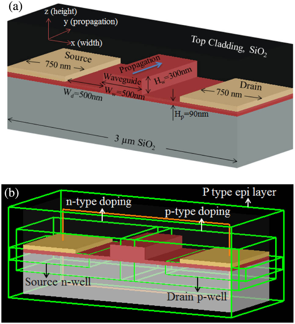
    Fig. 1. (a) Primary geometry of the active Si waveguide under investigation. (b) Layout with specified doping regions.
    Functionality of the waveguide: (a) confinement of TE polarized light; (b) electrostatics at −4 V bias voltage.
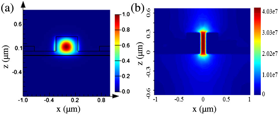
    Fig. 2. Functionality of the waveguide: (a) confinement of TE polarized light; (b) electrostatics at 4  V bias voltage.
    Carrier distribution (n-type) as a function of applied bias (a) at zero bias voltage, (b) at V=−2 V, (c) at V=−4 V.
    Fig. 3. Carrier distribution (n-type) as a function of applied bias (a) at zero bias voltage, (b) at V=2  V, (c) at V=4  V.
    Changes of waveguide parameters with respect to the changes in bias voltage and uniform doping concentration: (a) real RI versus bias voltage; (b) imaginary RI versus bias voltage; (c) ML versus bias voltage; and (d) Δn versus doping concentration.
    Fig. 4. Changes of waveguide parameters with respect to the changes in bias voltage and uniform doping concentration: (a) real RI versus bias voltage; (b) imaginary RI versus bias voltage; (c) ML versus bias voltage; and (d) Δn versus doping concentration.
    Changes of waveguide parameters with respect to the changes in bias voltage and nonuniform doping concentration: (a) real RI versus bias voltage; (b) imaginary RI versus bias voltage; (c) ML versus bias voltage; and (d) Δn versus doping concentration.
    Fig. 5. Changes of waveguide parameters with respect to the changes in bias voltage and nonuniform doping concentration: (a) real RI versus bias voltage; (b) imaginary RI versus bias voltage; (c) ML versus bias voltage; and (d) Δn versus doping concentration.
    Changes of waveguide parameters with respect to the changes in bias voltage and Hp: (a) real (RI) versus bias voltage; (b) img (RI) versus bias voltage; (c) ML versus bias voltage; and (d) Δn versus doping concentration.
    Fig. 6. Changes of waveguide parameters with respect to the changes in bias voltage and Hp: (a) real (RI) versus bias voltage; (b) img (RI) versus bias voltage; (c) ML versus bias voltage; and (d) Δn versus doping concentration.
    Confinement of the mode for different Hp: (a) Hp=50 nm, (b) Hp=120 nm.
    Fig. 7. Confinement of the mode for different Hp: (a) Hp=50  nm, (b) Hp=120  nm.
    Changes of waveguide parameters with respect to the changes in bias voltage and Wd: (a) imaginary RI versus bias voltage; (b) ML versus bias voltage.
    Fig. 8. Changes of waveguide parameters with respect to the changes in bias voltage and Wd: (a) imaginary RI versus bias voltage; (b) ML versus bias voltage.
    E-field intensity (in log scale) of the confined mode for different Wd: (a) Wd=300 nm; (b) Wd=700 nm.
    Fig. 9. E-field intensity (in log scale) of the confined mode for different Wd: (a) Wd=300  nm; (b) Wd=700  nm.
    Changes of waveguide parameters with respect to the changes in bias voltage and Ww: (a) real RI versus bias voltage; (b) imaginary RI versus bias voltage; (c) ML versus bias voltage; and (d) Δn versus doping concentration.
    Fig. 10. Changes of waveguide parameters with respect to the changes in bias voltage and Ww: (a) real RI versus bias voltage; (b) imaginary RI versus bias voltage; (c) ML versus bias voltage; and (d) Δn versus doping concentration.
    Changes of waveguide parameters with respect to changes in bias voltage and cladding material: (a) real RI versus bias voltage; (b) imaginary RI versus bias voltage; (c) ML versus bias voltage; and (d) Δn versus doping concentration.
    Fig. 11. Changes of waveguide parameters with respect to changes in bias voltage and cladding material: (a) real RI versus bias voltage; (b) imaginary RI versus bias voltage; (c) ML versus bias voltage; and (d) Δn versus doping concentration.
    Changes of waveguide parameters with respect to the positive bias voltage and nonuniform changes in doping concentration: (a) real RI versus bias voltage; (b) imaginary RI versus bias voltage; (c) ML versus bias voltage; and (d) Δn versus doping concentration.
    Fig. 12. Changes of waveguide parameters with respect to the positive bias voltage and nonuniform changes in doping concentration: (a) real RI versus bias voltage; (b) imaginary RI versus bias voltage; (c) ML versus bias voltage; and (d) Δn versus doping concentration.
    Field profile of the confined mode with (a) no bend, (b) bending the waveguide in upward direction with 5 μm bend radius, (c) bending in right direction with 10 μm bend radius, (d) bending in downward direction with 5 μm bend radius.
    Fig. 13. Field profile of the confined mode with (a) no bend, (b) bending the waveguide in upward direction with 5 μm bend radius, (c) bending in right direction with 10 μm bend radius, (d) bending in downward direction with 5 μm bend radius.
    Changes of waveguide parameters with respect to the changes in doping concentrations at −4 V bias voltage: (a) loss versus doping concentration for upward bending; (b) loss versus doping concentration for right bending; (c) loss versus doping concentration for downward bending; (d) real RI versus doping concentration; (e) Δn versus doping concentration; (f) dispersion versus wavelength.
    Fig. 14. Changes of waveguide parameters with respect to the changes in doping concentrations at 4  V bias voltage: (a) loss versus doping concentration for upward bending; (b) loss versus doping concentration for right bending; (c) loss versus doping concentration for downward bending; (d) real RI versus doping concentration; (e) Δn versus doping concentration; (f) dispersion versus wavelength.
    Confinement of TM polarized light.
    Fig. 15. Confinement of TM polarized light.
    Changes of waveguide parameters for TM polarization with respect to the changes in bias voltage and nonuniform doping concentration: (a) real RI versus bias voltage; (b) imaginary RI versus bias voltage; (c) ML versus bias voltage; and (d) Δn versus doping concentration.
    Fig. 16. Changes of waveguide parameters for TM polarization with respect to the changes in bias voltage and nonuniform doping concentration: (a) real RI versus bias voltage; (b) imaginary RI versus bias voltage; (c) ML versus bias voltage; and (d) Δn versus doping concentration.
    Md Rezwanul Haque Khandokar, Masuduzzaman Bakaul, Md Asaduzzaman, Stan Skafidas, Thas Nirmalathas. Characterization of geometry and depleting carrier dependence of active silicon waveguide in tailoring optical properties[J]. Photonics Research, 2017, 5(4): 305
    Download Citation