Md Rezwanul Haque Khandokar, Masuduzzaman Bakaul, Md Asaduzzaman, Stan Skafidas, Thas Nirmalathas. Characterization of geometry and depleting carrier dependence of active silicon waveguide in tailoring optical properties[J]. Photonics Research, 2017, 5(4): 305
Copy Citation Text
Changes in refractive index and the corresponding changes in the characteristics of an optical waveguide in enabling propagation of light are the basis for many modern silicon photonic devices. Optical properties of these active nanoscale waveguides are sensitive to the little changes in geometry, external injection/biasing, and doping profiles, and can be crucial in design and manufacturing processes. This paper brings the active silicon waveguide for complete characterization of various distinctive guiding parameters, including perturbation in real and imaginary refractive index, mode loss, group velocity dispersion, and bending loss, which can be instrumental in developing optimal design specifications for various application-centric active silicon waveguides.
In recent years, silicon (Si)-based nanophotonic technology has made unprecedented progress to develop a highly integrated electronic–photonic platform [1,2]. Si with its inherent excellent linear and nonlinear optical characteristics in the infrared region, adequate thermal conductivity, and high optical damage threshold, has the ability to be engineered to conceive and design a new class of modern photonic devices [3]. The high-index-contrast waveguide, together with the unique bandgap structure, has opted Si to be considered for various state-of-the-art optical devices for applications in electro-optic modulation, light sources, chromatic dispersion manipulation, optical filtering, optical switching, optical memory, and so forth with expected cross-sectional dimensions as low as 10’s to 100’s of nanometers (nm) [4–8]. These devices, based on the requirement of biasing, can be classified into groups of “active” and “passive,” where the active devices are required to be powered electrically, but the passive devices are free from supply of electricity of any sort.
One of the key enablers of the “powered” active Si waveguide devices is the distinct concentrations of carriers in the Si waveguide that can be achieved either by carrier injection, depletion, or accumulation process that causes perturbation in optical absorption and effective refractive indices (RI). Carrier depletion is found to be more effective over carrier injection in time and thermal responses, although either of these mechanisms can be used to achieve the desired changes in carrier concentrations [9]. These perturbations in absorption and RI eventually dictate the characteristics of any active waveguide, including mode loss (ML), group velocity dispersion (GVD), and bending loss, for which careful selection and control of the distinctive parameters involving the changes of the concentrations of carriers are extremely important.
Another important aspect of any optical waveguide is the dependence of optical properties on physical dimensions, which can be varied to manipulate most of the characteristics features as desired [10,11]. However, as the physical dimensions of the waveguide are mostly in the range of 10’s to 100’s of nm, they are sensitive to the little deviations in geometry, for which precise control of manufacturing specifications and tolerances are essential, similar to the changes of the concentrations of carriers, as mentioned earlier.
Sign up for Photonics Research TOC. Get the latest issue of Photonics Research delivered right to you!Sign up now
Although active Si waveguide-based devices are delicate in nature, significant research has been carried out in the recent past. A silicon-on-insulator (SOI) based optical modulator by carrier accumulation and injection, index modulator by carrier depletion in multiple quantum well structure, electro-optically active pin structure in photonic crystal cores, and active microring resonator with different doping positions are investigated in Refs. [12–16]. Optical switching performed by Si quasi-digital optical switch (DOS) based on reverse bias diode and active ring resonators by poled-polymer/Si slot waveguides are demonstrated in Refs. [17–19]. Control and tuning delays of slow light photonic crystal Si waveguides are discussed in Refs. [20,21]. Active spectral filtering by Si Bragg grating, nano-beam resonator and junctions are demonstrated in Refs. [22,23]. Effects of free carriers, heavy doping, and the corresponding band structure of Si, effective carrier lifetime, modulation operation, and the effects of different plasmonic active metals are investigated in Refs. [24–29]. Free carrier absorption loss and broadband variable chromatic dispersion in photonic-band electro-optic waveguides, as well as dispersion engineering in Si-based photonic crystal waveguides, are also discussed in Refs. [30–32].
Most of these demonstrations are, however, quite specific about a certain geometry and focused on realizing a particular feature only, without due considerations to the inter-dependent phenomena. Recently we have compared and thoroughly characterized the characteristic features of passive Si planar, rib, and photonic crystal waveguides in tailoring effective RI, group index, GVD, and ML [33]. This paper brings the active Si waveguide for a complete characterization of various distinctive guiding parameters, including real and imaginary RIs; change in RI, ML, GVD; bending loss by incorporating changes in physical dimensions, carrier concentrations, and bias voltages, which can be instrumental in developing optimal design specifications for various application-centric active Si waveguides.
2. FORMULATION
In a waveguide, carrier-induced changes in RI are usually governed by three key mechanisms: bandfilling, bandgap shrinkage, and free carrier concentration [34]. Bandfilling is defined by Burstein–Moss effect, where electrons from the valence band require more energy than the nominal bandgap to be optically excited due to pre-filled lower energy states of conduction band in -type semiconductors [35]. This effect is more pronounced in semiconductors with smaller effective mass and lower energy gaps. Bandgap shrinkage is caused by lowering and increasing energy in the conduction and valence band, respectively, due to the overlap and correlation effects, and is nearly independent of impurity concentrations [36]. However, optical properties are strongly affected and are demonstrated for carrier refraction achieved by variation of free carrier concentrations [37]. Unperturbed RI and the related changes, due to the change in carrier concentrations, can be calculated by utilizing the well-known Plasma–Drude model [38], as expressed below: where and are the respective densities of free electron and hole carriers, , are the respective permittivities of free space and medium, and are effective masses of electrons and holes, and are the respective mobility of electrons and holes. For large values of and , the above equation reduces to
Equation (2) can be extended to calculate the changes in RI, , and absorption coefficients, , with the assumption that complex RIs also can be calculated from the change of carrier density at any particular wavelength , as expressed below: where is the charge of electron, is the RI without perturbation, is the permittivity of free space, and are the respective mobility of electrons and holes, and are conductivity effective masses of electrons and holes, and are the change in electron and hole concentration, respectively, and is the velocity of light. For an Si waveguide and a light of 1550 nm band, the wavelengths that are central to the most of the activities of current long-haul telecommunications, Eq. (3) can be simplified as follows [39]: where and are changes in RI, and and are changes in absorption resulting from change in free and carrier concentrations, respectively. Equation (4) indicates that the contribution of the concentration of holes in changing RI is much higher than that of the concentration of electrons, which is, however, opposite in the case of the coefficient of absorption.
The allowable doping concentration, which largely defines the changes in RI, is bound by the amount of accommodative ML of the waveguide. The amount of loss, which will increase sharply with higher carrier concentrations due to elevated free carrier absorption, can be calculated from imaginary part of effective RI () as expressed below:
GVD which is a combination of material and waveguide dispersion, is defined as the rate of change of the group delay with respect to wavelength and can be calculated as follows:
3. MODELING AND CHARACTERIZATION
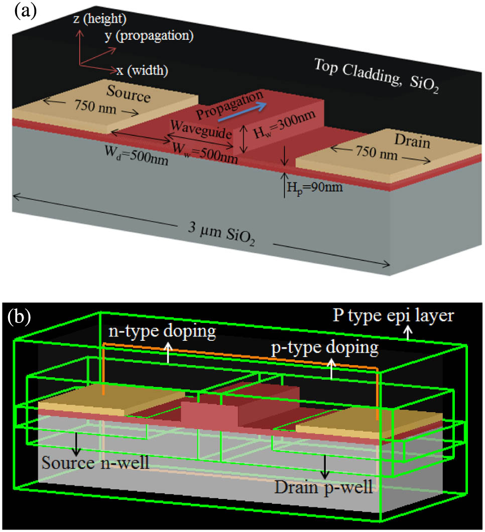
To model an active Si waveguide, a 450 nm Si layer is grown on an layer with respective width and thickness of 3 and 1 μm in virtualization, as shown in Fig. 1(a). The waveguide is chosen to be 500 nm wide. The remaining Si is etched back to 300 nm to leave a waveguide with dimensions 300 nm thick and 500 nm width that sits on an Si pad of 90 nm. The dimensions are chosen in such a way that the waveguide supports only single-mode operation at the wavelengths of 1550 nm band. At the edges, metal (Al) contacts with respective widths and thicknesses of 750 and 100 nm are grown to enable electrical biasing. The top surface of the waveguide is passivated with a thick layer of oxide.
Figure 1.(a) Primary geometry of the active Si waveguide under investigation. (b) Layout with specified doping regions.
The p-n junction is defined by using analytic profiles of diffusion-doping objects, which mimic the behavior of an ion implant. These diffusion profiles are 3D objects, where doping profiles are defined according to Gaussian or erfc analytic distribution. Dopants are supplied at the “mask-opening surface,” whereas doping concentration goes to a reference concentration at each of the other surfaces. Reference concentration is considered as , which is effectively zero concentration. At a distance of junction width, which defines the spacing from the surfaces where the analytic function is applied, dopant concentration reaches its peak value, from any surface except the source. Dopants are applied in upper surface with a junction width of 200 nm.
To enable space-charge regions, inclusion of dopants into Si is modeled by considering a background doping concentration of for a -type Si epitaxial layer, which encompasses the entire geometry. To improve the electrical contact between the metal and semiconductor, heavily doped - and -wells are used, which ensures that the contacts are ohmic. These contact wells are also defined by using the diffusion objects similar to the implants. Source -well and drain -well doping concentrations are set as and type, respectively, whereas concentrations in and waveguides are changed according to the characterization requirements discussed in different sections. Layout with the doping regions specified is shown in Fig. 1(b). Finally, to deplete the carriers across the junction, a negative bias of 0 to was applied to characterize the distinctive features.
Among different simulation platforms to model the waveguide, this investigation relied on the commercially available Lumerical Solutions [40], where the structure is designed and simulated in “Lumerical Device” to obtain electrical characteristics and then run in “Mode Solution” to obtain the effective RI and mode profiles of various waveguide modes, as explained in Ref. [41]. In a device, the steady-state solver mode is selected to perform the dc analysis with 2D y-normal solver geometry. This simultaneously solves Poisson’s equations for the electrostatic potential and drift-diffusion equations for charge where the solutions must be self-consistent. Gummel’s method is used to solve this system of equations, which decouples the charge problem from the electrostatic potential problem at each step. First, the electrostatic potential is solved holding the charge fixed; then this solution is used as a fixed input to the charge equations, and those are updated. This process continues until the solution is self-consistent. Convergence control limits the number of iterations of both Poisson and drift-diffusion solvers that may be run. Absolute tolerance of V are considered, which determines the maximum absolute change between iterations that can exist for a calculation to be considered converged. For the Poisson solver, the step converges when where is the tolerance and is the electrostatic potential. For the drift-diffusion solver, both the electron and hole quasi-Fermi levels must converge:
Figure 2(a) shows the confinement of TE single mode light, and Fig. 2(b) presents the electric field (). Carrier distribution (-type) as a function of applied bias is shown in Figs. 3(a)–3(c), where the axes denote the width, axes the height of the waveguide, and the scale bar presents the number of carriers but in logarithmic scale. It shows that, as expected, the space charge region pushes the free carrier out of the and becomes wider at higher but negative drain contact voltages.
Figure 2.Functionality of the waveguide: (a) confinement of TE polarized light; (b) electrostatics at bias voltage.
A detail characterization of various responses of depleting carriers with respect to the changes in bias voltage, doping concentration, physical dimension, and operating wavelength is undertaken as follows. All the simulations are performed for TE polarization; however, response with TM mode also investigated at the last section for comparison.
A. Uniform Doping Concentration
Figures 4(a)–4(d), respectively, show the changes in effective real and imaginary RIs, ML, and of the waveguide at the concentrations of electron () and hole () of to with a reverse bias voltage of 0 to . It shows that both carrier concentration and bias voltage have great influence on RI profiles as well as ML and of the waveguide. With a gradual increase of carrier concentrations from to , the real RIs decrease from 2.91998 to 2.919075, whereas the imaginary RIs increase from to . Similarly, gradual increase of reverse bias voltage from 0 to increases the real RI but decreases imaginary RI. Shown in Fig. 4(c), ML has increased from 5.19 to with the stipulated increase in doping concentrations, which is not, however, that pronounced for the increase of bias voltages. The dependency of on doping concentrations is also quite significant, although like ML, effects of the change in bias voltage are not that pronounced, as can be seen in Fig. 4(d).
Figure 4.Changes of waveguide parameters with respect to the changes in bias voltage and uniform doping concentration: (a) real RI versus bias voltage; (b) imaginary RI versus bias voltage; (c) ML versus bias voltage; and (d) versus doping concentration.
To utilize the benefits of higher concentrations compared with in terms of higher change in RI with lower absorption, the waveguide is characterized by varying concentration of from to , keeping the concentration of fixed to . The corresponding responses are shown in Figs. 5(a)–5(d). Similar to the characteristics of the waveguide with uniform doping shown in Figs. 4(a)–4(d), the characteristics with nonuniform doping are almost identical, except that ML is relatively smaller, and is relatively larger as expected. These differences can be further explained by the mathematical relationships shown in Eq. (4).
Figure 5.Changes of waveguide parameters with respect to the changes in bias voltage and nonuniform doping concentration: (a) real RI versus bias voltage; (b) imaginary RI versus bias voltage; (c) ML versus bias voltage; and (d) versus doping concentration.
For any active waveguide, physical dimensions also play a significant role in determining responses of the waveguide, along with the applied bias voltage and carrier concentration. Figures 6(a)–6(d) show the influence of different pad heights on real RI, imaginary RI, ML, and , respectively, where and concentrations of the waveguide are kept fixed at and , respectively, for Figs. 6(a)–6(c). For Fig. 6(d), the concentrations are varied from to to quantify the effects of changing . With an increase of pad height from 50 to 120 nm, real RI increases significantly from 2.88 to 2.96. This can be attributed to the fact that light in a waveguide with higher cross-sectional area travels a longer radial path, which causes additional phase delays and higher effective RI.
Figure 6.Changes of waveguide parameters with respect to the changes in bias voltage and : (a) real (RI) versus bias voltage; (b) img (RI) versus bias voltage; (c) ML versus bias voltage; and (d) versus doping concentration.
Higher also increases ML quite a lot, which is caused mostly by the portion of light passing through the pad area. For further clarity, confinement of the mode for 50 and 120 nm are shown in Figs. 7(a)–7(b). Shown in Fig. 6(d), thickness of has hardly any influence on , although RI and ML are influenced quite a bit.
Figure 7.Confinement of the mode for different : (a) , (b) .
D. Influence of the Gap Wd Between a Metal Contact and Waveguide
Similar to the pad height , the gap between a metal contact and waveguide also has a great influence on the overall performance of the waveguide. Figures 8(a)–8(d) show the changes in real RI, imaginary RI, ML, and , respectively, of the waveguide with at 700, 500, 400, and 300 nm, where and concentrations of the waveguide are kept fixed at and , respectively, for Figs. 8(a)–8(c) and are varied in Fig. 8(d). It shows that both imaginary RI and ML change significantly with the changes of . This change in , however, has negligible influence on real RI and , which can be attributed to the negligible effect of on changing carrier concentrations in the waveguide core.
Figure 8.Changes of waveguide parameters with respect to the changes in bias voltage and : (a) imaginary RI versus bias voltage; (b) ML versus bias voltage.
For further clarity about optimum , -field intensity of the confined mode is plotted for two values of at 300 and 700 nm, as shown in Figs. 9(a) and 9(b), respectively. Figure 9(a) shows that the confined mode struggles to be contained within the gap between the source and the drain, whereas in Fig. 9(b), it is contained perfectly. Therefore, the inadequacy of that spreads the mode over metal contacts needs to be avoided to enable smaller ML, which also is indicated by Fig. 8(c). However, larger will result in lower operational speed.
Figure 9.-field intensity (in log scale) of the confined mode for different : (a) ; (b) .
Figures 10(a)–10(c) show the changes in performance of the waveguide in real RI, imaginary RI, and ML at of 500, 700, 800, and 1000 nm with the waveguide height fixed at 400 nm, and concentrations fixed, respectively, at and , and bias voltage varied from 0 to , whereas Fig. 10(d) shows the change in with and concentrations varied from to by keeping other parameters unchanged. Similar to the responses at the changes of pad heights, increasing from 500 to 1000 nm changes real and imaginary RI significantly. As shown in Fig. 10(c), higher also increases ML, which can be attributed to higher absorption caused by increased carriers accommodated in higher , which is also the reason for the increase in shown in Fig. 10(d).
Figure 10.Changes of waveguide parameters with respect to the changes in bias voltage and : (a) real RI versus bias voltage; (b) imaginary RI versus bias voltage; (c) ML versus bias voltage; and (d) versus doping concentration.
F. Influence of Cladding Materials Other Than SiO2
Index contrast between waveguide core and dielectric cladding exhibits spatial deviations in carrier concentration for different dielectric materials. When the semiconductor comes into contact with dielectric material, its band energies slightly deviate locally from natural values [42]. Such redistributions of carriers at the Si dielectric interface are anticipated to affect both real RI and imaginary RI. In previous sections, we have concentrated in the active waveguide that relied on the commonly used cladding. In this section, three more promising Si compatible cladding materials are evaluated and compared, and the corresponding results are shown in Figs. 11(a)–11(d). Figure 11(a) shows the differences in real RI of waveguides with Si cores but different cladding materials of air, , , and . Real RI increases with the decrease of index contrast between core and cladding. The relationships among imaginary RIs and the contrast of indices are shown in Fig. 11(b). Unlike real RI, imaginary RI increases with the increase of index contrast with the highest value exhibited by the air cladding. ML for various cladding materials, which also is found to be highest for air cladding, are shown in Fig. 11(c). Similar to imaginary RI and ML, also is highest for air cladding, as shown in Fig. 11(d).
Figure 11.Changes of waveguide parameters with respect to changes in bias voltage and cladding material: (a) real RI versus bias voltage; (b) imaginary RI versus bias voltage; (c) ML versus bias voltage; and (d) versus doping concentration.
Similar to the carrier depletion, carrier injection, which is an alternative approach to introduce an RI change in an active Si waveguide, also is investigated and compared, as shown in Figs. 12(a)–12(d). It shows that, up to a bias voltage around 0.7 V, both real and imaginary RIs as well as the ML are quite steady, which, however, changes abruptly beyond 0.7 V. The increase of bias voltage above 0.7 V decreases real RI but increases imaginary RI, which in fact causes an abrupt increase in ML as well, as can be seen in Fig. 12(c).
Figure 12.Changes of waveguide parameters with respect to the positive bias voltage and nonuniform changes in doping concentration: (a) real RI versus bias voltage; (b) imaginary RI versus bias voltage; (c) ML versus bias voltage; and (d) versus doping concentration.
Shown in Fig. 12(d), also exhibits a larger deviation compared with the case of depleting carriers, as shown in Fig. 5(d). These moderate advantages of carrier injection approach, however, will be at the cost of larger time response and forward current, which also need to be well-thought after.
H. Dispersion and Bending Loss Analysis
GVD and bending effects of active Si waveguide are particularly important for high data rates and highly dense photonic circuits. The effects of “narrow bends” in the waveguides are characterized by solving the modes of the form expressed in where represents a cylindrical coordinate system. Bend orientation angle, which determines the direction in which the waveguide bends, is set to 0°. This means that the bend under investigation is in the plane around an axis parallel to , where is the propagation direction and cross section of the waveguide is in the plane.
In order to characterize the effects of bending on ML and RI, the waveguide is incorporated with narrow bending, and the respective plots are shown in Figs. 13(a)–13(d) and 14(a)–14(e) at bias voltage of . For complete characterization, bend orientation angle is set as 0°, 90°, and 180°, which corresponds to the waveguide bend in the upward, right, and downward direction, respectively. Figure 14 shows the field profile of the confined mode with no bend, bending upward with 5 μm bend radius, bending right with 10 μm bend radius, and bending downward with 5 μm bend radius. It shows that, for a nominal doping, for example , although the change in ML is quite negligible, it increases gradually at higher doping concentrations, which have to be considered while designing. Normally loss increases with sharper bends; however, it decreases in Fig. 14(a), where the 0° bend orientation angle causes the mode to bend in an upward direction. This can be attributed to the fact that sharper bending causes the mode to be more confined from the pad area to the waveguide core. However, if the bend radius is less than 3 μm, ML starts to increase due to entering of the mode into the upper cladding area. Figures 14(d) and 14(e) show that, at bias voltage, bending has a significant impact on the change in effective real RI. Figure 14(f) shows the changes in GVD of the waveguide for wavelengths from 1.5 to 1.6 μm, a variable concentration from to , and a fixed concentration of . Although influences are not that significant, in all cases dispersion is anomalous and tends to decrease with the increase of doping concentrations.
Figure 13.Field profile of the confined mode with (a) no bend, (b) bending the waveguide in upward direction with 5 μm bend radius, (c) bending in right direction with 10 μm bend radius, (d) bending in downward direction with 5 μm bend radius.
Figure 14.Changes of waveguide parameters with respect to the changes in doping concentrations at bias voltage: (a) loss versus doping concentration for upward bending; (b) loss versus doping concentration for right bending; (c) loss versus doping concentration for downward bending; (d) real RI versus doping concentration; (e) versus doping concentration; (f) dispersion versus wavelength.
All the characterizations so far were with TE polarization. However, we now investigate the effect of changing carrier concentration and bias voltage on TM polarization. Similar to Section B, the waveguide is characterized by varying concentration of from to , keeping the concentration of fixed to . Field distribution for the TM mode is shown in Fig. 15, which shows that the TM mode has a large overlap with top and bottom interfaces, whereas the TE mode had larger overlaps with sidewalls. The corresponding responses are shown in Figs. 16(a)–16(d). The TM mode has a relatively lower effective RI compared with the TE mode. However, similar to the characteristics of the waveguide with TE polarization shown in Figs. 5(a)–5(d), the characteristics with TM polarization are almost identical. This shows that the performance of the active waveguide under investigation is consistent for both TE and TM polarization.
Figure 16.Changes of waveguide parameters for TM polarization with respect to the changes in bias voltage and nonuniform doping concentration: (a) real RI versus bias voltage; (b) imaginary RI versus bias voltage; (c) ML versus bias voltage; and (d) versus doping concentration.
We have investigated the responses of carrier refraction by depletion and waveguide geometry on various distinctive guiding parameters of an active Si waveguide. Dimensions of the waveguides under investigation are compatible with available CMOS fabrication foundries [43]. Effect of doping on RI change is discussed in the existing literature [16,24,25,30,34,37]. Here we investigate the effect of nonuniform carrier concentration with higher density than , which allows higher changes in RI compared with uniform doping density, but similar MLs. The carrier-depleted Si rib waveguide phase shifter in Ref. [44] shows active loss with and doping concentration of . Here we show how the imaginary RI and ML increases with higher doping concentration and decreases with applied bias voltage in all cases, which need to be carefully controlled for specific application.
Waveguide geometry and choosing the right placement of source and drain have a significant impact on the responses, especially on ML. Higher increases ML quite a lot, which is caused mostly by the portion of light passing through the pad area. ML is also higher with shorter because of overlapping of the mode with highly doped regions near metal contacts. However, and have an insignificant effect on , which can be attributed to the negligible influence of these parameters on changing carrier concentrations in the waveguide core. Injection of carriers allows us to achieve higher compared with depletion operation but at the cost of higher ML, larger time response, and forward current, which need to be well-thought after.
Different amounts of deviation in band energies of Si with different dielectric cladding material gives rise to different optical responses. As is investigated, higher index contrast between core and cladding gives rise to more ML as well as higher compared with lower index contrast. Dispersion and bend ML are also analyzed, which are particularly important for high data rate and dense circuits. For larger thickness of waveguides such as more than 200 nm, both TE and TM polarizations are shown to be well guided and can support a waveguide bend radius of 5 μm with low loss in Ref. [43]. Here, in order to characterize the effects, the waveguide is incorporated with narrow bending from 3 to 20 μm in different directions. Active control in bend waveguides should be regulated carefully, as loss increases sharply in narrower bends; however, it gives larger change in RI. This complete characterization can be instrumental in developing optimum design parameters of various application-centric active Si waveguides.
[6] J. Guo, S. Tantawi, M. Park. Active RF pulse compression using electrically controlled semiconductor switches. 12th Workshop Advanced Accelerator Concepts(2006).
[31] K. Ogawa, K. Tomiyama, Y. Tsong Tan, M. The Doan, Y. M. Bin, D.-L. Kwong, S. Yamada, J. B. Cole, Y. Katayama, H. Mizuta, S. Oda. Broadband variable chromatic dispersion in photonic-band electro-optic waveguide. Optical Fiber Communication Conference and Exposition and the National Fiber Optic Engineers Conference(2006).
[35] T. S. Moss, G. J. Burrell, B. Ellis. Semiconductor Opto-electronics, 48-94(1973).
[36] L. P. Zverev, S. A. Negashev, V. V. Kruzhaev, G. M. Minkov. Mechanism of band gap variation in heavily doped gallium arsenide. Sov. Phys., 11, 603-605(1977).