
Liu Monan, Li Mutian, Sun Hongbo. 3D Femtosecond Laser Nanoprinting[J]. Laser & Optoelectronics Progress, 2018, 55(1): 11410
- Laser & Optoelectronics Progress
- Vol. 55, Issue 1, 11410 (2018)
![Basics of two-photon photopolymerization (TPP)[48]. (a) Schematic of TPP fabrication; (b) achievement of sub-diffraction-limit (SDL) fabrication accuracy [the absorption probabilities of single photo absorption (SPA) and TPA are denoted by dashed and solid lines, respectively; the inset is a diffraction pattern]](/richHtml/lop/2018/55/1/011410/img_1.jpg)
Fig. 1. Basics of two-photon photopolymerization (TPP)[48]. (a) Schematic of TPP fabrication; (b) achievement of sub-diffraction-limit (SDL) fabrication accuracy [the absorption probabilities of single photo absorption (SPA) and TPA are denoted by dashed and solid lines, respectively; the inset is a diffraction pattern]
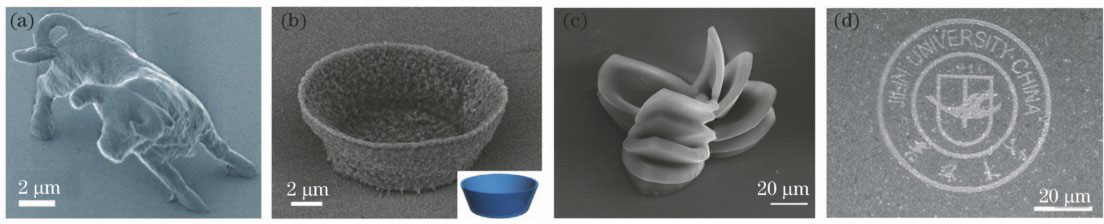
Fig. 2. Schematic of 3D femtosecond laser nanoprinting system
Fig. 3. Micro-nanostructures fabricated via 3D FsLNP. (a) Micro-bull sculpture by raster scanning[23]; (b) micro-basin developed from a bio-photoresist[49]; (c) 3D biomimetic lamellate wrinkle structure developed from a hydrogel[56]; (d) university badge pattern assembled from CdTe quantum dots[57]
Fig. 4. Schematics and SEM images of microlens arrays with different curvature units (MLADC) fabricated via 3D FsLNP. (a) Schematic of perspective view; (b) schematic of cross-section view as well as the focal plane; (c) SEM image shot from top; (d) SEM image shot from side[67]
Fig. 5. Top-view SEM micrographs of the microlasers with different shapes fabricated via 3D FsLNP on the narrow band filter substrate[68]. (a) Circular disk; (b) circular ring; (c) spiral ring; (d) spiral ring stacked on circular ring; (e) spiral ring stacked on circular disk
Fig. 6. 3D FsLNP using diversiform silk-based aqueous inks[49]. (a) Image of silk fibroin extracted from Bombyx mori silkworm cocoons in the inset; (b) image of renewable silk fibroin (RSF) aqueous mother solution (mass fraction of 3%); (c) diversiform silk-based aqueous inks [(I) RSF/MB aqueous solution, (II) RSF/Ag nanoseed aqueous solution, (III) RSF/AgNO3 aqueous solution, (IV) RSF/HAuCl4 aqueous solution]; (d) schematic
Fig. 7. Protein-based multi-mode interference (MMI) optical micro-splitters via 3D FsLNP[88]. (a) Schematic of 3D FsLNP of protein-based MMI micro-splitters; (b) optical microscopic image of protein-based MMI micro-splitters prepared on MgF2 substrate, the scale bar is 10 μm
Fig. 8. Natural compound eye and high quality artificial compound eye via 3D FsLNP combined with the high-speed voxel-modulation laser scanning method[89]. (a) Top-view and(b) magnified SEM images of a natural compound eye showing a macrobase and hundreds of 100% filled hexagonal micro-ommatidia; (c) top-view and (d) 30°-tilted magnified SEM images of the bio-inspired artificial compound eye, the 100% fill factor of hexagonal ommatidia is comparable to t
|
Table 1. Comparison between 3D FsLNP and 3D laser printing

Set citation alerts for the article
Please enter your email address
© Copyright 2018-2021 | Chinese Laser Press. All Rights Reserved 沪ICP备15018463号-20