
Zhiwen Li, Jiangliu Luo, Shengqun Hu, Qiang Liu, Wenjie Yu, Youming Lu, Xinke Liu. Strain enhancement for a MoS2-on-GaN photodetector with an Al2O3 stress liner grown by atomic layer deposition[J]. Photonics Research, 2020, 8(6): 799
- Photonics Research
- Vol. 8, Issue 6, 799 (2020)
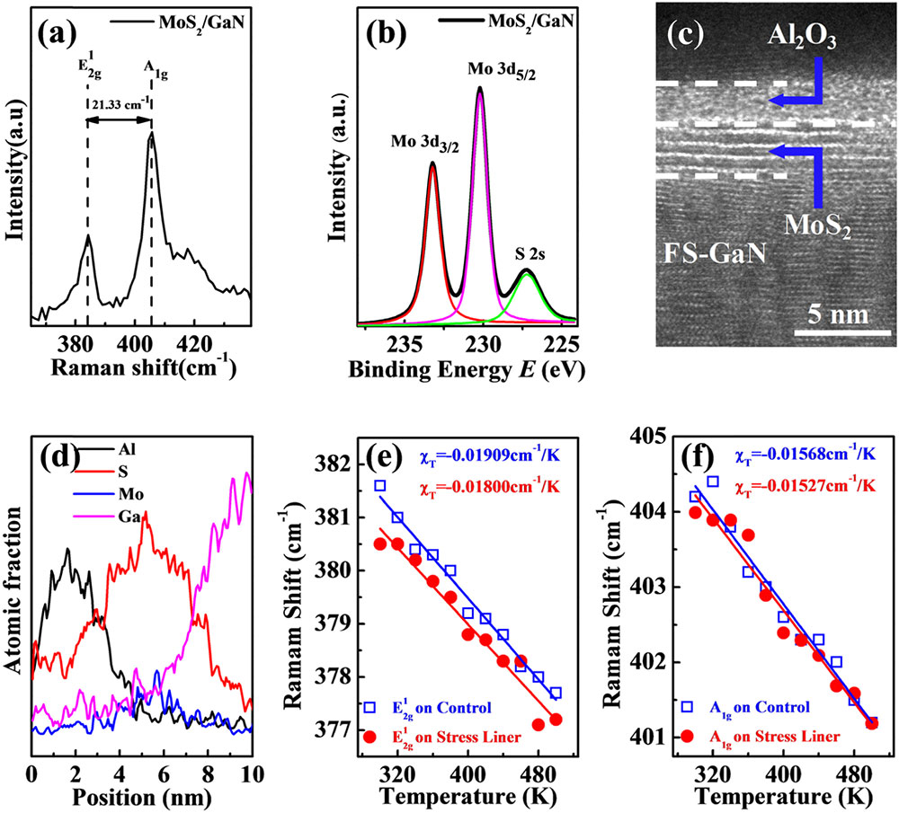
Fig. 1. Material characterization of multilayer MoS 2 Al 2 O 3 MoS 2 E 2 g 1 A 1 g 21.33 cm − 2 MoS 2 / GaN MoS 2 / GaN Al 2 O 3 E 2 g 1 A 1 g
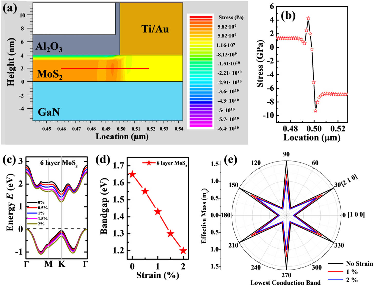
Fig. 2. Simulation of multilayer MoS 2 MoS 2 Al 2 O 3 MoS 2 MoS 2
Fig. 3. Schematic and measurement of MoS 2 Al 2 O 3 MoS 2 Al 2 O 3 I Ph ∝ P α
Fig. 4. Performance of control and stress liner photodetectors. (a) Gain and EQE as a function of incident power; significant increases in both values for stress liner photodetector; (b) NEP and detectivity as a function of incident power; reduced performance of both for stress liner photodetector due to the increase in dark current.
Fig. 5. Time curve of photocurrent with a switch on/off light. (a) Photocurrent-time curve of control and stress liner photodetectors illuminated by 365 nm light source with the incident power of 5.647 μW at 20 V, respectively. The corresponding rise time (from 10% to 90% of maximum photocurrent) and the fall time (from 90% to 10% of maximum photocurrent) of (b) control and (c) stress liner photodetector, respectively.

Set citation alerts for the article
Please enter your email address
© Copyright 2018-2021 | Chinese Laser Press. All Rights Reserved 沪ICP备15018463号-20