Abstract
Strain regulation as an effective way to enhance the photoelectric properties of two-dimensional (2D) transition metal dichalcogenides has been widely employed to improve the performance of photovoltaic devices. In this work, tensile strain was introduced in multilayer grown on GaN by depositing 3 nm of on the surface. The temperature-dependent Raman spectrum shows that the thermal stability of is improved by . Theoretical simulations confirmed the existence of tensile strain on covered with , and the bandgap and electron effective mass of six layers of decreased due to tensile strain, which resulted in an increase of electron mobility. Due to the tensile strain effect, the photodetector with the stress liner achieved better performance under the illumination of 365 nm wavelength, including a higher responsivity of 24.6 A/W, photoconductive gain of 520, and external quantum efficiency of 8381%, which are more than twice the corresponding values of photodetectors without . Our work provides an effective technical way for improving the performance of 2D material photodetectors.1. INTRODUCTION
Two-dimensional (2D) transition metal dichalcogenides (TMDs) have important research value in the fields of optoelectronic devices, energy storage, catalysis, etc., due to their special structure and excellent properties [1–7]. , as a typical representative of TMDs, possesses a bandgap ranging from 1.80 eV (monolayer) to 1.20 eV (bulk), high mobility (), high light absorptivity, and thermal stability (), which facilitate its applications in field effect transistors (FETs), photodetectors, and sensors [8–11]. Furthermore, its excellent mechanical property makes it useful in the application of related flexible and wearable devices. Although the carrier mobility for transistors is estimated to be at room temperature by theoretical calculation [12], the experimental value is normally 1 or 2 orders lower, which significantly limits the performance of the transistors. Then many efforts, e.g., phase engineering [13], dielectric passivation [14], and boron nitride as back-gate dielectric [15], have been implemented to improve performance.
Current research indicates that the properties of 2D TMD materials, such as bandgap [16,17], effective carrier mass [18], conductivity [19], exciton–phonon coupling [20], and spin-orbit coupling [21] can be changed by strain through changing the lattice structure (such as bond length, bond angle, and relative position of atoms) [22] and lattice symmetry [17]. Therefore, the strain regulation of 2D TMDs has aroused great interest from researchers. In the band structure of TMDs, the conduction band mainly comes from the contribution of the orbital of , while the valence band mainly comes from the contribution of the , orbital of and hybridization of , of [23] [here, represents TMDs, is a transition metal element, and is the VI main group element (S, Se, Te)]. When 2D TMDs have in-plane tensile strain, the band structure is changed, which in turn affects the properties of the material due to lattice being stretched, the distance between and being increased, the X−M−X bond angle being decreased, the relative position between the atoms being changed, and the state of the orbital overlap being changed. Li et al. calculated the relationship between the biaxial strain and the absorption spectrum with a strain range of 0%–9%, and found that the excitation energy decreased from 2.0 eV in the unstrained state to 1.1 eV under 9% biaxial strain [24]. It was found using density functional theory (DFT) that as the tensile strain on increases, the bandgap decreases, the conduction band and valence band change due to changes in the lattice constant of the material, and the monolayer changes from a direct bandgap to an indirect bandgap, so strain affects the electron transition process in 2D TMDs [25]. Kis et al. reported that the piezoresistive gauge factor of monolayer is , indicating that the resistance decreases with increasing strain, which can induce the material to change from semiconducting to metallic [26]. Bending, stretching, compressing flexible substrates [18], diamond anvil cell (DAC) [27], and utilizing differences in thermal expansion coefficients of a substrate [28] can be used as ways to induce strain. , which is directly grown on a patterned sapphire substrate (PSS) by chemical vapor deposition (CVD), is subject to compressive strain after rapid temperature drop due to the difference in the thermal expansion coefficient [29]. Strain from mechanical external forces is unstable and uncontrollable and may even damage the integrity of the film. Differences in the lattice constants or thermal expansion coefficients between the substrate and 2D TMDs degrade the quality of grown film. Kufer and Konstantatos reported highly stable and high-performance monolayer and bilayer photodetectors encapsulated by atomic layer-deposited with vanishing hysteresis and reduced device resistance [30]. Even when using scandium contacts on 10-nm thick exfoliated flakes that are covered by a 15 nm film, high effective mobility of is achieved at room temperature [31]. The improvement of the material and device performance induced by the high- dielectric has been primarily attributed to the screening effect on the charged impurity scattering. As a result of first-principles calculation, about 0.41% tensile strain on monolayer can be introduced by 3 nm covering the surface [32]. This implies that high- oxide deposition on 2D TMDs can also introduce strain due to differences in their thermal expansion coefficients. Nevertheless, systematic and insightful studies about the effects of oxide strain layer on 2D TMDs are still essential and important to guide the development of strained TMD devices. It has been reported that the grown on GaN has a shorter effective exciton lifetime, which promotes fast photogenerated electron-hole separation and enables high responsivity and fast response of photodetectors [33–36].
Herein, high quality, large area, and continuous multilayer was successfully grown on a freestanding (FS) GaN substrate (350 μm thick) with (0001) orientation using the CVD method, and a 3 nm thick overlayer was deposited on it by atomic layer deposition (ALD), forming the heterostructure of . Raman spectroscopy, X-ray photoelectron spectroscopy (XPS), and transmission electron microscopy (TEM) characterizations have been carried out to investigate the material. Then -on-GaN photodetectors with and without the stress liner have been fabricated in typical semiconductor fabrication process and fully characterized. After the tensile strain is introduced by the stress liner, the performance of the photodetector, including photocurrent, responsivity, gain, and external quantum efficiency, is significantly improved.
Sign up for Photonics Research TOC. Get the latest issue of Photonics Research delivered right to you!Sign up now
2. METHOD
A. Preparation of the MoS2 on GaN, Al2O3 and Photodetectors
High-quality multilayer is grown by CVD method on a transparent nondoped free-supporting GaN substrate with a size of 1 cm by 1 cm. Before growth, FS GaN substrate (350 μm thick) with (0001) orientation was cleaned with acetone (, 99.5%), isopropanol (, 99.5%), and deionized water in an ultrasonic instrument successively for 10 min, and then dried with high-purity . During the growth process, the S molybdenum trioxide powder (, 99.95%) and sulphur powder as precursors were heated to 250°C and 750°C, respectively, and kept at the temperature for 20 min. Finally, the temperature was naturally decreased to room temperature, and the entire process was continuously passed through Ar with the atmospheric pressure. was deposited on the surfaces of and photodetectors by the ALD method at 250°C, in which precursors are and trimethyl aluminum (TMAl, 99.9999%). The photodetectors were fabricated through a standard photolithography (Suss MA6)-thermal evaporation (ASB-EPI-C6)-lift-off process. Five nm titanium (Ti, 99.999%) and 50 nm gold (Au, 99.999%) were selected as electrode metals to be deposited on the sample surface by the thermal evaporation method, where the role of Ti is to increase the electrode adhesion on .
B. Characterization and Measurement
Room-temperature Raman spectroscopy measurements were carried out in a confocal microscopy setup with a 514 nm solid-state green laser for excitation with the power maintained below 0.25 mW. Temperature-dependent measurements ranging from 300 to 500 K were carried out using a hot plate with adjustable temperature, and samples were allowed for thermal stabilization of 5 min. The XPS was carried out using a VG ESCALAB 220i-XL system with a constant pass energy of 20 eV and a monochromatic Al (1486.6 eV) X-ray source. The core-level binding energy was corrected using C 1s peak at 284.8 eV in order to exclude the sample surface differential charging effect. The lithography process was carried out using a UV contact exposure mask aligner (Munich, MA6) with a power of 365 W. TEM was carried out using an America FEI-Titan Cubed Themis G2 300 with TEM information resolution (nonlinear) of 0.06 nm. The electrical performance characteristics of the related photodetectors were investigated by a Keithley 4200-SCS semiconductor analyzer.
C. Theoretical Simulation
The first-principles calculations involved in this work were performed using the Cambridge Sequential Total Energy Package (CASTEP) based on DFT [33]. Various parameters were set as follows. The maximum Hellmann–Feynman forces was 0.05 eV/Å, the electronic wave functions were expanded in a plane-wave basis set with energy cut-off of 650 eV to ensure convergence, and a Monkhorste-Pack mesh was used in the Brillouin-zone sampling. The total energy changes during the optimization finally converged to less than , the maximum force each atom in the crystal was less than 0.03 eV/nm, the maximum stress in the crystal was less than 0.05 GPa, and the maximum displacement of the atom was less than 0.0001 nm.
3. RESULTS AND DISCUSSION
In order to achieve a high-quality, uniform, and continuous multilayer film, a transparent FS GaN with nearly perfect lattice matching was selected as the deposited substrate in this work. The Raman spectrum at room temperature shown in Fig. 1(a) detected two Raman peaks at and , which are, namely, mode-related to in-plane atom vibration and mode-related to out-of-plane vibration, respectively. The distance between the two peaks was , which indicates that the number of layers of is about five to six layers. Mo (233.44 eV), Mo (230.03 eV), and S 2s (227.57 eV) peaks were exhibited in the XPS spectrum shown in Fig. 1(b), which is consistent with the reported values [34]. In addition, the peak related to Mo–O bonding was not found near 235.7 eV, implying that no byproduct was produced during the growth of . The atomic ratio of S and Mo is about 1.97, which is close to stoichiometric [35,36]. Subsequently, stress liner with 3 nm thickness was deposited on the sample using ALD. Cross-section TEM was carried out on the sample, as shown in Fig. 1(c); the TEM image can be divided into three parts: the thickness of the uppermost part is about 3 nm, the middle part shows a clear layered structure with about 4 nm thickness (corresponding to six layers), and the bottom part has a crystal structure. Combining the distribution curve of atomic fraction with the position shown in Fig. 1(d) by starting straight down along the surface of , these three parts are , , and GaN.
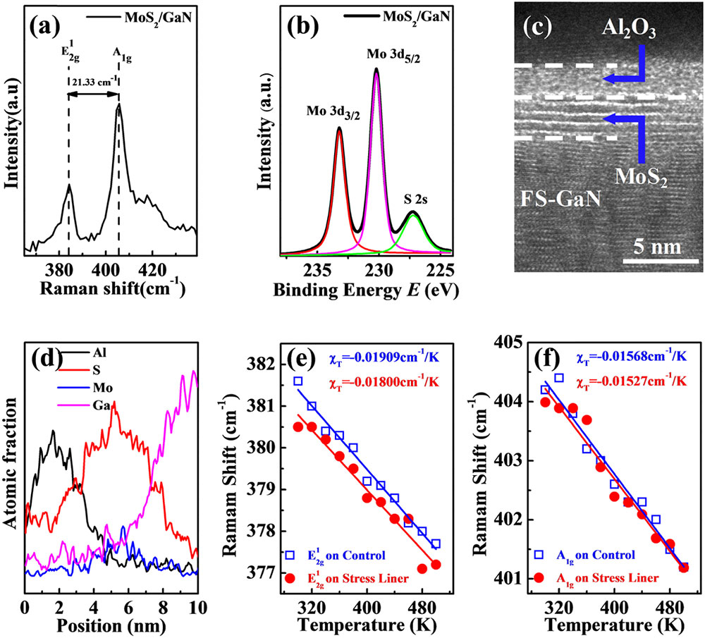
Figure 1.Material characterization of multilayer with and without stress liner. (a) Raman spectra of multilayer sample grown on FS GaN substrate; the distance between and is ; (b) core level XPS spectrum of Mo 3d and S 2s of the control multilayer sample; (c) cross-sectional TEM image of the multilayer with 3 nm ; (d) Al, S, Mo, and Ca element fraction as a function of depth position. The position of Raman mode peaks for (e) and (f) of control and stress liner samples as a function of temperature including a linear fit.
The investigation of temperature-dependent vibrational properties is important for further understanding the electron–phonon interaction, transport properties, and crystal structure of materials, which may largely impact the performance of photoelectronic devices. In this work, temperature-dependent Raman spectra also were determined on the sample (control) and sample (stress liner) to investigate the lattice vibration properties. The Raman spectral curves of control and stress liner samples as a function of temperature variation from 300 to 500 K with a step of 20 K are shown in Figs. S1(a) and S1(b), respectively (see Dataset 1, Ref. [37]). Obvious redshifts of the two peaks in both samples can be observed with the temperature rising, similar to those of the other 2D materials [38–41]. Extracted peak positions of and Raman modes for both samples are shown in Figs. 1(e) and 1(f), respectively. These points can be fitted using this formula [42]: , where is the mode frequency measured at 300 K, is the first-order temperature coefficient, and is the temperature difference relative to 300 K. For the stress liner sample, fitted values of and were about 0.01800 and , respectively, the absolute values of which were smaller than the corresponding values ( and ) of the control sample. Smaller in the former demonstrated a better thermal stability, and these results were consistent with previous reports that an capping layer significantly improves the thermal stability of black phosphorus [43,44]. A possible reason for the improvement of thermal stability is the tensile strain on introduced by , which can soften the phonon vibrations and reduce thermal conductivity of [45].
In order to explore the distribution of the stress after covering 3 nm , the variation of stress on with position was simulated and is shown in the cross-sectional view of Fig. 2(a), which is in the photodetector of the same proportion. The strain in major was calculated to be about 0.58% with a stress of 1.35 GPa using the formula: , where is Young’s modulus taking [46]. under Ti/Au is in a compressed state, and under is in a stretched state. Along the horizontal direction of , the stress as a function of position is shown in Fig. 2(b). There was a maximum of tensile stress near the intersection of the , , and Ti/Au (). The conduction and valence bands of changed due to the introduction of this tensile strain. First-principle calculations based on DFT were used to simulate the band structure of six-layer with and without tensile strain. Figure 2(c) shows the changes at the bottom of the conduction band and the top of valence band with 0%–2% biaxial tensile strain. Unstrained multilayer exhibits an indirect bandgap, and as the strain increases, the conduction band moves downward, the K point of the valence band moves downward, and the bandgap decreases linearly from 1.65 eV without strain to 1.20 eV at 2% biaxial tensile strain, shown in Fig. 2(d), which is similar to the case of a monolayer [24]. Furthermore, the electron effective mass of the lowest conduction band can be estimated by the formula: , where ℏ is the reduced Planck constant. As shown in Fig. 2(e), the electron effective mass of six-layer decreases with increasing biaxial tensile strain, which is related to the enlargement in the degree of bending at the bottom of the conduction band and beneficial in enhancing the electron mobility of .

Figure 2.Simulation of multilayer with tensile strain. (a) 2D stress mapping within the multilayer (4 nm) photodetector with stress liner; (b) horizontal stress distribution within the multilayer layer. Results of first-principles calculations: the variation of (c) the bottom of the conduction band and the top of the valence band, (d) bandgap, and (e) electron effective mass under different tensile strain on six-layer .
A transparent photodetector array with two identical (5 nm) Ti/(50 nm) Au electrodes was fabricated on a sample with a size of 1 cm by 1 cm using a semiconductor processing technology (control photodetector). Figure 3(a) shows a 3D schematic view of the photodetector; about 3 nm was deposited via ALD at the surface of the detector (stress liner photodetector). The photoelectric performance of both photodetectors was fully characterized, and the current (absolute value) curves as a function of voltage (from to 20 V) under dark and 365 nm light with different powers are exhibited in Fig. 3(b). For the control device, the dark current was about 94.6 nA at 20 V, indicating the multilayer grown on GaN was undoped, and the Fermi level resided in the bandgap [47]. At the same voltage, the 365 nm laser irradiation with 5.647 μW power made the current increase by 3 orders of magnitude due to the generation of photocarriers in the material, which is considered as optical doping [48]. For the stress liner photodetector, a significant increase in dark current can be observed after stress liner, which is due to reduced bandgap under tensile strain.
Figure 3.Schematic and measurement of photodetector with and without stress liner. (a) 3D schematic structure view of multilayer photodetectors with the stress liner; (b) dark current and light current as a function of voltage under different power of the 365 nm incident light for control and stress liner photodetector; (c) extracted photocurrent of two photodetectors at 20 V with varying incident power. The straight lines were fitted by the power law (). (d) Calculated responsitivity of two photodetectors as a function of incident power.
Similarly, the current was also greatly increased by the generation of photocarriers under different powers of illumination for the stress liner photodetector. Photocurrent can be extracted by the equation: , where and are the current in dark condition and under illumination, respectively. Figure 3(c) shows the scattered point distribution of the photocurrent under different incident powers with 365 nm wavelength at 20 V voltage, and more than twice the increase of the photocurrent could be observed in the stress liner photodetector due to tensile strain in comparison with the control photodetector. For both photodetectors, linear increases of photocurrent with incident power could be fitted using the power law . The values of decreased from 1.22 of control to 0.99 of the stress liner photodetector, implying routes of the loss of the photoexcited carrier by a recombination existed [49,50], and both the defects of the and the charge impurities around the could be recombination centers. Similar behavior exists in other nanomaterials reported, such as monolayer [51,52], Si [53], ZnO [49], and GaN nanowires [50]. Responsitivity is a measure of the photoelectric conversion characteristics of a photodetector and the spectral and frequency characteristics of the photoelectric conversion, which was calculated by using the equation: , where is the power of the incident light irradiated to the active part of the photodetector, which is normalized by the equation: , where is the output power of the laser source. The calculated values of control and stress liner photodetectors are plotted as a function of laser incident power under a bias voltage of 20 V in Fig. 3(d). The responsivity values of the control photodetector showed a trend of rising as the irradiation power increased and then decreased, and the achieved maximum was about 11.30 A/W at , which is because carrier lifetime increases resulting in the carrier recombination became less frequent at low excitation power [54], which is ascribed to the reduced carrier recombination rate. Due to tensile strain effect, the extracted highest achievable responsivity value in stress liner photodetector was 24.62 A/W at , which is more than twice the corresponding value of the control photodetector. Due to the high quality of the multilayer grown in this work, the photocurrent and responsivity are higher than that of the previously reported monolayer photodetectors [5,7,8]. The enhancement in photocurrent and in responsivity indicates that tensile strain effectively improves the performances of the photodetector, which is consistent with the results reported by Kuo et al. [29].
To further evaluate the performance of both photodetectors, photoconductive gain and external quantum efficiency (EQE) were also estimated and are shown in Fig. 4(a). Photoconductive gain , representing the number of carriers in the photocurrent, can be generated by one absorbed photon, and is estimated by the equation: , where is incident power, is the frequency of the incident laser, is the Planck constant, is the elementary charge, and is the absorbed power defined as . In order to acquire the absorption percentage , the absorbance curves of the sample were also measured in this work, which were obtained by subtracting the absorbance of the blank GaN substrate and plotting it as a function of the incident wavelength shown in Fig. S2 (see Dataset 1, Ref. [37]). Due to the “absorbance ,” which is defined as , where and are the intensity of incident light and transmitted light, respectively, the absorption percentage can be obtained by . When the wavelength is 365 nm, is about 16.13% using . The maximum value of photoconductive gain in the stress liner photodetector is 520, which is much bigger than the corresponding maximum value 239 of the control photodetector, demonstrating that with an stress liner can generate more carriers contributing to the photocurrent due to tensile strain effect. EQE refers to the average number of electrons released in the photodetector resulting from each incident photon. It is related to the energy of the incident laser, and expressed by . Similarly, the highest values of the extracted EQE are 3848% for the control photodetector and 8381% for the stress liner photodetector. Such a significant increase in EQE illustrates that tensile strain can increase the number of electrons generated per incident photon per unit time.
Figure 4.Performance of control and stress liner photodetectors. (a) Gain and EQE as a function of incident power; significant increases in both values for stress liner photodetector; (b) NEP and detectivity as a function of incident power; reduced performance of both for stress liner photodetector due to the increase in dark current.
Noise equivalent power (NEP) and normalized detectivity () are parameters that describe the detection capability of a photodetector. Lower NEP and higher indicate a better detection capability of photodetectors. NEP and are estimated by the equations: and , respectively, where is the current in the dark state and is the bandwidth. Herein, we use , and the active area of the device refers to the part where the two electrodes face each other and is calculated as . As the Fig. 4(b) shows, NEP increases and decreases can be observed in the photodetector with the stress liner. Compared to the multilayer photodetector grown on sapphire, the photodetector has better detection capabilities due to the near-perfect lattice matching [6]. The reduction of the detection capability can mainly be attributed to the enlargement of the bandgap of , the increase of the carrier concentration, and the dark current of the photodetector under the effect of tensile strain.
Finally, the time-response behavior for both photodetectors was measured using a 365 nm light at a power of 5.642 μW, alternately switched on/off every 10 s. The photocurrent for two photodetectors as a function of time under a fixed voltage 20 V is shown in Fig. 5(a). A repeatable and stable photo-switching behavior is observed. In addition, the corresponding rise time, taken from 10% to 90% of maximum photocurrent, and the fall time, taken from 90% to 10% of maximum photocurrent, are shown in Figs. 5(b) and 5(c), respectively, which were obtained by selecting and zooming in on one of the cycles in the curves. In comparison, the rise time was reduced from 21.1 s of the control photodetector to 12.8 s of the stress liner photodetector, and the corresponding fall time was increased from 19.7 to 26.4 s. The shortening current rise time is mainly due to the increased electron mobility induced by decreased electron effective mass of under tensile strain effect, and the extended current fall time is mainly owing to the carriers being captured by the defects existing in .
Figure 5.Time curve of photocurrent with a switch on/off light. (a) Photocurrent-time curve of control and stress liner photodetectors illuminated by 365 nm light source with the incident power of 5.647 μW at 20 V, respectively. The corresponding rise time (from 10% to 90% of maximum photocurrent) and the fall time (from 90% to 10% of maximum photocurrent) of (b) control and (c) stress liner photodetector, respectively.
4. CONCLUSION
High-quality continuous multilayer was prepared on an FS GaN substrate using CVD and characterized by Raman spectroscopy and XPS. ALD was used to deposit 3 nm on a sample. Temperature-dependent Raman spectroscopy was carried out to demonstrate that the thermal stability of was improved due to the tensile strain effect inducted by . The theoretical simulation shows that the multilayer with 3 nm stress liner is stretched, which results in reduction of the bandgap and electron effective mass. Under illumination of 365 nm, a state-of-the-art performance was demonstrated in the stress liner photodetector, leading to a responsivity of 24.6 A/W, a gain of 520, and an EQE of 8381%. These are more than twice the corresponding values of the control photodetector. The shortened current rise time under illumination is due to improved electron mobility by introducing tensile strain. This work demonstrates an effective method to improve the performance of 2D material photodetectors and may guide the development of next-generation imaging systems.
Acknowledgment
Acknowledgment. The authors wish to acknowledge the assistance on HRTEM observation received from the Electron Microscope Center of the Shenzhen University, and device fabrication process in the Photonics Center of Shenzhen University.
References
[1] Y. Xiao, M. Zhou, J. Liu, J. Xu, L. Fu. Phase engineering of two-dimensional transition metal dichalcogenides. Sci. China Mater., 62, 759-775(2019).
[2] M. Ju, X. Liang, J. Liu, L. Zhou, Z. Liu, R. G. Mendes, M. H. Rümmeli, L. Fu. Universal substrate-trapping strategy to grow strictly monolayer transition metal dichalcogenides crystals. Chem. Mater., 29, 6095-6103(2017).
[3] Q. Zhang, L. Fu. Novel insights and perspectives into weakly coupled ReS2 toward emerging applications. Chem, 5, 505-525(2019).
[4] Q. Zhang, Y. Xiao, T. Zhang, Z. Weng, M. Zeng, S. Yue, R. G. Mendes, L. Wang, S. Chen, M. H. Rümmeli, L. Peng, L. Fu. Iodine-mediated chemical vapor deposition growth of metastable transition metal dichalcogenides. Chem. Mater., 29, 4641-4644(2017).
[5] Z. Li, J. Wu, C. Wang, H. Zhang, W. Yu, Y. Lu, X. Liu. High-performance monolayer MoS2 photodetector enabled by oxide stress liner using scalable chemical vapor growth method. Nanophotonics(2020).
[6] A. Sourav, Z. Li, Z. Huang, V. D. Botcha, C. Hu, J.-P. Ao, Y. Peng, H.-C. Kuo, J. Wu, X. Liu, K.-W. Ang. Large-scale transparent molybdenum disulfide plasmonic photodetector using split bull eye structure. Adv. Opt. Mater., 6, 1800461(2018).
[7] X. Huang, X. Feng, L. Chen, L. Wang, W. C. Tan, L. Huang, K.-W. Ang. Fabry-Perot cavity enhanced light-matter interactions in two-dimensional van der Waals heterostructure. Nano Energy, 62, 667-673(2019).
[8] B. Radisavljevic, A. Radenovic, J. Brivio, V. Giacometti, A. Kis. Single-layer MoS2 transistors. Nat. Nanotechnol., 6, 147-150(2011).
[9] S. Kim, A. Konar, W.-S. Hwang, J. H. Lee, J. Lee, J. Yang, C. Jung, H. Kim, J.-B. Yoo, J.-Y. Choi, Y. W. Jin, S. Y. Lee, D. Jena, W. Choi, K. Kim. High-mobility and low-power thin-film transistors based on multilayer MoS2 crystals. Nat. Commun., 3, 1011(2012).
[10] T. Wang, R. Zhu, J. Zhuo, Z. Zhu, Y. Shao, M. Li. Direct detection of DNA below ppb level based on thionin-functionalized layered MoS2 electrochemical sensors. Anal. Chem., 86, 12064-12069(2014).
[11] Z. P. Ling, R. Yang, J. W. Chai, S. J. Wang, W. S. Leong, Y. Tong, D. Lei, Q. Zhou, X. Gong, D. Z. Chi, K. W. Ang. Large-scale two-dimensional MoS2 photodetectors by magnetron sputtering. Opt. Express, 23, 13580-13586(2015).
[12] F. Liu, Y. Wang, X. Liu, J. Wang, H. Guo. A theoretical investigation of orientation-dependent transport in monolayer MoS2 transistors at the ballistic limit. IEEE Electron Device Lett., 36, 1091-1093(2015).
[13] R. Kappera, D. Voiry, S. E. Yalcin, B. Branch, G. Gupta, A. D. Mohite, M. Chhowalla. Phase-engineered low-resistance contacts for ultrathin MoS2 transistors. Nat. Mater., 13, 1128-1134(2014).
[14] J.-G. Song, S. J. Kim, W. J. Woo, Y. Kim, I.-K. Oh, G. H. Ryu, Z. Lee, J. H. Lim, J. Park, H. Kim. Effect of Al2O3 deposition on performance of top-gated monolayer MoS2-based field effect transistor. ACS Appl. Mater. Interfaces, 8, 28130-28135(2016).
[15] Q. A. Vu, S. Fan, S. H. Lee, M.-K. Joo, W. J. Yu, Y. H. Lee. Near-zero hysteresis and near-ideal subthreshold swing in h-BN encapsulated single-layer MoS2 field-effect transistors. 2D Mater., 5, 031001(2018).
[16] M. Zeng, Y. Xiao, J. Liu, K. Yang, L. Fu. Exploring two-dimensional materials toward the next-generation circuits: from monomer design to assembly control. Chem. Rev., 118, 6236-6296(2018).
[17] S. Manzeli, D. Ovchinnikov, D. Pasquier, O. V. Yazyev, A. Kis. 2D transition metal dichalcogenides. Nat. Rev. Mater., 2, 17033(2017).
[18] H. J. Conley, B. Wang, J. I. Ziegler, R. F. Haglund, S. T. Pantelides, K. I. Bolotin. Bandgap engineering of strained monolayer and bilayer MoS2. Nano Lett., 13, 3626-3630(2013).
[19] J. Qi, Y.-W. Lan, A. Z. Stieg, J.-H. Chen, Y.-L. Zhong, L.-J. Li, C.-D. Chen, Y. Zhang, K. L. Wang. Piezoelectric effect in chemical vapour deposition-grown atomic-monolayer triangular molybdenum disulfide piezotronics. Nat. Commun., 6, 7430(2015).
[20] I. Niehues, R. Schmidt, M. Drüppel, P. Marauhn, D. Christiansen, M. Selig, G. Berghäuser, D. Wigger, R. Schneider, L. Braasch, R. Koch, A. Castellanos-Gomez, T. Kuhn, A. Knorr, E. Malic, M. Rohlfing, S. Michaelis de Vasconcellos, R. Bratschitsch. Strain control of exciton-phonon coupling in atomically thin semiconductors. Nano Lett., 18, 1751-1757(2018).
[21] X. Dou, K. Ding, D. Jiang, X. Fan, B. Sun. Probing spin-orbit coupling and interlayer coupling in atomically thin molybdenum disulfide using hydrostatic pressure. ACS Nano, 10, 1619-1624(2016).
[22] S. Deng, A. V. Sumant, V. Berry. Strain engineering in two-dimensional nanomaterials beyond graphene. Nano Today, 22, 14-35(2018).
[23] R. Roldán, A. Castellanos-Gomez, E. Cappelluti, F. Guinea. Strain engineering in semiconducting two-dimensional crystals. J. Phys. Condens. Matter., 27, 313201(2015).
[24] J. Feng, X. Qian, C.-W. Huang, J. Li. Strain-engineered artificial atom as a broad-spectrum solar energy funnel. Nat. Photonics, 6, 866-872(2012).
[25] S. Pak, J. Lee, Y.-W. Lee, A. R. Jang, S. Ahn, K. Y. Ma, Y. Cho, J. Hong, S. Lee, H. Y. Jeong, H. Im, H. S. Shin, S. M. Morris, S. Cha, J. I. Sohn, J. M. Kim. Strain-mediated interlayer coupling effects on the excitonic behaviors in an epitaxially grown MoS2/WS2 van der Waals heterobilayer. Nano Lett., 17, 5634-5640(2017).
[26] S. Manzeli, A. Allain, A. Ghadimi, A. Kis. Piezoresistivity and strain-induced band gap tuning in atomically thin MoS2. Nano Lett., 15, 5330-5335(2015).
[27] A. P. Nayak, S. Bhattacharyya, J. Zhu, J. Liu, X. Wu, T. Pandey, C. Jin, A. K. Singh, D. Akinwande, J.-F. Lin. Pressure-induced semiconducting to metallic transition in multilayered molybdenum disulphide. Nat. Commun., 5, 3731(2014).
[28] G. H. Ahn, M. Amani, H. Rasool, D.-H. Lien, J. P. Mastandrea, J. W. Ager, M. Dubey, D. C. Chrzan, A. M. Minor, A. Javey. Strain-engineered growth of two-dimensional materials. Nat. Commun., 8, 608(2017).
[29] S.-W. Wang, H. Medina, K.-B. Hong, C.-C. Wu, Y. Qu, A. Manikandan, T.-Y. Su, P.-T. Lee, Z.-Q. Huang, Z. Wang, F.-C. Chuang, H.-C. Kuo, Y.-L. Chueh. Thermally strained band gap engineering of transition-metal dichalcogenide bilayers with enhanced light-matter interaction toward excellent photodetectors. ACS Nano, 11, 8768-8776(2017).
[30] D. Kufer, G. Konstantatos. Highly sensitive, encapsulated MoS2 photodetector with gate controllable gain and speed. Nano Lett., 15, 7307-7313(2015).
[31] S. Das, H.-Y. Chen, A. V. Penumatcha, J. Appenzeller. High performance multilayer MoS2 transistors with scandium contacts. Nano Lett., 13, 100-105(2013).
[32] S. Yu, S. Ran, H. Zhu, K. Eshun, C. Shi, K. Jiang, K. Gu, F. J. Seo, Q. Li. Study of interfacial strain at the α-Al2O3/monolayer MoS2 interface by first principle calculations. Appl. Surf. Sci., 428, 593-597(2018).
[33] M. D. Segall, P. J. D. Lindan, M. J. Probert, C. J. Pickard, P. J. Hasnip, S. J. Clark, M. C. Payne. First-principles simulation: ideas, illustrations and the CASTEP code. J. Phys. Condens. Matter, 14, 2717-2744(2002).
[34] M. A. Baker, R. Gilmore, C. Lenardi, W. Gissler. XPS investigation of preferential sputtering of S from MoS2 and determination of MoSx stoichiometry from Mo and S peak positions. Appl. Surf. Sci., 150, 255-262(1999).
[35] J. Kong, K. T. Park, A. C. Miller, K. Klier. Molybdenum disulfide single crystal (0002) plane XPS spectra. Surf. Sci. Spectra, 7, 69-74(2000).
[36] D. Ruzmetov, K. Zhang, G. Stan, B. Kalanyan, G. R. Bhimanapati, S. M. Eichfeld, R. A. Burke, P. B. Shah, T. P. O’Regan, F. J. Crowne, A. G. Birdwell, J. A. Robinson, A. V. Davydov, T. G. Ivanov. Vertical 2D/3D semiconductor heterostructures based on epitaxial molybdenum disulfide and gallium nitride. ACS Nano, 10, 3580-3588(2016).
[37] Raman and Absorbance of multilayer MoS2. Dataset 1.
[38] I. Calizo, A. A. Balandin, W. Bao, F. Miao, C. N. Lau. Temperature dependence of the Raman spectra of graphene and graphene multilayers. Nano Lett., 7, 2645-2649(2007).
[39] L. Su, Y. Zhang, Y. Yu, L. Cao. Dependence of coupling of quasi 2-D MoS2 with substrates on substrate types, probed by temperature dependent Raman scattering. Nanoscale, 6, 4920-4927(2014).
[40] S. Lei, L. Ge, S. Najmaei, A. George, R. Kappera, J. Lou, M. Chhowalla, H. Yamaguchi, G. Gupta, R. Vajtai, A. D. Mohite, P. M. Ajayan. Evolution of the electronic band structure and efficient photo-detection in atomic layers of InSe. ACS Nano, 8, 1263-1272(2014).
[41] D. J. Late. Temperature dependent phonon shifts in few-layer black phosphorus. ACS Appl. Mater. Interfaces, 7, 5857-5862(2015).
[42] A. S. Pawbake, M. S. Pawar, S. R. Jadkar, D. J. Late. Large area chemical vapor deposition of monolayer transition metal dichalcogenides and their temperature dependent Raman spectroscopy studies. Nanoscale, 8, 3008-3018(2016).
[43] S. X. Yang, C. Wang, C. Ataca, Y. Li, H. Chen, H. Cai, A. Suslu, J. C. Grossman, C. B. Jiang, Q. Liu, S. Tongay. Self-driven photodetector and ambipolar transistor in atomically thin GaTe-MoS2 p–n vdW heterostructure. ACS Appl. Mater. Interfaces, 8, 2533-2539(2016).
[44] X. Feng, V. V. Kulish, P. Wu, X. Liu, K.-W. Ang. Anomalously enhanced thermal stability of phosphorene via metal adatom doping: an experimental and first-principles study. Nano Res., 9, 2687-2695(2016).
[45] Z. Ding, Q.-X. Pei, J.-W. Jiang, Y.-W. Zhang. Manipulating the thermal conductivity of monolayer MoS2 via lattice defect and strain engineering. J. Phys. Chem. C, 119, 16358-16365(2015).
[46] S. Bertolazzi, J. Brivio, A. Kis. Stretching and breaking of ultrathin MoS2. ACS Nano, 5, 9703-9709(2011).
[47] A. R. Klots, A. K. M. Newaz, B. Wang, D. Prasai, H. Krzyzanowska, J. Lin, D. Caudel, N. J. Ghimire, J. Yan, B. L. Ivanov, K. A. Velizhanin, A. Burger, D. G. Mandrus, N. H. Tolk, S. T. Pantelides, K. I. Bolotin. Probing excitonic states in suspended two-dimensional semiconductors by photocurrent spectroscopy. Sci. Rep., 4, 6608(2014).
[48] H. S. Lee, M. S. Kim, H. Kim, Y. H. Lee. Identifying multiexcitons in MoS2 monolayers at room temperature. Phys. Rev. B, 93, 140409(2016).
[49] C. Soci, A. Zhang, B. Xiang, S. A. Dayeh, D. P. R. Aplin, J. Park, X. Y. Bao, Y. H. Lo, D. Wang. ZnO nanowire UV photodetectors with high internal gain. Nano Lett., 7, 1003-1009(2007).
[50] F. González-Posada, R. Songmuang, M. Den Hertog, E. Monroy. Room-temperature photodetection dynamics of single GaN nanowires. Nano Lett., 12, 172-176(2012).
[51] W. Zhang, J.-K. Huang, C.-H. Chen, Y.-H. Chang, Y.-J. Cheng, L.-J. Li. High-gain phototransistors based on a CVD MoS2 monolayer. Adv. Mater., 25, 3456-3461(2013).
[52] A. E. Yore, K. K. H. Smithe, S. Jha, K. Ray, E. Pop, A. K. M. Newaz. Large array fabrication of high performance monolayer MoS2 photodetectors. Appl. Phys. Lett., 111, 043110(2017).
[53] A. Zhang, S. You, C. Soci, Y. Liu, D. Wang, Y.-H. Lo. Silicon nanowire detectors showing phototransistive gain. Appl. Phys. Lett., 93, 121110(2008).
[54] L. Huang, W. C. Tan, L. Wang, B. Dong, C. Lee, K.-W. Ang. Infrared black phosphorus phototransistor with tunable responsivity and low noise equivalent power. ACS Appl. Mater. Interfaces, 9, 36130-36136(2017).


