• Laser & Optoelectronics Progress
  • Vol. 58, Issue 10, 1011002 (2021)
Lingdong Kong1、2、†, Qingyuan Zhao1、2、*†, Xuecou Tu1、2, Labao Zhang1、2, Xiaoqing Jia1、2, Lin Kang1、2, Jian Chen1、2, and Peiheng Wu1、2
Author Affiliations
  • 1School of Electronic Science and Engineering, Nanjing University, Nanjing, Jiangsu 210023, China
  • 2Research Institute of Superconductor Electronics, Nanjing University, Nanjing, Jiangsu 210023, China
  • show less
    DOI: 10.3788/LOP202158.1011002 Cite this Article Set citation alerts
    Lingdong Kong, Qingyuan Zhao, Xuecou Tu, Labao Zhang, Xiaoqing Jia, Lin Kang, Jian Chen, Peiheng Wu. Progress and Applications of Superconducting Nanowire Delay-Line Single-Photon Imagers[J]. Laser & Optoelectronics Progress, 2021, 58(10): 1011002 Copy Citation Text show less
    Superconducting nanowire single-photon detector (SNSPD). (a) Typical meandered nanowire; (b) equivalent circuit of SNSPD; (c) waveform of output pulse
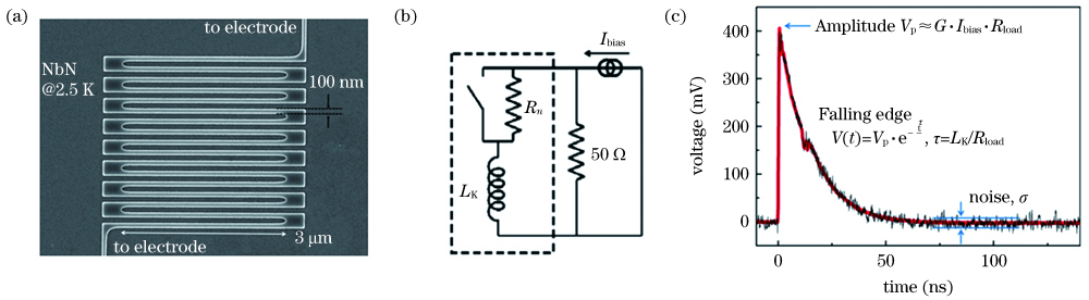
    Fig. 1. Superconducting nanowire single-photon detector (SNSPD). (a) Typical meandered nanowire; (b) equivalent circuit of SNSPD; (c) waveform of output pulse
    Schematic of reading the spatial and temporal information of a photon in a superconducting nanowire delay line
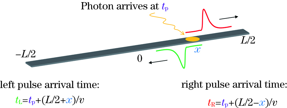
    Fig. 2. Schematic of reading the spatial and temporal information of a photon in a superconducting nanowire delay line
    Microwave characteristics of a superconducting nanowire. (a) Characteristic impedance and velocity of superconducting coplanar waveguides (The superconducting film is NbN with a kinetic inductance of 80 pH/square. The substrate is thermal dioxide silicon. The gap between signal line and ground is fixed at 500 nm.); (b) characteristic impedance and velocity of coplanar waveguides made from normal metal (no kinetic inductance); (c) ratio of kinetic inductance to geometric inductance
    Fig. 3. Microwave characteristics of a superconducting nanowire. (a) Characteristic impedance and velocity of superconducting coplanar waveguides (The superconducting film is NbN with a kinetic inductance of 80 pH/square. The substrate is thermal dioxide silicon. The gap between signal line and ground is fixed at 500 nm.); (b) characteristic impedance and velocity of coplanar waveguides made from normal metal (no kinetic inductance); (c) ratio of kinetic inductance to geometric inductance
    Different geometries of superconducting nanowire delay line imagers. (a) A single nanowires both acts as a detector and a delay line[20]; (b) detectors and delay lines are separated to build a two-dimensional array, and the delay lines are made from wide nanowires while detectors are made from 3-SNAPs[21]; (c) simulated current distribution in a 3-SNAP; (d) detectors and delay lines are separated to build a linear array
    Fig. 4. Different geometries of superconducting nanowire delay line imagers. (a) A single nanowires both acts as a detector and a delay line[20]; (b) detectors and delay lines are separated to build a two-dimensional array, and the delay lines are made from wide nanowires while detectors are made from 3-SNAPs[21]; (c) simulated current distribution in a 3-SNAP; (d) detectors and delay lines are separated to build a linear array
    Schematic of the readout circuit for a SNSPI
    Fig. 5. Schematic of the readout circuit for a SNSPI
    Characteristics of the spatial and temporal detections with a SNSPI[21]. (a) Waveforms of output pulses from the two terminals; (b) 1D histogram of the differential times; (c) enlarged view of the 1D histogram; (d) 2D map of the normalized photon counts; (e) histogram of the normalized photon counts for all 256 pixels; (f) histogram of the photon arrival times (The timing jitter is defined as the FWHM of the histogram, which is 60 ps)
    Fig. 6. Characteristics of the spatial and temporal detections with a SNSPI[21]. (a) Waveforms of output pulses from the two terminals; (b) 1D histogram of the differential times; (c) enlarged view of the 1D histogram; (d) 2D map of the normalized photon counts; (e) histogram of the normalized photon counts for all 256 pixels; (f) histogram of the photon arrival times (The timing jitter is defined as the FWHM of the histogram, which is 60 ps)
    Single-photon imaging system[21]. (a) Photo of the imaging setup; (b) schematic of the imaging system
    Fig. 7. Single-photon imaging system[21]. (a) Photo of the imaging setup; (b) schematic of the imaging system
    Block diagram of the algorithmicprocess[21]
    Fig. 8. Block diagram of the algorithmicprocess[21]
    Comparison of the 3D slicing denoising algorithm with the other methods[21]
    Fig. 9. Comparison of the 3D slicing denoising algorithm with the other methods[21]
    Imaging results at different background levels
    Fig. 10. Imaging results at different background levels
    Simulation of the denoising performance at different timing jitters[21]. (a) Average width of all pixelwise gates versus the timing jitter; (b) remaining signal photon number and noise photon number per pixel on average versus the timing jitter; (c) signal-to-noise selectivity ratio versus the timing jitter
    Fig. 11. Simulation of the denoising performance at different timing jitters[21]. (a) Average width of all pixelwise gates versus the timing jitter; (b) remaining signal photon number and noise photon number per pixel on average versus the timing jitter; (c) signal-to-noise selectivity ratio versus the timing jitter
    Lingdong Kong, Qingyuan Zhao, Xuecou Tu, Labao Zhang, Xiaoqing Jia, Lin Kang, Jian Chen, Peiheng Wu. Progress and Applications of Superconducting Nanowire Delay-Line Single-Photon Imagers[J]. Laser & Optoelectronics Progress, 2021, 58(10): 1011002
    Download Citation