• Optoelectronic Technology
  • Vol. 43, Issue 2, 91 (2023)
Jia ZHOU, Jinjian YAN, Zhiqiang LIU, Ying JIANG, Yang HUANG Kai BAO, Jinchai LI, and Deyun ZHOU
Author Affiliations
  • School of Microelectronics, Northwestern Polytechnical University, Xi'an 7092, CHN
  • show less
    DOI: 10.19453/j.cnki.1005-488x.2023.02.001 Cite this Article
    Jia ZHOU, Jinjian YAN, Zhiqiang LIU, Ying JIANG, Yang HUANG Kai BAO, Jinchai LI, Deyun ZHOU. The Current Bottleneck and Technical Progress of Micro LED[J]. Optoelectronic Technology, 2023, 43(2): 91 Copy Citation Text show less
    The overview and advantages of Micro LED
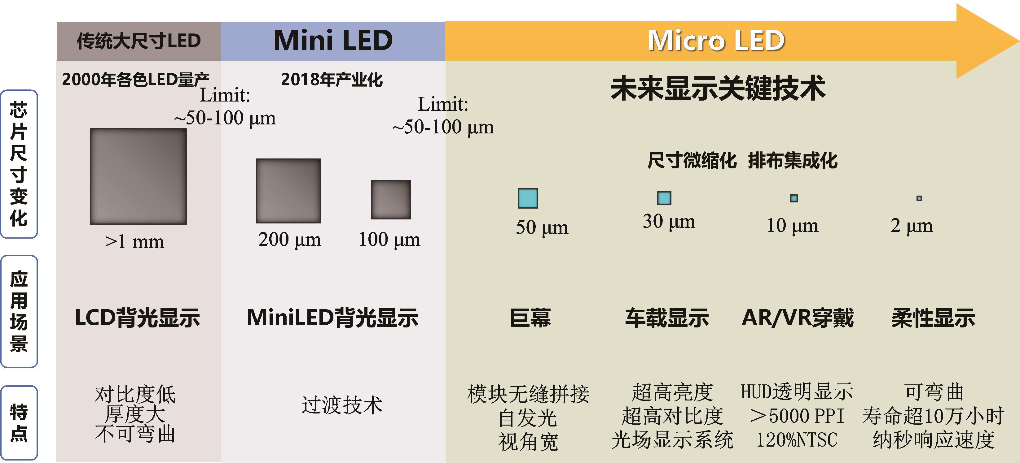
    Fig. 1. The overview and advantages of Micro LED
    [in Chinese]
    Fig. 1. [in Chinese]
    Luminous structure of LCD, OLED and Micro LED display screens
    Fig. 2. Luminous structure of LCD, OLED and Micro LED display screens
    Comparison of LCD and Micro LED display screens
    Fig. 3. Comparison of LCD and Micro LED display screens
    Comparison of LCD, OLED, and Micro LED display technology performance[6-10]
    Fig. 4. Comparison of LCD, OLED, and Micro LED display technology performance[6-10]
    Main process flow of Micro LED manufacturing
    Fig. 5. Main process flow of Micro LED manufacturing
    Typical efficiency curves and structure of nitride LEDs[14]
    Fig. 6. Typical efficiency curves and structure of nitride LEDs[14]
    Number of quantum wells and carrier matching under low current density [17]
    Fig. 7. Number of quantum wells and carrier matching under low current density [17]
    The ratio of the comprehensive SRH recombination rate and comprehensive radiation recombination rate of Micro LEDs A, B, and C, and the illustrations (a), (b), and (c) show the profiles of the SRH recombination rate and radiation recombination rate of Micro LEDs A, B, and C at the edge of the countertop, respectively [18]
    Fig. 8. The ratio of the comprehensive SRH recombination rate and comprehensive radiation recombination rate of Micro LEDs A, B, and C, and the illustrations (a), (b), and (c) show the profiles of the SRH recombination rate and radiation recombination rate of Micro LEDs A, B, and C at the edge of the countertop, respectively [18]
    Effect of EBL on Micro LED performance under low current density[17]
    Fig. 9. Effect of EBL on Micro LED performance under low current density[17]
    Comparison between RGB chip size reduction and quantum efficiency reduction
    Fig. 10. Comparison between RGB chip size reduction and quantum efficiency reduction
    Schematic diagram of the relationship between LED current components and internal quantum efficiency
    Fig. 11. Schematic diagram of the relationship between LED current components and internal quantum efficiency
    Improvement of edge damage areas before and after wet etching
    Fig. 12. Improvement of edge damage areas before and after wet etching
    Schematic diagram of ALD-AlN passivation layer structure and side wall deposition insulation passivation layer [33]
    Fig. 13. Schematic diagram of ALD-AlN passivation layer structure and side wall deposition insulation passivation layer [33]
    Structure diagram and performance improvement of Micro LED with ALD passivation layer [35]
    Fig. 14. Structure diagram and performance improvement of Micro LED with ALD passivation layer [35]
    Schematic diagram and scanning electron microscope image of Micro LED with sol-gel SiO2 passivation, with the illustration showing the schematic diagram of the sol-gel reaction on GaN LED nanorods [37]
    Fig. 15. Schematic diagram and scanning electron microscope image of Micro LED with sol-gel SiO2 passivation, with the illustration showing the schematic diagram of the sol-gel reaction on GaN LED nanorods [37]
    Luminous images and electrical properties of nanorod LEDs with different surface passivation methods[37]
    Fig. 16. Luminous images and electrical properties of nanorod LEDs with different surface passivation methods[37]
    Device structure and photoluminescence (PL) spectrum of Micro LED[40]
    Fig. 17. Device structure and photoluminescence (PL) spectrum of Micro LED[40]
    Optical performance characterization of Micro LED with different repair schemes[40]
    Fig. 18. Optical performance characterization of Micro LED with different repair schemes[40]
    Schematic diagram of selected region growth and cross-sectional SEM image[41]
    Fig. 19. Schematic diagram of selected region growth and cross-sectional SEM image[41]
    The emission image of the Micro LED device array and the SEM image of the epitaxial wafer of the Micro LED array, with a device diameter of 2 μm and a spacing of 1.5 μm[42]
    Fig. 20. The emission image of the Micro LED device array and the SEM image of the epitaxial wafer of the Micro LED array, with a device diameter of 2 μm and a spacing of 1.5 μm[42]
    Schematic diagram of InGaN LED sub micron level pixelization achieved through mesa etching and TIIP[43]
    Fig. 21. Schematic diagram of InGaN LED sub micron level pixelization achieved through mesa etching and TIIP[43]
    TIIP pixelated display array PL images and optoelectronic performance[43]
    Fig. 22. TIIP pixelated display array PL images and optoelectronic performance[43]
    Schematic diagram, electrical performance, and EL emission image of Micro LED treated with p-GaN passivation[44]
    Fig. 23. Schematic diagram, electrical performance, and EL emission image of Micro LED treated with p-GaN passivation[44]
    Current hole structure, Micro LED device structure, PL image, and maximum current density[46]
    Fig. 24. Current hole structure, Micro LED device structure, PL image, and maximum current density[46]
    Schematic diagram of reference device and improved device, with the illustration showing the EL image of the improved device at 8 V voltage[47]
    Fig. 25. Schematic diagram of reference device and improved device, with the illustration showing the EL image of the improved device at 8 V voltage[47]
    Schematic diagram of optical lens synthesis method[48]
    Fig. 26. Schematic diagram of optical lens synthesis method[48]
    Comparison of mainstream mass transfer technology scenarios[15,54,58,65,70]
    Fig. 27. Comparison of mainstream mass transfer technology scenarios[15,54,58,65,70]
    Laser assisted mass-transfer fabrication of Micro LED display array
    Fig. 28. Laser assisted mass-transfer fabrication of Micro LED display array
    MDSAT fluid assembly process and shooting diagram [73]
    Fig. 29. MDSAT fluid assembly process and shooting diagram [73]
    Comparison of size effects of InGaN based red Micro LED and AlGaInP based red Micro LED [75]
    Fig. 30. Comparison of size effects of InGaN based red Micro LED and AlGaInP based red Micro LED [75]
    Morphology and electrical performance of V-pit structured LED with optimized epitaxial structure [78]
    Fig. 31. Morphology and electrical performance of V-pit structured LED with optimized epitaxial structure [78]
    Schematic diagram and EL image of InGaN Micro LED structure using porous GaN template [82]
    Fig. 32. Schematic diagram and EL image of InGaN Micro LED structure using porous GaN template [82]
    Manufacturing process flow of full color Micro LED display based on quantum dots [83]
    Fig. 33. Manufacturing process flow of full color Micro LED display based on quantum dots [83]
    Improvement of color conversion LED performance by DBR structure and full color pixel image of Micro LED display device [83]
    Fig. 34. Improvement of color conversion LED performance by DBR structure and full color pixel image of Micro LED display device [83]
    Schematic diagram and fluorescence images of a serial RGB thin film Micro LED and device array assembled by transfer printing method [84]
    Fig. 35. Schematic diagram and fluorescence images of a serial RGB thin film Micro LED and device array assembled by transfer printing method [84]
    Vertically stacked full‑color Micro LED enabled by layer transfer technology of 2D material [85]
    Fig. 36. Vertically stacked full‑color Micro LED enabled by layer transfer technology of 2D material [85]
    Main application scenarios, display area, pixel density and optimal driving mode of Micro LED display [86]
    Fig. 37. Main application scenarios, display area, pixel density and optimal driving mode of Micro LED display [86]
    Monolithic integration of MoS2 TFTs with Micro LED [97]
    Fig. 38. Monolithic integration of MoS2 TFTs with Micro LED [97]
    High resolution AM Micro LED display and display images [97]
    Fig. 39. High resolution AM Micro LED display and display images [97]
    5 cm green Micro LED transparent display screen and transparent display image [102]
    Fig. 40. 5 cm green Micro LED transparent display screen and transparent display image [102]
    Schematic diagram of typical selection growth techniques[103]
    Fig. 41. Schematic diagram of typical selection growth techniques[103]
    Nanowire LED array structure[104]
    Fig. 42. Nanowire LED array structure[104]
    Morphology and characterization of core-shell nanowire LED[105]
    Fig. 43. Morphology and characterization of core-shell nanowire LED[105]
    Schematic diagram of NR LED device manufacturing process[107]
    Fig. 44. Schematic diagram of NR LED device manufacturing process[107]
    The process of preparing InGaN wafer and LED structure by in-situ annealing and regrowth[109]
    Fig. 45. The process of preparing InGaN wafer and LED structure by in-situ annealing and regrowth[109]
    Jia ZHOU, Jinjian YAN, Zhiqiang LIU, Ying JIANG, Yang HUANG Kai BAO, Jinchai LI, Deyun ZHOU. The Current Bottleneck and Technical Progress of Micro LED[J]. Optoelectronic Technology, 2023, 43(2): 91
    Download Citation