Jinjian Li, Yi Liu, Shiliang Qu. Research Progress on Optical Fiber Functional Devices Fabricated by Femtosecond Laser Micro-Nano Processing[J]. Laser & Optoelectronics Progress, 2020, 57(11): 111402
Search by keywords or author
- Laser & Optoelectronics Progress
- Vol. 57, Issue 11, 111402 (2020)
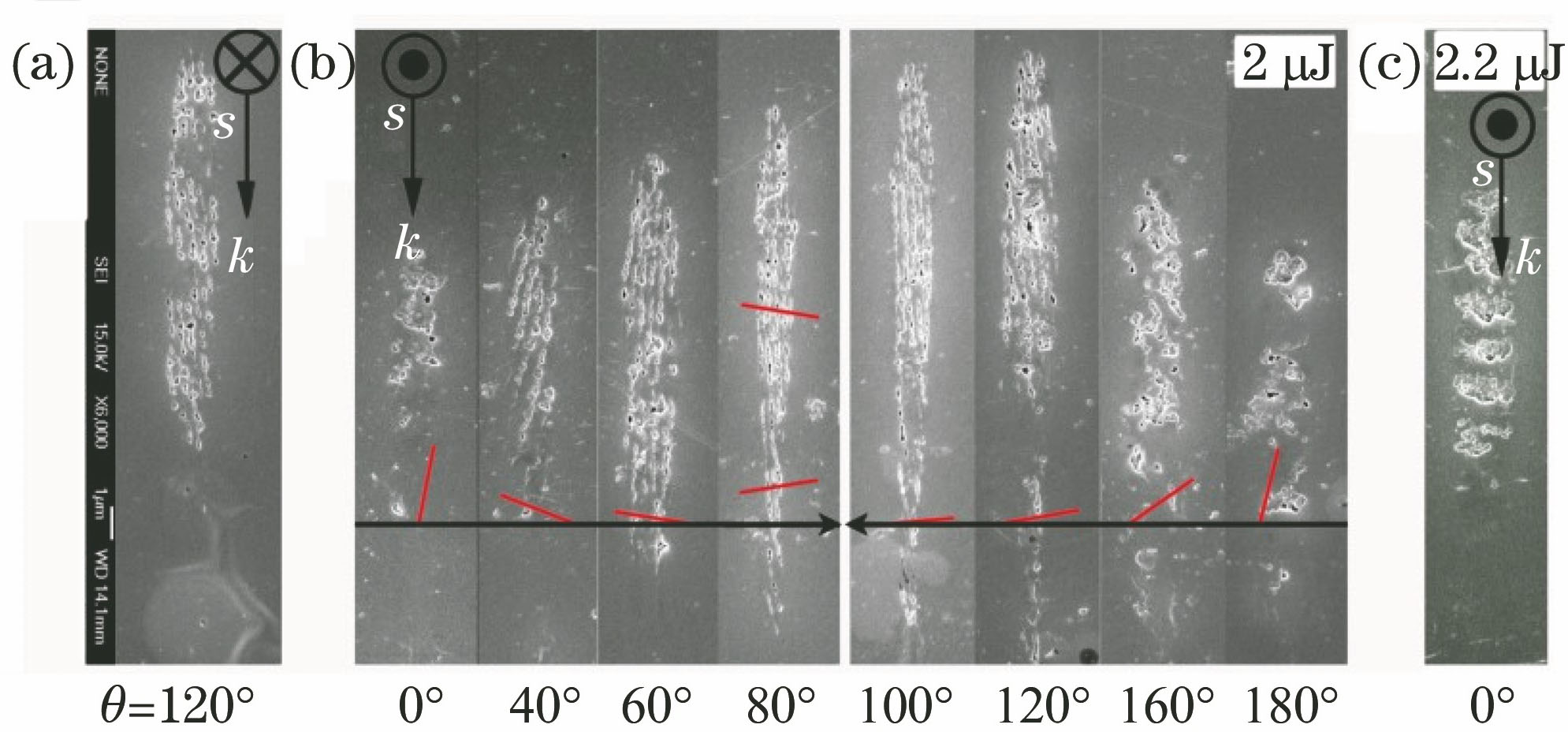
![SEM images of self-organized nano-gratings in the transversal cross section of written lines[42]](/richHtml/lop/2020/57/11/111402/img_1.jpg)
Fig. 1. SEM images of self-organized nano-gratings in the transversal cross section of written lines[42]
![SEM images of various designed suspended structures (line, disk, helix, and pentagon stuctures)[43]](/richHtml/lop/2020/57/11/111402/img_2.jpg)
Fig. 2. SEM images of various designed suspended structures (line, disk, helix, and pentagon stuctures)[43]
Fig. 3. Complicated 3D structures[44]. (a) Three-level steps; (b) the word “LASER” on a rectangular step; (c) rectangular pyramid; (d) concave micro lens array
Fig. 4. Bubbles induced at different FDs[9]
Fig. 5. Cross section of optical waveguide fabricated in Nd∶KGW[49]. A is the waveguide area, B is the filament induced by the femtosecond laser, and C is the unprocessed area (bulk) far away from the filament
Fig. 6. Femtosecond laser inscription of optical waveguide in SMF-NCF-SMF[50]
Fig. 7. Experimental setup for fabrication of ULPFBGs[51]
Fig. 8. Fabricated grating structure in the core of fiber[51]
Fig. 9. Microscope images of cross section of sapphire fiber and inscribed fourth-order SFBG[38]. (a) Microscope image of cross section of sapphire fiber with diameter of 60 μm; microscope images of inscribed fourth-order SFBG: (b) top view and (c) side view
Fig. 10. Schematic diagram of line-by-line scanning method[6]
Fig. 11. Photomicrographs of fabricated SFBG[6]. (a) Top view; (b) side view
Fig. 12. Four in-fiber mirrors[52]
Fig. 13. Same micro-structures made by different scanning methods[55]. (a) Raster mode; (b) vector mode
Fig. 14. Polymer waveguide integrated in the fibre micro-cavity[32]. (a) Top view of fabricated polymer waveguide integrated in fiber micro-cavity; (b) polymer waveguide with length of 60 μm; (c) polymer waveguide with length of 80 μm
Fig. 15. Fabrication process diagram of liquid polymer filled-cavity FP fiber sensing structure[33]
Fig. 16. Optical microscope images of polymerized grating[58]. (a) Before rinsing; (b) after rinsing
Fig. 17. Microstructure of spiral channels in glass[8]. (a) Diagram of spiral-shaped microchannel; (b) side view of etched spiral-shaped microchannel by HF acid inside glass; (c) side view of spiral-shaped microchannel after baking of etched sample at 600 ℃ for 4 h; (d) cross-section of post baked microchannel; (e) cross-section of channel at the opening area
Fig. 18. Side view of blue solution flowing through spiral-microchannel[8]
Fig. 19. Helical microchannel in quartz glass[71]. (a) Fabricated helical microchannel with block at end of channel; (b)(c) fabricated helical micro channels with length of 1 mm
Fig. 20. Structures of micro diverter and micro mixer[72]. (a) Empty micro mixer; (b) micro mixer filled with water; (c) empty micro diverter; (d) micro diverter filled with water
Fig. 21. Three-dimensional microfluidic chip[73]. (a) Diagram of microfluidic chip; (b) fabricated microfluidic chip in silica glass
Fig. 22. Fabricate micro channels in optic fibers using femtosecond laser-induced water break down[74]
Fig. 23. Structures of liquid refractive index sensor with three micro channels across fiber core[72]. (a) Front view; (b) top view; (c) opening of microchannel on the top of fiber; (d) opening of microchannel on the bottom of fiber
Fig. 24. H-type humidity sensor in SMF[76]. (a) Top view of fabricated two vertical micro channels rightly across fiber core; (b) side view of fabricated two vertical micro channels rightly across fiber core in SMF in the first step; (c) top view of fabricated H-type microchannel in SMF; (d) side view of fabricated H-type microchannel in SMF
Fig. 25. MZ interferometer microcavity in SMS fiber structure by femtosecond laser-induced water breakdown[78]. (a) A section of multi mode fiber was spliced between two sections of the SMF; (b) structure of SMS; (c) setup for fabricating microcavity in SMS by femtosecond laser-induced water breakdown; (d) scanning track of laser focus; (e) fabricated microcavity in SMS

Set citation alerts for the article
Please enter your email address


