• Journal of Semiconductors
  • Vol. 42, Issue 10, 101604 (2021)
Yiyi Zhu1、2, Qianpeng Zhang1、2, Lei Shu1、2, Daquan Zhang1、2, and Zhiyong Fan1、2、3
Author Affiliations
  • 1Department of Electronic & Computer Engineering, The Hong Kong University of Science and Technology, Hong Kong 999077, China
  • 2HKUST-Shenzhen Research Institute, Shenzhen 518057, China
  • 3Guangdong-Hong Kong-Macao Joint Laboratory for Intelligent Micro-Nano Optoelectronic Technology, HKUST, Hong Kong 999077, China
  • show less
    DOI: 10.1088/1674-4926/42/10/101604 Cite this Article
    Yiyi Zhu, Qianpeng Zhang, Lei Shu, Daquan Zhang, Zhiyong Fan. Recent progress of efficient flexible solar cells based on nanostructures[J]. Journal of Semiconductors, 2021, 42(10): 101604 Copy Citation Text show less

    Abstract

    Flexible solar cells are important photovoltaics (PV) technologies due to the reduced processing temperature, less material consumption and mechanical flexibility, thus they have promising applications for portable devices and building-integrated applications. However, the efficient harvesting of photons is the core hindrance towards efficient, flexible PV. Light management by nanostructures and nanomaterials has opened new pathways for sufficient solar energy harvesting. Nanostructures on top surfaces provide an efficient pathway for the propagation of light. Aside from suppressing incident light reflection, micro-structured back-reflectors reduce transmission via multiple reflections. Nanostructures themselves can be the absorber layer. Photovoltaics based on high-crystallinity nanostructured light absorbers demonstrate enhanced power conversion efficiency (PCE) and excellent mechanical flexibility. To acquire a deep understanding of the impacts of nanostructures, herein, a concise overview of the recent development in the design and application of nanostructures and nanomaterials for photovoltaics is summarized.

    1. Introduction

    Sunlight provides the most abundant sustainable energy to our world. Flexible thin-film photovoltaics (TF-PV) are important technologies in the PV community due to the reduced pay-back time[1] and material consumption[2]. Meanwhile, their lightweight and excellent mechanical flexibility are particularly suitable for portable and wearable power supply and building-integrated applications[2, 3]. Reducing solar radiation loss becomes the foremost concern to reach the requirement of efficient flexible solar cells[4, 5]. Whereas, the transparent dielectrics or metal oxide layer with a high refractive index produce an unfavored reflection. Researchers are searching for anti-reflection schemes to address this issue. Currently, the conventional quarter-wavelength (λ/4) coatings can be only effective for the photons at a typical wavelength under normal incidence[6-9]. To achieve enhanced broadband absorption, advanced light trapping techniques have been utilized. In industry, the pyramid structure or random textures are the most widely used light-trapping techniques for textured crystalline silicon solar cells[10, 11]. However, this micro-sized texturing is not an option for TF-PV with only several hundred nanometers thick active layers.

    The utilization of nanostructures for advanced light management is a realistic path to minimize optical losses of TF-PV. Implementing these nano/microstructures, for instance, nano/micro-pyramid[5], nanowire (NW)[10, 12-14], nanopillar[15, 16], nanocone (NC)[17], nano dome[18], nanosphere[19, 20], nanobowl (NB)[21], and nanosheets (NSs)[22] on solar cells contribute to several times enhancement of short-circuit current (Jsc)[23]. In the meantime, effectively improved light-harvesting makes the utilization of ever-thinner cells possible. Thereby, a larger proportion of carriers can reach the boundary and be separated into free carriers before recombination. The reduced collection path potentially results in enhanced open-circuit voltage (Voc)[4].

    It is highly desirable to have a nanostructured film with broadband anti-reflection and self-cleaning capacity on the top surface of solar panels for real application. As the incident angle of sunlight varies during the day, the angular dependence performance determines a solar cell's daily electrical energy output[24]. Considerable study has already confirmed that the utilization of nanostructures effectively improves output power over a broad range of incident angles. Besides, there is a need for manpower to maintain the surface cleaning of solar panels in outdoor conditions, as the dust stuck on the solar panels will block the solar radiation and lead to performance degradation. The nanostructured film with the function of self-cleaning capacity becomes a practical solution to this issue[25-27].

    The active layer itself can also be nanostructured. Taking one-dimensional (1D) NW, for example, photovoltaics based on high crystallinity (even monocrystalline) NW provide remarkable improvement in PCE. One contributing factor is the sufficient photogenerated carrier generation and collection in optoelectronic nanodevice[28]. Meanwhile, the single crystallinity of NW is beneficial to form a direct charge transport pathway, which makes carrier mobility several orders of magnitudes outperform polycrystallinity TF counterpart[29]. Additionally, nanostructured devices are considered ideal structures for studying geometry's effect on optoelectronic and mechanical properties. Massive work has already demonstrated their merits in flexibility in an assortment of highly flexible optoelectronic device[7].

    This review provides a comprehensive review of the recent developments in various light management nanostructures for photovoltaics. In particular, we focus on nanostructures on top as a broadband anti-reflection layer with self-cleaning capacity and survey micro-structured back-reflectors to reduce transmission via multiple reflections. We also summarize the recent progress in developing flexible photovoltaics based on NW with improved bendability, longevity, and PCE. The distinct merits and challenges of these strategies are discussed.

    2. Nanostructures at the front surface

    It is known that there are two categories of absorption losses: reflection and transmission. The transparent dielectrics or metal oxide layer with a high refractive index produce an unfavored reflection. One practical solution to minimize reflection is the nanostructures implemented on the top surface of solar panels. Nanostructures offer an efficient pathway for the photons flux and reduce solar radiation power loss due to the antireflection effect from the geometry and gradual refractive index gradient provided by nanostructures[
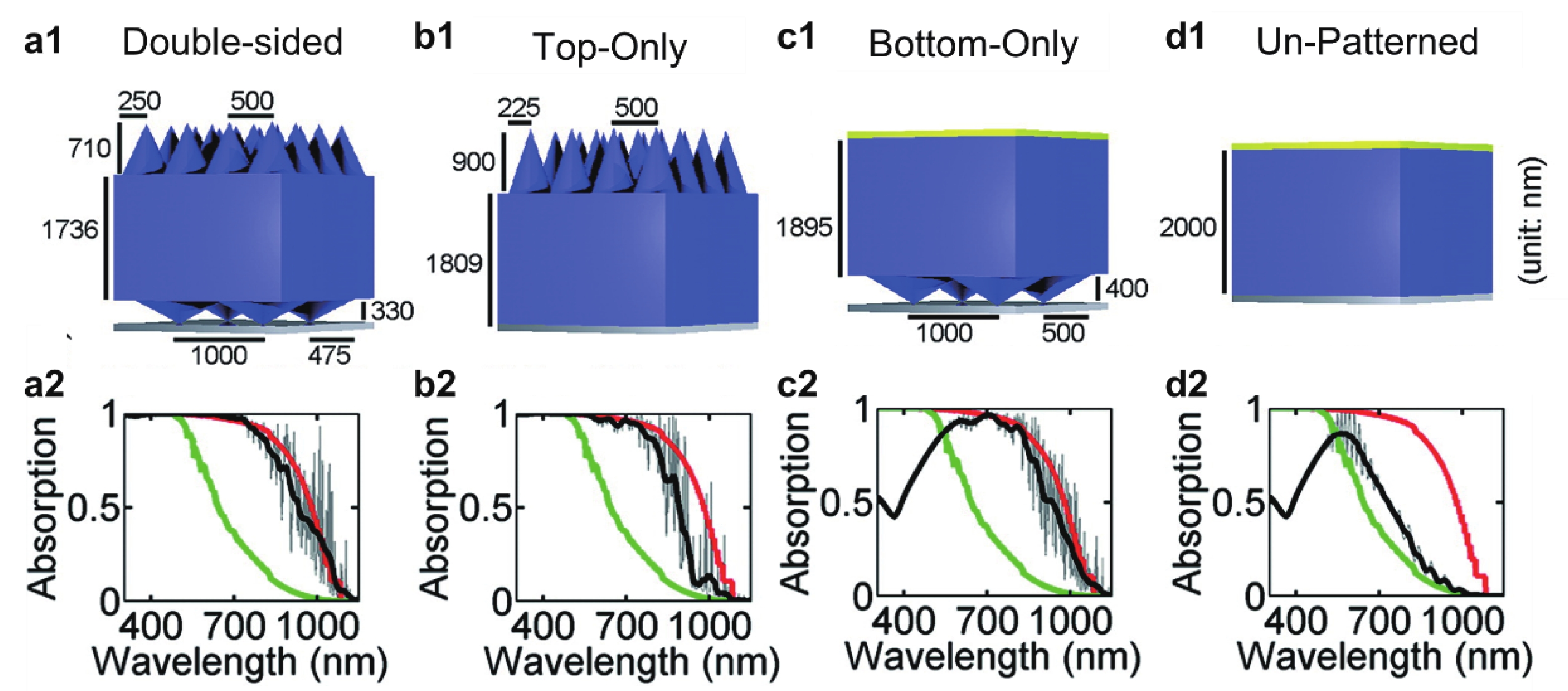
4]. Careful modification of the shape and size of nanostructures provides new degrees of light manipulation. Theoretical calculations have been performed to maximize absorption in cells. Fig. 1(a1) is the typical prototype of PV consisting of nanostructures on top for light-trapping and a back-reflector at the bottom[30]. The simulated light absorption of the optimum structure is close to the Yablonovitch limit (Fig. 1(a2)). By comparison, shown in Fig. 1(b1), only the high-aspect-ratio, dense nanostructure arrays are utilized in the front, working as an anti-reflection layer. Most photons at short wavelengths, from 400 to 500 nm, are fully absorbed in the single path of semiconductors. This makes the antireflection on the top surface more critical for these wavelengths (Fig. 1(b2))[31]. Fig. 1(c1) shows the low-aspect-ratio, low-density microstructure arrays used in the back to reflect light into the light active layer. As shown in Fig. 1(d), for the neat TF, the light-harvesting of photons decreases with increasing wavelength. Thus, multiple reflections from the back reflector in Fig. 1(c1) improve optical path length for the photons at the wavelength near the bandgap. The theoretical calculation, Fig. 1(c2), shows that the microstructure arrays significantly improve light absorption at the wavelength of 0.8–1.1 µm compared with the planar counterpart.

    (Color online) Three-dimensional (3D) nanostructured silicon solar cells and their corresponding absorption spectra. (a1, a2) Double-sided nanostructure. (b1, b2) Top-only nanostructure. (c1, c2) Bottom-only nanostructure. (d1, d2) Flat film. Red curves stand for the Yablonovitch limit, green curves are the single-pass absorption spectra, and black curves represent spectra for corresponding structures. Reproduced with permission[31]. Copyright 2014, Wiley-VCH.

    Figure 1.(Color online) Three-dimensional (3D) nanostructured silicon solar cells and their corresponding absorption spectra. (a1, a2) Double-sided nanostructure. (b1, b2) Top-only nanostructure. (c1, c2) Bottom-only nanostructure. (d1, d2) Flat film. Red curves stand for the Yablonovitch limit, green curves are the single-pass absorption spectra, and black curves represent spectra for corresponding structures. Reproduced with permission[31]. Copyright 2014, Wiley-VCH.

    Apart from the light-trapping effect, wavelength-scale nanospheres can diffractively couple photons and assist confined resonant modes. Moreover, owning to whispering gallery resonances within the spheres, the light coupling between the spheres is witnessed in the highly periodic array of dielectric nanospheres[32-36]. These will significantly enhance the optical path length inside the light absorber[4].

    Tsui et al. reported a cost-effective method for flexible plastic with three-dimensional (3D) light-trapping nanocone (NC) arrays[25]. Figs. 2(a) and 2(b) show the scanning electron microscopy (SEM) images of inverse NC template and NC arrays, respectively. Tsui et al. illustrate the modification of NC arrays morphology, such as pitch and height, via changing the template's geometry. Notably, the NC arrays films are adhesive-free and easily attached to substrates, including glass and silicon. A noticeable light-trapping enhanced performance is observed in the optical measurements and theoretical simulations. This is further confirmed in Fig. 2(c) external quantum efficiency (EQE) measurements of CdTe solar cells. In addition, their nanostructures also possess broadband light trapping capability[37]. This is confirmed in the daily electrical energy output measurement. After implementing anti-reflection films, the output of CdTe solar cells reaches as high as 1 kW·h/m2, showing 7% enhancement compared with the control group[25]. Similarly, Tang et al. proposed a large-scale manufacturing approach of adhesive-free, 3D NC structured flexible, and anti-reflection films[26]. As expected, the antireflection NC arrays effectively boost light-harvesting, verified in finite-difference time-domain (FDTD) simulations.

    The scanning electron microscope (SEM) of inverse nanocone (NC) template (a) and NC arrays (b). (c) The external quantum efficiency (EQE) spectra of CdTe solar cells with and without NC film. The inset of (c) is the schematic structure of the device. (a–c) Reproduced with permission[25]. Copyright 2014, Wiley-VCH. (d) SEM of NC arrays. The inset is a drop of water on NC arrays, illustrating a contact angle of 155°. (e) The current density–voltage (J–V) characteristics of perovskite solar cells with and without NC arrays (inset is a photo of the flexible device). (f) Under different incident angles, the short-circuit current density (Jsc) and the power conversion efficiency (PCE) with and without NC arrays. (d–f) Reproduced with permission[38]. Copyright 2015, American Chemical Society. (g) Schematic procedure of 3D nanostructured a-Si:H solar cells. (1) Spin coating ZnO film on polyimide film. (2) Patterned ZnO film. (3) A a-Si:H solar cell constructed on the as-fabricated substrate. (4) Fabrication of nanoindentation on aluminum foils. (5) The anodic aluminum oxide (AAO) template with inverse NC arrays. (6) The NC arrays film peeled off from the template. (7) The a-Si:H solar cell with nanostructured back-reflector and top anti-reflection NC arrays. (h) Normalized PCE under different bending angles. (i) Normalized PCE as a function of bending cycles. The insets (h) and (i) demonstrate bending angles and a bent solar cell mounted on the set-up. Reproduced with permission[39]. Copyright 2017, Wiley-VCH.

    Figure 2.The scanning electron microscope (SEM) of inverse nanocone (NC) template (a) and NC arrays (b). (c) The external quantum efficiency (EQE) spectra of CdTe solar cells with and without NC film. The inset of (c) is the schematic structure of the device. (a–c) Reproduced with permission[25]. Copyright 2014, Wiley-VCH. (d) SEM of NC arrays. The inset is a drop of water on NC arrays, illustrating a contact angle of 155°. (e) The current density–voltage (J–V) characteristics of perovskite solar cells with and without NC arrays (inset is a photo of the flexible device). (f) Under different incident angles, the short-circuit current density (Jsc) and the power conversion efficiency (PCE) with and without NC arrays. (d–f) Reproduced with permission[38]. Copyright 2015, American Chemical Society. (g) Schematic procedure of 3D nanostructured a-Si:H solar cells. (1) Spin coating ZnO film on polyimide film. (2) Patterned ZnO film. (3) A a-Si:H solar cell constructed on the as-fabricated substrate. (4) Fabrication of nanoindentation on aluminum foils. (5) The anodic aluminum oxide (AAO) template with inverse NC arrays. (6) The NC arrays film peeled off from the template. (7) The a-Si:H solar cell with nanostructured back-reflector and top anti-reflection NC arrays. (h) Normalized PCE under different bending angles. (i) Normalized PCE as a function of bending cycles. The insets (h) and (i) demonstrate bending angles and a bent solar cell mounted on the set-up. Reproduced with permission[39]. Copyright 2017, Wiley-VCH.

    The energy output of solar cells can be interfered with or even cut down by the dust on the top of solar modules when it comes to outdoor conditions, especially in the solar farm located in the desert. The dust stuck on solar panels will block the solar radiation and lead to performance degradation. Therefore, there is a need for manpower or machine to maintain the surface cleaning of solar panels. Apart from the constant maintenance cost, an abundant amount of water is needed to clean the solar system that is precious in the desert area. The nanostructured film with the function of self-cleaning capacity becomes a practical solution to this issue[25-27].

    Tavakoli et al. fabricated flexible perovskites solar cells on ultrathin willow glass substrates with polydimethylsiloxane (PDMS) NC array films on top as a light-trapping and self-cleaning layer[38]. Illustrated in Fig. 2(d), the NC array demonstrates a depth and opening width of 1 μm. Besides, as shown in the inset of Fig. 2(d), the NC structure demonstrates a water-repellent capacity, with a high water contact angle of 155°, suggesting a self-cleaning function. To further confirm the self-cleaning property, the experiment is carried out by spreading the sand on the top surface of solar cells. The dust is easy to remove by rolling a water droplet across the surface, compared with the device without nanostructures. Fig. 2(e) is the current density–voltage (J–V) characteristics of flexible solar cells with and without the NC array under simulated AM1.5G illumination. The inset is a photograph of a perovskite solar cell based on flexible willow glass. A noticeable enhanced Jsc from 17.7 to 19.3 mA/cm2 is observed after applying the NC structure. This leads to PCE improvement from 12.06% to 13.14%, corresponding to ~9% increment. The improved performance is also witnessed under oblique light, which is critical for the solar cell's daily operation, as the sunlight varies during the day. Fig. 2(f) is the angular-dependent performance of Jscand PCE of the device with and without the NC array. To have a fair comparison with conditions where the device is not inclined under the collimated irradiation, both Jsc and PCE measured under different incident angles are normalized with the horizontal light projection area. Clearly, the improvement ofJsc and PCE of NC-based devices is around 1.5–2.5 mA/cm2 and 1%–1.75%, respectively. Notably, both Jsc and PCE drop more notably with the increase of incident angle for the control group than the case with NC structure.

    Similarly, through nanoimprinting lithography, Zhang et al. realized highly ordered metal oxide nanotextures on polyimide (PI) substrate for the highly flexible amorphous silicon (a-Si:H) solar cells[39]. Fig. 2(g) shows the fabrication process of a-Si:H solar cells on patterned ZnO/PI substrates covered with NC structures. Briefly, the back reflector ZnO films with highly ordered nanoholes arrays are fabricated through nanoimprinting lithography. Then, a-Si:H solar cells are constructed on the patterned PI flexible substrates. The anodic aluminum oxide (AAO) film is used as a template to pattern NC arrays film that is attached on the top of a-Si:H solar cell. Benefitting from the sufficient light absorption, the PCE of the nanostructured device increased up to 8.17%, which is nearly 48.5% improvement over the planar control group. To evaluate the mechanical robustness, shown in Fig. 2(h), the PCE of the device under bending angles from 0° to 180° are characterized[40]. The PCE is normalized by the projection area. Notably, the NC-based devices only encounter 17% PCE drop under the bending angle of 180°. As shown in Fig. 2(i), the periodic nanopatterns contribute to better excellent flexibility. NC-based devices only experience a negligible drop in PCE after 100 000 bending cycles. Zhang et al. attributed the excellent mechanical flexibility to the nanostructure, effectively minimizing the strain and stress generated during bending. Because the strain and stress raise the possibility of crack nucleation and delamination at the interface, leading to performance degradation.

    3. Nanostructures at the back surface

    As mentioned above, antireflection coatings affect the optical loss caused by reflection. In contrast, light-trapping schemes address the loss by transmission. Especially, photons at the longer wavelength are less absorbed in the single path because of decreased absorption with increasing the wavelength towards the bandgap[31].

    The loss of light absorption in the red region is the cause of undesired reddish-brown color for conventional semi-transparent perovskite solar cells (ST-PSCs) based on the continuous TF[41-48]. The reddish-brown hue is unfavored for the application of power-generated windows for building-integrated photovoltaics[49]. The periodic arrays of microstructure implemented at back work as reflectors to increase the optical path length through multiple reflections. Besides, the reflection and angular distributions of the scattered light can be controlled by geometry modification, for instance, shape, diameters, and periodicities. With this regard, in Fig. 3(a), Zhu et al. proposed a moth-eye-inspired structure (MEIS) for ST-PSCs[50]. Fig. 3(b) is the reflection spectra of MEIS. The biomimetic structure is a perfect back reflector that only reflects photons in the wavelength range where the human eye is less discerning. This is further confirmed in the inset of Fig. 3(b) that the patterned area only reflects blue and red light. In Fig. 3(c), the unique optical property contributes to the improvements in ST-PSCs performance without compromising the average visible transmittance (AVT). MEIS device raises PCE to 10.53% at AVT of 32.50%, which is a significant improvement compared to the planar counterpart (PCE = 8.78%, AVT = 35.00%). Thus, a record high figure-of-merit for ST-PSCs, defined as the product of PCE and AVT, is achieved. Besides, confirmed by the inset of Fig. 3(c), the improved light-harvesting in the longer wavelength helps convert visual appearance from the reddish-brown (planar control group) to a desired near-neutral color (MEIS).

    (Color online) (a) Complete compound moth eyes and a moth-eye-inspired structure (MEIS) device structure diagram. (b) Reflectance spectra of MEIS and human luminosity curve, inset is the photo of MEIS (scale bars, 3 cm). (c) J–V curves of the MEIS ST-PSCs and a planar reference under simulated AM1.5G illumination, the inset is the photographs of (c) (scale bars, 2 cm). Reproduced with permission[50]. Copyright 2021, Wiley-VCH. (d) SEM images of TiO2 nanobowl with a diameter of 180 nm (NB-180). (e) J–V curves of the device based on different diameters. (f) Simulated cross-sectional |E| distribution of the electromagnetic (EM) waves at 600 nm wavelength in the perovskite deposited on (f1) TiO2 NB-180, (f2) TiO2 NB-220, (f3) TiO2 NB-500, and (f4) planar TiO2, Reproduced with permission[21]. Copyright 2021, Wiley-VCH. (g) Schematic view of nanostructured a-Si:H thin-film. (h) SEM image of the 100 nm Ag-coated substrates deposited with 100 nm conductive Al-doped ZnO (AZO). (i) The calculatedJsc of the device based on different diameters TiO2. (j) Normalized PCE under different bending angles. The inset (j1) represents a photo of the measurement set-up and (j2) a schematic of bending angles. Reproduced with permission[40]. Copyright 2021, Wiley-VCH.

    Figure 3.(Color online) (a) Complete compound moth eyes and a moth-eye-inspired structure (MEIS) device structure diagram. (b) Reflectance spectra of MEIS and human luminosity curve, inset is the photo of MEIS (scale bars, 3 cm). (c) J–V curves of the MEIS ST-PSCs and a planar reference under simulated AM1.5G illumination, the inset is the photographs of (c) (scale bars, 2 cm). Reproduced with permission[50]. Copyright 2021, Wiley-VCH. (d) SEM images of TiO2 nanobowl with a diameter of 180 nm (NB-180). (e) J–V curves of the device based on different diameters. (f) Simulated cross-sectional |E| distribution of the electromagnetic (EM) waves at 600 nm wavelength in the perovskite deposited on (f1) TiO2 NB-180, (f2) TiO2 NB-220, (f3) TiO2 NB-500, and (f4) planar TiO2, Reproduced with permission[21]. Copyright 2021, Wiley-VCH. (g) Schematic view of nanostructured a-Si:H thin-film. (h) SEM image of the 100 nm Ag-coated substrates deposited with 100 nm conductive Al-doped ZnO (AZO). (i) The calculatedJsc of the device based on different diameters TiO2. (j) Normalized PCE under different bending angles. The inset (j1) represents a photo of the measurement set-up and (j2) a schematic of bending angles. Reproduced with permission[40]. Copyright 2021, Wiley-VCH.

    Similarly, to address the insufficient light-harvesting, Zheng et al. proposed a strategy of TiO2 nanobowl (NB) array with controlled morphology and fabricated carbon cathode-based perovskite solar cells[21]. Fig. 3(d) shows the top-view and cross-section view SEM of the TiO2 NB array. TiO2 NB array is a light-trapping layer to quench photons and thereby reduce transmission and boost absorption. Fig. 3(f) reveals the J–V curves of TiO2 NB-based devices and planar counterparts. As expected, enhanced performance is achieved in the TiO2 NB-based devices compared with the planar counterpart. The contributing factor for the improved performance is enhanced light absorption arising from the NB back reflector. To study the light management, shown in Fig. 3(f), the cross-sectional electric field intensity (|E|) distributions of the electromagnetic (EM) wave at 600 nm are calculated. Interestingly, the TiO2 NB-based devices reveal stronger electric field intensity than the planar control group, resulting from a larger proportion of photons coupled into the TiO2 NB array.

    Xiao et al. systematically investigated the performance of a-Si:H solar cells based on the different thicknesses of oxide spacer layers[40]. The nanopatterned Al is used as the substrate, and the device structure is shown in Fig. 3(g). The corresponding SEM image of the substrates coated with 100 nm Ag/100 nm conductive Al-doped ZnO (AZO) is represented in Fig. 3(h). Interestingly, the increased thickness of the spacer layer AZO reduces the absorption in the Ag layer and induces enhanced light-harvesting in the silicon layer in return. As shown in Fig. 3(i), the highest calculated current density in the silicon layer is witnessed in the device based on the 100 nm spacer layer (ND100 device). This suggests that the light-harvesting of the nanopatterned device can be rationally controlled by modification of device geometry. More importantly, aluminum foils hold large-scale manufacturing possibilities and excellent mechanical flexibility[51, 52]. Shown in Fig. 3(j), the normalized PCE of the ND100 device under different bending angles is measured. The PCE only encounter a negligible 8.8% drop even under the bending angle of 120°.

    4. 3D nanostructured device

    4.1. 3D nanostructured for light management & boosted carrier collection

    The most crucial part of photovoltaics is the adequate harvesting of photons, exciting electrons to the conductive band, and leaving holes behind. Nanomaterials provide the opportunity to minimize loss of each step, for instance, absorption, carrier generation, separation, and collection. Besides, the nano-scale geometry offers unique advantages, including suppressed reflection, light trapping, facile strain relaxation, new charge separation mechanisms, better defect tolerance, etc.[53]. These advantages are not expected to improve the PCE above the standard limits. Instead, nanotechnology decreases the quantity and quality of material requirements to obtain a highly efficient device[54]. The solar cells based on nanopillar-array with radial p–n junctions are an excellent example of this point.

    In Figs. 4(a) and 4(b), Fan et al. pioneered a nanopillar-array CdTe/CdS photovoltaics with a 3D geometric configuration[28]. The 3D device structure affords effective radial charge collection and light absorption[10, 13, 55]. The experimental result Fig. 4(c) and simulation calculations Fig. 4(d) show that absorption is improved in 3D nanodevice. One contributing factor is that 3D geometric configuration reduces reflection and thereby enhances optical absorption. In addition, the 3D nanopillar array offers excellent light absorption along the length of the wire[15, 38].

    (Color online) (a) Cross-sectional schematic diagram of a 3D solar nanopillar cell, demonstrating improved carrier separation and collection. (b) SEM images of d a CdS nanopillar array. The experimental (c) and simulated (d) absorption spectra of the nanowire (NW) plotted as a function of diameter and pitch. (c, d) Reproduced with permission[15]. Copyright 2012, American Chemical Society. (e) SEM images of InSb NW. (f) The electron mobility of InSb NW. (e, f) Reproduced with permission[58]. Copyright 2019, American Chemical Society. (g) Visualization of the Shockley–Read–Hall (SRH) recombination in the 3D nanopillar cells plotted with a function of heigh (H): H = 0 nm (g1) and H = 900 nm (g2). (a, b, g) Reproduced with permission[28]. Copyright 2009, Nature Research. (h) Schematic representation of BiI3 structure. (h) Reproduced with permission[75]. Copyright 2017, Wiley-VCH. (i) Cross-sectional schematic diagram of 3D BiI3 nanosheets (NSs) cell. (j) SEM of BiI3 NSs. (k) J–V curves of BiI3 NSs solar cells from different precursor Bi thicknesses. (i–k) Reproduced with permission [22]. Copyright 2020, Wiley-VCH.

    Figure 4.(Color online) (a) Cross-sectional schematic diagram of a 3D solar nanopillar cell, demonstrating improved carrier separation and collection. (b) SEM images of d a CdS nanopillar array. The experimental (c) and simulated (d) absorption spectra of the nanowire (NW) plotted as a function of diameter and pitch. (c, d) Reproduced with permission[15]. Copyright 2012, American Chemical Society. (e) SEM images of InSb NW. (f) The electron mobility of InSb NW. (e, f) Reproduced with permission[58]. Copyright 2019, American Chemical Society. (g) Visualization of the Shockley–Read–Hall (SRH) recombination in the 3D nanopillar cells plotted with a function of heigh (H): H = 0 nm (g1) and H = 900 nm (g2). (a, b, g) Reproduced with permission[28]. Copyright 2009, Nature Research. (h) Schematic representation of BiI3 structure. (h) Reproduced with permission[75]. Copyright 2017, Wiley-VCH. (i) Cross-sectional schematic diagram of 3D BiI3 nanosheets (NSs) cell. (j) SEM of BiI3 NSs. (k) J–V curves of BiI3 NSs solar cells from different precursor Bi thicknesses. (i–k) Reproduced with permission [22]. Copyright 2020, Wiley-VCH.

    The carrier separation and collection advantages of the radial geometry are more noticeable. As the single crystallinity of nanopillar (Figs. 4(e) and 4(f)) is beneficial to form guiding channels for carriers, the direct charge transport pathway makes electron mobility in NWs several orders of magnitude higher than in the polycrystallinity TF counterpart[29, 56-58]. More importantly, the orthogonal carrier collection in the radial built-in electric field (Fig. 4(a)) benefits photogenerated carrier collection[28]. The photogenerated carrier only needs to travel a short path and reach the boundary of p–n junctions. This is especially beneficial for photovoltaic materials with a short diffusion length[59].

    To achieve the optimum performance cell, the detailed optimization of the optical and electronic properties is required, which are strongly determined by the geometry of the nanopillar[60]. To investigate the dependency of the performance on the geometric configuration, the theoretical simulations of Shockley–Read–Hall (SRH) recombination as a function of height (H) are carried out. The visualization of SRH recombination for H = 0 nm (Fig. 4(g1)) and H = 900 nm (Fig. 4(g2)) is plotted. Notably, as shown in Fig. 4(g1), the space charge and carrier collection region are quite low for H = 0 nm. This leads to a large proportion of photogenerated carriers lost in the upper portion of the film via recombination, where there is a high level of photogenerated carrier generation. However, as shown in Fig. 4(g2), the space charge and carrier collection region are dramatically improved for H = 900 nm. This decreased the total volumetric recombination in return. However, the nanostructure may lead to a drop in PCE in contrast to planar counterparts when surface recombination is the limiting factor.

    Multilayered photovoltaic absorbers, such as BiI3, two-dimensional (2D) perovskites, and transition metal dichalcogenides have gained enormous attention because of their unique properties. Shown in Fig. 4(h), BiI3 is a layered 2D material constructed by the repeating unit of the I-Bi-I layer. Carriers are mobile in the layer and immobile across planes[22]. The carrier transport and collection in the randomly oriented polycrystalline TF is insufficient, which is the core hindrance for high-performance photovoltaics based on 2D materials. To tackle this issue, Zhu et al. fabricated 3D BiI3 nanosheets (NSs) based photovoltaics that embeds vertically aligned monocrystalline BiI3 NSs into 2,2’,7,7’-Tetrakis[N, N-di(4-methoxyphenyl)amino]-9,9’-spirobifluorene (spiro-OMeTAD)[22]. It is noteworthy that vertically aligned monocrystalline BiI3 NSs are directly fabricated on the substrate with a controlled geometric configuration through the vapor-solid-solid reaction. The direct growth of nanomaterial on the substrate reduces production costs. Fig. 4(i) shows the cross-sectional schematic diagram of the BiI3 NSs cell. BiI3 NSs are embedded into spiro-OMeTAD to form the 3D heterojunction. The top-view SEM image of vertically aligned monocrystalline BiI3 NSs is shown in Fig. 4(j). Light is prevented from bouncing off the top surface and coupling light in the nanostructured active layer. BiI3 NSs based device shows one magnitude lower in the light reflection over a planer reference. This is further confirmed in the J–V curve measurement. The experimental result Fig. 4(k) shows that Jsc is significantly improved compared with a planar reference due to less trap-assisted recombination in the monocrystalline BiI3 and large p–n junction areas of 3D heterojunction structure[10, 61, 62]. As a result, a record-high PCE of 1.45% is achieved (Fig. 4(k)). Notably, the BiI3 NSs-based device demonstrates robust stability against moisture and oxygen, resulting from the self-passivated surface of monocrystalline BiI3 NSs. The non-packaged device retained 96% of the original PCE after 24 h of continuous AM 1.5 illumination at ~70% humidity and 82% of the initial PCE after one-month storage at ~30% humidity.

    4.2. 3D nanostructured devices for better flexibility

    High-performance flexible electronics increasingly gained attention during recent decades, owing to the promising potential in building-integrated photovoltaics, portable and wearable power supplies, etc.[63-65]. Various flexible active materials, such as amorphous silicon and organic semiconductors, have been studied for flexible electronics[66-68]. However, owing to the traps in amorphous silicon and the long-term stability of organic material, searching for a new candidate for flexible electronics is still the need of the hour[69, 70].

    For flexible photovoltaics, the bending and stretching of the device should not have a notable impact on PCE[71]. Currently, the dominant TF flexible photovoltaic suffers from rapid performance degradation during continuous bending. Nanodevice can effectively relax tensile and compressive stresses and avoid the formation of cracks during bending and stretching. They have demonstrated their merits in flexibility in an assortment of highly flexible optoelectronic devices[7].

    In Fig. 5, Leung et al. fabricated flexible, nanospike arrays of Al substrate for single-junction a-Si:H solar cells[52]. The fabrication process is shown in Fig. 5(a). By systematic analysis of the geometry, Leung et al. resolve the dilemma between light-harvesting and surface recombination. After the geometry optimization, a PCE of 7.92% is achieved. In addition, as illustrated in Fig. 5(b), the nanostructured device exhibits superior angular-dependent performance. The daily integrated power is 32% outperformed the planar counterpart. Fig. 5(c) is the mechanical stability test. The device based on nanospike arrays maintains 82% of original PCE remains after 1000 cycles. This type of nanostructures combines versatile merits in terms of excellent flexibility, lightweight, and cost-effectiveness.

    (Color online) (a) Schematic diagram of the 3D nanospike. (b) Angular and wavelength-dependent absorption of a nanospike solar cell and a planar reference. (c) Normalized PCE of the nanospike device under different bending angles, inset is the schematic of a flexible nanospike solar cell. (a–c) Reproduced with permission[52]. Copyright 2014, The Royal Society of Chemistry. (d) SEM image of a-Si:H solar cells on 0.5 aspect ratio nanocone. The aspect ratio is the ratio between height and pitch. Simulated cross-sectional stress distribution of flat (e) and nanocone devices (f), with their photos after bending with a radius of 4 mm shown. (d–f) Reproduced with permission[73]. Copyright 2016, The Royal Society of Chemistry.

    Figure 5.(Color online) (a) Schematic diagram of the 3D nanospike. (b) Angular and wavelength-dependent absorption of a nanospike solar cell and a planar reference. (c) Normalized PCE of the nanospike device under different bending angles, inset is the schematic of a flexible nanospike solar cell. (a–c) Reproduced with permission[52]. Copyright 2014, The Royal Society of Chemistry. (d) SEM image of a-Si:H solar cells on 0.5 aspect ratio nanocone. The aspect ratio is the ratio between height and pitch. Simulated cross-sectional stress distribution of flat (e) and nanocone devices (f), with their photos after bending with a radius of 4 mm shown. (d–f) Reproduced with permission[73]. Copyright 2016, The Royal Society of Chemistry.

    Tavakoli et al. reported efficient, flexible, and mechanically robust organometallic perovskite solar cells on plastic substrates with inverted NC structures[72]. PCE of 11.29% is achieved in the NC-based device, a 37% improvement from the planar control group. The mechanical simulation demonstrates that the NC structures contribute to relaxing stress and strain during continuous bending and suppressing cracks formation due to the sub-micrometer diameters. The NC-based device retained 90% of the original PCE after 200 mechanical bending cycles. In comparison, the planar group dropped to 60% of the initial PCE under the same condition.

    In Fig. 5(d), Lin et al. present a cost-effective approach towards periodical NC arrays of polyimide (PI), which possesses excellent mechanical flexibility and unique optical management[73]. The flexible a-Si:H solar cells are made on the nanopatterned PI substrate. Fig. 5(d) shows the top-view and cross-sectional view SEM images of the device. The a-Si:H devices demonstrate magnificent conformality and uniformity. Their result further confirmed that nanostructures are beneficial to release stress, which is verified in both the mechanical simulation and experimental observations of Figs. 5(e) and 5(f). Similarly, Linet al. reported flexible a-Si:H solar cells with a 3D nanostructure light-trapping scheme[74]. Apart from improved Jsc, excellent flexibility is achieved. The device maintained 97.6% of the initial efficiency even after 10 000 bending cycles.

    5. Summary and outlook

    Nanostructures and nanomaterials possess promising potential to improve the light-harvesting capability of solar cells. Nanostructures on the top surface offer broadband anti-reflection and self-cleaning capacities for solar cells. More importantly, the device's overall performance has been remarkably upgraded via implementing these nanostructures. Nevertheless, it is still far from the terminal objectives of the entire solar spectrum coverage for solar cells. Future work still requires optimizing geometry design and fabrication process to draw out the full potency of these light-trapping strategies.

    The nanostructured light absorbers offer photovoltaics unique optoelectronic and mechanical properties. The 3D geometric configuration leads to sufficient orthogonalization light-harvesting and carrier collection achieved in nanodevice. Also, nanodevices possess excellent mechanical highly flexibility. Despite the promising potential, surface recombination is the core hindrance for a high-performance nanodevice. Thus, the investigation of the surface property of material really matters. In this perspective, efforts are required to understand better the carrier dynamics at the surface, such as charge transfer, surface recombination, minority carrier diffusion, dopant density, surface state, and conductivity measurements. It is noteworthy that the PCE relies on efficient photogenerated carrier collection. The nanodevices' performance can be significantly improved through interface engineering for better surface quality and interfacial band alignment. Therefore, to explore the potentiality of nanodevice, efforts should be devoted to nanodevice geometry design, material choice, surface passivation/treatments, and energy-level alignment engineering.

    Acknowledgments

    This work was supported by the National Natural Science Foundation of China (Project No. 51672231), the Science and Technology Plan of Shenzhen (Project Nos. JCYJ20170818114107730, JCYJ20180306174923335), the General Research Fund (Project Nos. 16309018, 16214619) from the Hong Kong Research Grant Council. Guangdong-Hong Kong-Macao Intelligent Micro-Nano Optoelectronic Technology Joint Laboratory (Project No. 2020B1212030010), HKUST Fund of Nanhai (Grant No. FSNH-18FYTRI01). The authors also acknowledge the support from the Center for 1D/2D Quantum Materials and the State Key Laboratory of Advanced Displays and Optoelectronics Technologies at HKUST and Foshan Innovative and Entrepreneurial Research Team Program (2018IT100031).

    References

    [1] A V Shah, R Platz, H Keppner. Thin-film silicon solar cells: A review and selected trends. Sol Energy Mater Sol Cells, 38, 501(1995).

    [2] Q F Lin, H T Huang, Y Jing et al. Flexible photovoltaic technologies. J Mater Chem C, 2, 1233(2014).

    [3] M B Schubert, J H Werner. Flexible solar cells for clothing. Mater Today, 9, 42(2006).

    [4] M L Brongersma, Y Cui, S Fan. Light management for photovoltaics using high-index nanostructures. Nat Mater, 13, 451(2014).

    [5] B Hua, Q F Lin, Q P Zhang et al. Efficient photon management with nanostructures for photovoltaics. Nanoscale, 5, 6627(2013).

    [6]

    [7] Q Zhang, D Zhang, L Gu et al. Three-dimensional perovskite nanophotonic wire array-based light-emitting diodes with significantly improved efficiency and stability. ACS Nano, 14, 1577(2020).

    [8] K Ramanathan, M A Contreras, C L Perkins et al. Properties of 19.2% efficiency ZnO/CdS/CuInGaSe2 thin-film solar cells. Prog Photovolt: Res Appl, 11, 225(2003).

    [9] B S Richards. Comparison of TiO2 and other dielectric coatings for buried-contact solar cells: A review. Prog Photovolt: Res Appl, 12, 253(2004).

    [10] E Garnett, P D Yang. Light trapping in silicon nanowire solar cells. Nano Lett, 10, 1082(2010).

    [11] J Müller, B Rech, J Springer et al. TCO and light trapping in silicon thin film solar cells. Sol Energy, 77, 917(2004).

    [12] L Hu, G Chen. Analysis of optical absorption in silicon nanowire arrays for photovoltaic applications. Nano Lett, 7, 3249(2007).

    [13] M D Kelzenberg, S W Boettcher, J A Petykiewicz et al. Enhanced absorption and carrier collection in Si wire arrays for photovoltaic applications. Nat Mater, 9, 239(2010).

    [14] H C Chang, K Y Lai, Y A Dai et al. Nanowire arrays with controlled structure profiles for maximizing optical collection efficiency. Energy Environ Sci, 4, 2863(2011).

    [15] S F Leung, M Yu, Q Lin et al. Efficient photon capturing with ordered three-dimensional nanowell arrays. Nano Lett, 12, 3682(2012).

    [16] Z Y Fan, D J Ruebusch, A A Rathore et al. Challenges and prospects of nanopillar-based solar cells. Nano Res, 2, 829(2009).

    [17] C Battaglia, C M Hsu, K Söderström et al. Light trapping in solar cells: Can periodic beat random. ACS Nano, 6, 2790(2012).

    [18] J Zhu, C M Hsu, Z F Yu et al. Nanodome solar cells with efficient light management and self-cleaning. Nano Lett, 10, 1979(2010).

    [19] J Grandidier, D M Callahan, J N Munday et al. Light absorption enhancement in thin-film solar cells using whispering gallery modes in dielectric nanospheres. Adv Mater, 23, 1272(2011).

    [20] Y Yao, J Yao, V K Narasimhan et al. Broadband light management using low-Q whispering gallery modes in spherical nanoshells. Nat Commun, 3, 664(2012).

    [21] X Zheng, Z Wei, H Chen et al. Designing nanobowl arrays of mesoporous TiO2 as an alternative electron transporting layer for carbon cathode-based perovskite solar cells. Nanoscale, 8, 6393(2016).

    [22] Y Y Zhu, Q P Zhang, M Kam et al. Vapor phase fabrication of three-dimensional arrayed BiI3 nanosheets for cost-effective solar cells. InfoMat, 2, 975(2020).

    [23] Y Li, F Qian, J Xiang et al. Nanowire electronic and optoelectronic devices. Mater Today, 9, 18(2006).

    [24] X Guo, Q L Liu, H J Tian et al. Optimization of broadband omnidirectional antireflection coatings for solar cells. J Semicond, 40, 032702(2019).

    [25] K H Tsui, Q F Lin, H Chou et al. Low-cost, flexible, and self-cleaning 3D nanocone anti-reflection films for high-efficiency photovoltaics. Adv Mater, 26, 2805(2014).

    [26] L Tang, K H Tsui, S F Leung et al. Large-scale, adhesive-free and omnidirectional 3D nanocone anti-reflection films for high performance photovoltaics. J Semicond, 40, 042601(2019).

    [27] M M Tavakoli, A Simchi, R Tavakoli et al. Organic halides and nanocone plastic structures enhance the energy conversion efficiency and self-cleaning ability of colloidal quantum dot photovoltaic devices. J Phys Chem C, 121, 9757(2017).

    [28] Z Y Fan, H Razavi, J W Do et al. Three-dimensional nanopillar-array photovoltaics on low-cost and flexible substrates. Nat Mater, 8, 648(2009).

    [29] K H Yu, J H Chen. Enhancing solar cell efficiencies through 1-D nanostructures. Nanoscale Res Lett, 4, 1(2008).

    [30] P You, G Q Tang, J P Cao et al. 2D materials for conducting holes from grain boundaries in perovskite solar cells. Light: Sci Appl, 10, 68(2021).

    [31] K X Wang, Z Yu, V Liu et al. Absorption enhancement in ultrathin crystalline silicon solar cells with antireflection and light-trapping nanocone gratings. Nano Lett, 12, 1616(2012).

    [32]

    [33] D M Schaadt, B Feng, E T Yu. Enhanced semiconductor optical absorption via surface plasmon excitation in metal nanoparticles. Appl Phys Lett, 86, 063106(2005).

    [34] S Pillai, K R Catchpole, T Trupke et al. Surface plasmon enhanced silicon solar cells. J Appl Phys, 101, 093105(2007).

    [35] F J Haug, T Söderström, O Cubero et al. Plasmonic absorption in textured silver back reflectors of thin film solar cells. J Appl Phys, 104, 064509(2008).

    [36] U W Paetzold, E Moulin, B E Pieters et al. Design of nanostructured plasmonic back contacts for thin-film silicon solar cells. Opt Express, 19, 1219(2011).

    [37] M M Tavakoli, A Simchi, X L Mo et al. High-quality organohalide lead perovskite films fabricated by layer-by-layer alternating vacuum deposition for high efficiency photovoltaics. Mater Chem Front, 1, 1520(2017).

    [38] M M Tavakoli, K H Tsui, Q Zhang et al. Highly efficient flexible perovskite solar cells with antireflection and self-cleaning nanostructures. ACS Nano, 9, 10287(2015).

    [39] C Zhang, Y Song, M Wang et al. Efficient and flexible thin film amorphous silicon solar cells on nanotextured polymer substrate using Sol-gel based nanoimprinting method. Adv Funct Mater, 27, 1604720(2017).

    [40] H P Xiao, J Wang, H T Huang et al. Performance optimization of flexible a-Si:H solar cells with nanotextured plasmonic substrate by tuning the thickness of oxide spacer layer. Nano Energy, 11, 78(2015).

    [41] P You, Z K Liu, Q D Tai et al. Efficient semitransparent perovskite solar cells with graphene electrodes. Adv Mater, 27, 3632(2015).

    [42] L K Ono, S H Wang, Y Kato et al. Fabrication of semi-transparent perovskite films with centimeter-scale superior uniformity by the hybrid deposition method. Energy Environ Sci, 7, 3989(2014).

    [43] J W Jung, C C Chueh, A K Y Jen. High-performance semitransparent perovskite solar cells with 10% power conversion efficiency and 25% average visible transmittance based on transparent CuSCN as the hole-transporting material. Adv Energy Mater, 5, 1500486(2015).

    [44] F Guo, H Azimi, Y Hou et al. High-performance semitransparent perovskite solar cells with solution-processed silver nanowires as top electrodes. Nanoscale, 7, 1642(2015).

    [45] J H Heo, H J Han, M Lee et al. Stable semi-transparent CH3NH3PbI3 planar sandwich solar cells. Energy Environ Sci, 8, 2922(2015).

    [46] Quiroz C O Ramírez, I Levchuk, C Bronnbauer et al. Pushing efficiency limits for semitransparent perovskite solar cells. J Mater Chem A, 3, 24071(2015).

    [47] H K Zhang, Y K Zhang, G Yang et al. Vacuum-free fabrication of high-performance semitransparent perovskite solar cells via e-glue assisted lamination process. Sci China Chem, 62, 875(2019).

    [48] Y K Zhang, Z W Wu, P Li et al. Fully solution-processed TCO-free semitransparent perovskite solar cells for tandem and flexible applications. Adv Energy Mater, 8, 1701569(2018).

    [49]

    [50] Y Y Zhu, L Shu, Q P Zhang et al. Moth eye-inspired highly efficient, robust, and neutral-colored semitransparent perovskite solar cells for building-integrated photovoltaics. EcoMat, 3, e12117(2021).

    [51] S F Leung, L L Gu, Q P Zhang et al. Roll-to-roll fabrication of large scale and regular arrays of three-dimensional nanospikes for high efficiency and flexible photovoltaics. Sci Rep, 4, 4243(2014).

    [52] S F Leung, K H Tsui, Q F Lin et al. Large scale, flexible and three-dimensional quasi-ordered aluminum nanospikes for thin film photovoltaics with omnidirectional light trapping and optimized electrical design. Energy Environ Sci, 7, 3611(2014).

    [53] E C Garnett, M L Brongersma, Y Cui et al. Nanowire solar cells. Annu Rev Mater Res, 41, 269(2011).

    [54] Z F Yu, A Raman, S H Fan. Fundamental limit of nanophotonic light trapping in solar cells. PNAS, 107, 17491(2010).

    [55] B M Kayes, H A Atwater, N S Lewis. Comparison of the device physics principles of planar and radial p-n junction nanorod solar cells. J Appl Phys, 97, 114302(2005).

    [56] D P Li, C Y Lan, A Manikandan et al. Ultra-fast photodetectors based on high-mobility indium gallium antimonide nanowires. Nat Commun, 10, 1664(2019).

    [57] S Conesa-Boj, A Li, S Koelling et al. Boosting hole mobility in coherently strained [110]-oriented Ge–Si core–shell nanowires. Nano Lett, 17, 2259(2017).

    [58] G Badawy, S Gazibegovic, F Borsoi et al. High mobility stemless InSb nanowires. Nano Lett, 19, 3575(2019).

    [59] A Wangperawong, S F Bent. Three-dimensional nanojunction device models for photovoltaics. Appl Phys Lett, 98, 233106(2011).

    [60] M G Deceglie, V E Ferry, A P Alivisatos et al. Design of nanostructured solar cells using coupled optical and electrical modeling. Nano Lett, 12, 2894(2012).

    [61] H Tsai, W Y Nie, J C Blancon et al. High-efficiency two-dimensional Ruddlesden–Popper perovskite solar cells. Nature, 536, 312(2016).

    [62] Z W Xiao, W W Meng, J B Wang et al. Searching for promising new perovskite-based photovoltaic absorbers: The importance of electronic dimensionality. Mater Horiz, 4, 206(2017).

    [63] Y Zhou, S S Yang, X W Yin et al. Enhancing electron transport via graphene quantum dot/SnO2 composites for efficient and durable flexible perovskite photovoltaics. J Mater Chem A, 7, 1878(2019).

    [64] Y Zhou, X Li, H Lin. To be higher and stronger—metal oxide electron transport materials for perovskite solar cells. Small, 16, 1902579(2020).

    [65] B Yang, Y Xiong, K Ma et al. Recent advances in wearable textile-based triboelectric generator systems for energy harvesting from human motion. EcoMat, 2, e12054(2020).

    [66] A W Blakers, T Armour. Flexible silicon solar cells. Sol Energy Mater Sol Cells, 93, 1440(2009).

    [67]

    [68] K Fukuda, K Yu, T Someya. The future of flexible organic solar cells. Adv Energy Mater, 10, 2000765(2020).

    [69] Y Zhou, H Zhong, J H Han et al. Synergistic effect of charge separation and defect passivation using zinc porphyrin dye incorporation for efficient and stable perovskite solar cells. J Mater Chem A, 7, 26334(2019).

    [70] W X Lan, J L Gu, S W Wu et al. Toward improved stability of nonfullerene organic solar cells: Impact of interlayer and built-in potential. EcoMat, in press(2021).

    [71] W L Rance, J M Burst, D M Meysing et al. 14%-efficient flexible CdTe solar cells on ultra-thin glass substrates. Appl Phys Lett, 104, 143903(2014).

    [72] M M Tavakoli, Q F Lin, S F Leung et al. Efficient, flexible and mechanically robust perovskite solar cells on inverted nanocone plastic substrates. Nanoscale, 8, 4276(2016).

    [73] Q F Lin, L F Lu, M M Tavakoli et al. High performance thin film solar cells on plastic substrates with nanostructure-enhanced flexibility. Nano Energy, 22, 539(2016).

    [74] Y Y Lin, Z Xu, D L Yu et al. Dual-layer nanostructured flexible thin-film amorphous silicon solar cells with enhanced light harvesting and photoelectric conversion efficiency. ACS Appl Mater Interfaces, 8, 10929(2016).

    [75] J Li, X Guan, C Wang et al. Synthesis of 2D layered BiI3 nanoplates, BiI3/WSe2 van der waals heterostructures and their electronic, optoelectronic properties. Small, 13, 1701034(2017).

    Yiyi Zhu, Qianpeng Zhang, Lei Shu, Daquan Zhang, Zhiyong Fan. Recent progress of efficient flexible solar cells based on nanostructures[J]. Journal of Semiconductors, 2021, 42(10): 101604
    Download Citation