• High Power Laser and Particle Beams
  • Vol. 34, Issue 9, 095018 (2022)
Huiru Sha1、2, Longfei Xiao1、2、*, Chongbiao Luan3, Zhuoyun Feng1、2、3, Yangfan Li1、2, Xun Sun1、2, Xiaobo Hu1、2, and Xiangang Xu1、2
Author Affiliations
  • 1Institute of Noval Semiconduction, Shandong University, Jinan 250100, China
  • 2State Key Laboratory of Crystal Materials, Shandong University, Jinan 250100, China
  • 3Institute of Fluid Physics, CAEP, Mianyang 621900, China
  • show less
    DOI: 10.11884/HPLPB202234.210579 Cite this Article
    Huiru Sha, Longfei Xiao, Chongbiao Luan, Zhuoyun Feng, Yangfan Li, Xun Sun, Xiaobo Hu, Xiangang Xu. Damage morphology of GaAs photoconductive switch[J]. High Power Laser and Particle Beams, 2022, 34(9): 095018 Copy Citation Text show less
    Structural schematic diagram of GaAs photoconductive switch
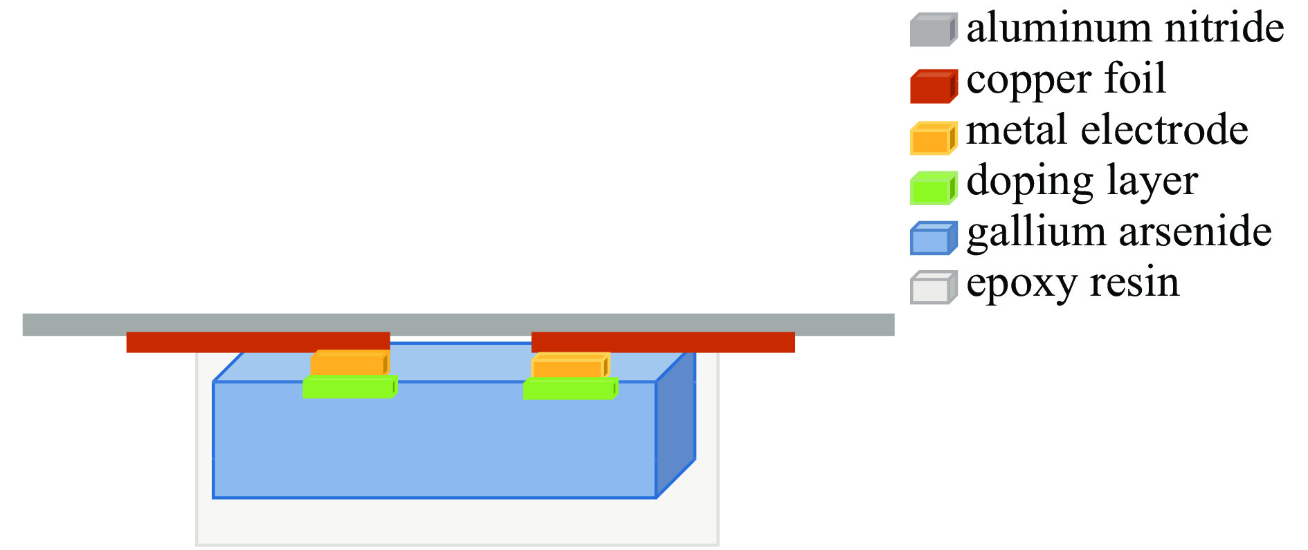
    Fig. 1. Structural schematic diagram of GaAs photoconductive switch
    Confocal response curves with different annular pupils
    Fig. 2. Confocal response curves with different annular pupils
    Current value of photoconductive switch under different bias voltage and minimum on-resistance value of photoconductive switch
    Fig. 3. Current value of photoconductive switch under different bias voltage and minimum on-resistance value of photoconductive switch
    Current value of photoconductive switch at different triggering energies and minimum on-resistance value of photoconductive switch
    Fig. 4. Current value of photoconductive switch at different triggering energies and minimum on-resistance value of photoconductive switch
    Current value of photoconductive at different triggering number
    Fig. 5. Current value of photoconductive at different triggering number
    Analysis of damaged surface morphology of switches
    Fig. 6. Analysis of damaged surface morphology of switches
    Diagram of damage between two electrodes of switch
    Fig. 7. Diagram of damage between two electrodes of switch
    Damage caused by thermal stress
    Fig. 8. Damage caused by thermal stress
    3-D effect map of damage layer
    Fig. 9. 3-D effect map of damage layer
    Huiru Sha, Longfei Xiao, Chongbiao Luan, Zhuoyun Feng, Yangfan Li, Xun Sun, Xiaobo Hu, Xiangang Xu. Damage morphology of GaAs photoconductive switch[J]. High Power Laser and Particle Beams, 2022, 34(9): 095018
    Download Citation