• Photonics Research
  • Vol. 7, Issue 3, 325 (2019)
Qianyi Mu1, Fei Fan1、2、3、*, Sai Chen4, Shitong Xu1, Chuanzhong Xiong1, Xin Zhang1, Xianghui Wang1, and Shengjiang Chang1、2、5
Author Affiliations
  • 1Institute of Modern Optics, Nankai University, Tianjin 300350, China
  • 2Tianjin Key Laboratory of Optoelectronic Sensor and Sensing Network Technology, Tianjin 300350, China
  • 3State Key Laboratory of Applied Optics, Changchun Institute of Optics, Fine Mechanics and Physics, Chinese Academy of Sciences, Changchun 130033, China
  • 4Nanophotonics and Optoelectronics Research Center, Qian Xuesen Laboratory of Space Technology, China Academy of Space Technology, Beijing 100094, China
  • 5e-mail: sjchang@nankai.edu.cn
  • show less
    DOI: 10.1364/PRJ.7.000325 Cite this Article Set citation alerts
    Qianyi Mu, Fei Fan, Sai Chen, Shitong Xu, Chuanzhong Xiong, Xin Zhang, Xianghui Wang, Shengjiang Chang. Tunable magneto-optical polarization device for terahertz waves based on InSb and its plasmonic structure[J]. Photonics Research, 2019, 7(3): 325 Copy Citation Text show less
    (a) Simulative carrier density of InSb at different temperatures; maps of the real part of (b) εL and (c) εR of longitudinally magnetized InSb in the THz regime under different magnetic fields from 0 T to 0.2 T; maps of theoretical transmittance (d) IL and (e) IR of longitudinally magnetized InSb in the THz regime under different magnetic fields from 0 T to 0.2 T; (f) map of the theoretical transmittance difference between the LCP and the RCP (IL−IR).
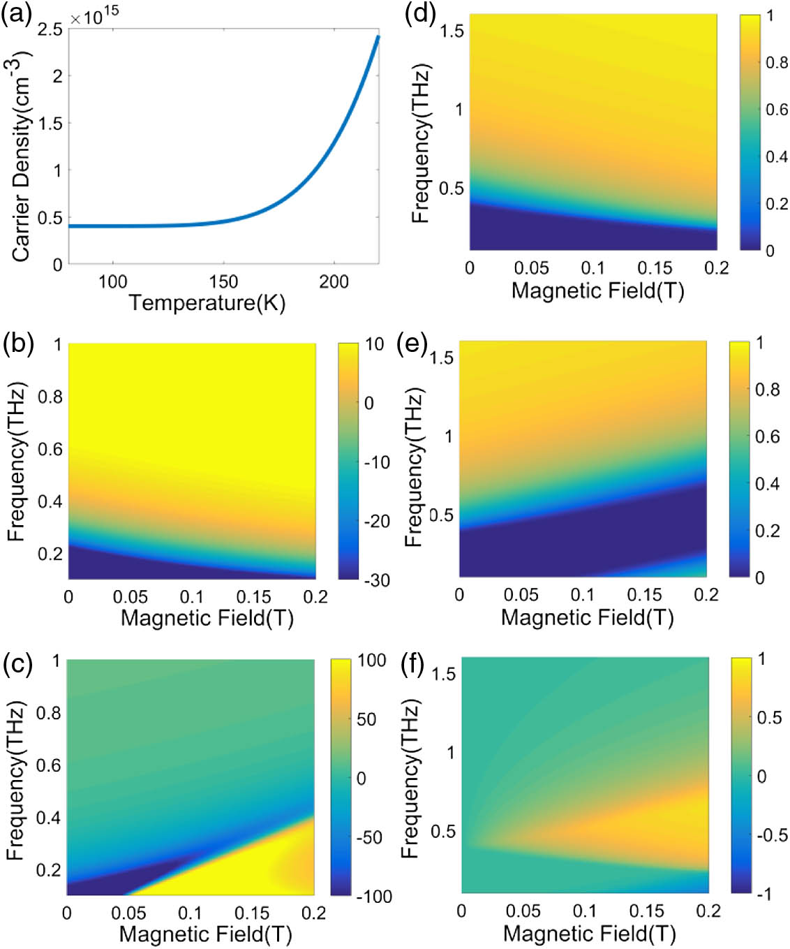
    Fig. 1. (a) Simulative carrier density of InSb at different temperatures; maps of the real part of (b) εL and (c) εR of longitudinally magnetized InSb in the THz regime under different magnetic fields from 0 T to 0.2 T; maps of theoretical transmittance (d) IL and (e) IR of longitudinally magnetized InSb in the THz regime under different magnetic fields from 0 T to 0.2 T; (f) map of the theoretical transmittance difference between the LCP and the RCP (ILIR).
    (a) Schematic diagram of experimental THz-MOS system; (b) photo of the experimental equipment.
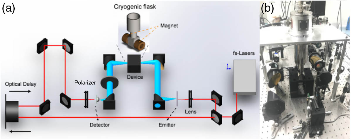
    Fig. 2. (a) Schematic diagram of experimental THz-MOS system; (b) photo of the experimental equipment.
    Experimental and simulated results of InSb with different temperatures: (a) measured THz time domain pulses; (b) experimental intensity transmission expressed in dB; (c) simulated carrier density N and cutting frequency fc; (d) simulated transmission.
    Fig. 3. Experimental and simulated results of InSb with different temperatures: (a) measured THz time domain pulses; (b) experimental intensity transmission expressed in dB; (c) simulated carrier density N and cutting frequency fc; (d) simulated transmission.
    Experimental results of InSb under magnetic field: (a) schematic diagram of the experimental configuration; (b) experimental time domain pulses in two orthogonal directions under magnetic fields of 150 mT and 0 mT; (c) experimental transmission of LCP and RCP components; (d) experimental Faraday rotation angles under different magnetic fields.
    Fig. 4. Experimental results of InSb under magnetic field: (a) schematic diagram of the experimental configuration; (b) experimental time domain pulses in two orthogonal directions under magnetic fields of 150 mT and 0 mT; (c) experimental transmission of LCP and RCP components; (d) experimental Faraday rotation angles under different magnetic fields.
    Polarization state vectors of the transmitted THz wave through InSb when the input wave is an LP light: polarization state at (a) 0.7 THz and (b) 1.1 THz under different magnetic fields; polarization state under (c) 0.13 T and (d) 0.17 T at different frequencies.
    Fig. 5. Polarization state vectors of the transmitted THz wave through InSb when the input wave is an LP light: polarization state at (a) 0.7 THz and (b) 1.1 THz under different magnetic fields; polarization state under (c) 0.13 T and (d) 0.17 T at different frequencies.
    (a) 3D schematic diagram of the InSb plasmonics in the experimental configuration; microscope image of grating 1 and grating 2; (b) side view of InSb plasmonics.
    Fig. 6. (a) 3D schematic diagram of the InSb plasmonics in the experimental configuration; microscope image of grating 1 and grating 2; (b) side view of InSb plasmonics.
    Experimental results of the InSb plasmonics: (a) measured y-LP THz pulses under different magnetic fields; (b) THz pulses under forward and backward magnetic fields of 150 mT; (c) amplitude transmission spectra under different magnetic fields; (d) spectra of the extinction ratio.
    Fig. 7. Experimental results of the InSb plasmonics: (a) measured y-LP THz pulses under different magnetic fields; (b) THz pulses under forward and backward magnetic fields of 150 mT; (c) amplitude transmission spectra under different magnetic fields; (d) spectra of the extinction ratio.
    Qianyi Mu, Fei Fan, Sai Chen, Shitong Xu, Chuanzhong Xiong, Xin Zhang, Xianghui Wang, Shengjiang Chang. Tunable magneto-optical polarization device for terahertz waves based on InSb and its plasmonic structure[J]. Photonics Research, 2019, 7(3): 325
    Download Citation