Dongwang YANG, Tingting LUO, Xianli SU, Jinsong WU, Xinfeng TANG. Unveiling the Intrinsic Low Thermal Conductivity of BiAgSeS through Entropy Engineering in SHS Kinetic Process[J]. Journal of Inorganic Materials, 2021, 36(9): 991
Copy Citation Text
It is of great significance to find the ultra-rapid preparation technology of materials and realize the optimization of electroacoustic transport properties in the research of thermoelectric materials. In this study, BiAgSeS compounds were successfully prepared by self-propagating high temperature synthesis (SHS), of which the kinetic process was systematically studied. It is found that the melting of Bi is the key to activate and initiate SHS reaction. In addition, the high concentrations of nano- and atomic-scale strain field regions, and screw dislocations produced in the non-equilibrium SHS process provide an everlasting step source for material growth and make the grains possess the layered structure. In the process of material densification, the step source continues to play a role in dominating grain growth, and thus leaving nanopores at the grain boundary. Because of these defects, compared with samples via melting-quenching (MQ) combined with plasma activated sintering (PAS), the SHS+PAS samples can slightly increase the electrical conductivity and significantly reduce the lattice thermal conductivity by ~6%. Finally, the thermoelectric properties are optimized, and the ZT is improved in the whole temperature range with the maximum value of 0.5 obtained at 773 K.
Thermoelectric (TE) materials can realize the direct conversion between heat and electrical energy without rotating parts or greenhouse emissions, thereby ensuring an important role in our global solution package of renewable energy[1,2,3]. The TE performance of a material is determined by figure of merit value ZT, i.e. ZT=α2σT/ (κel+κlat), where α, σ, κel, κlat, and T are the Seebeck coefficient, electrical conductivity, electric thermal conductivity, lattice thermal conductivity and the absolute temperature, respectively[1]. According to the above formula, ZT could be improved through either enhancing the power factor (α2σ), lowering the lattice thermal conductivity (κlat) or both at the same time[4,5,6].
Recently, entropy engineering has been employed to improve TE performance through a synergy of band structure engineering and multiscale hierarchical microstructures[7,8,9]. The entropy engineering stems from the design of high entropy alloy (HEA) in the field of metal[10]. HEAs typically refer to the solid solutions in which five or more principal metal elements, each in 5%-35% molar ratio, occupy at the same crystallographic site[11,12]. HEAs have four striking effects: (1) due to the high mixing entropy effect in thermodynamics, materials tend to form crystals with high symmetry such as body-centered-cubic (bcc) or face-centered-cubic (fcc) lattice; (2) hysteresis diffusion effect in dynamics, i.e. low diffusion kinetics facilitates in situ formation of nanoprecipitates; (3) severe lattice distortion effect in structure, i.e. extensive ionic mass and size mismatches result in reduced κph; and (4) “cocktail” effect in properties, i.e. complex constituents may lead to emerging phenomena[11,12].
In the field of medium and high temperature thermoelectric power generation, PbTe based compounds have the longest research history and exhibit excellent TE performance[13,14,15]. However, due to the toxicity of Pb and the scarcity of Te, its large-scale industrial application is greatly limited. As a substitute for PbTe based compounds, IB-VA-VIA2 (IB=Ag; VA=Sb, Bi; VIA=S, Se) rock salt compounds with double crystal cell structure have attracted extensive attention[16,17,18]. Theoretical and experimental studies show that the lone pair electrons in VA atom distort the lattice vibration and bring strong anharmonicity, which makes IB-VA-VIA2 compound exhibit intrinsic low thermal conductivity[16,17]. In addition, due to the disordered distribution of IB and VA elements in the cation site, the lattice thermal conductivity of IB-VA-VIA2 compound is further reduced, and the thermoelectric properties are optimized[19]. Recently, solution-grown nano- crystalline AgBiSe2 exhibits a high ZT of 1.5 at 700 K with reversible p-n-p conduction type switching[20]. Elemental metal and chalcogen melt grown ingots of p-type AgSb0.96Pb0.04Se2 and AgSb0.98Bi0.02Se2 achieve high ZT values of ~1.0 and ~1.15 at 680 K with superior electronic transport and ultralow thermal conductivity[16].
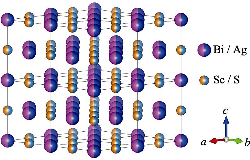
Combined with the design concept of high entropy alloy, if a variety of principal components are further introduced into the same anion site, that is, IB-VA-VIA(1)- VIA(2), then extremely fine microstructures may be generated in the material to further optimize the TE properties. Recently, BiAgSeS compound with intrinsic low thermal conductivity has been developed[21]. The crystalline structure of BiAgSeS is shown in Fig. 1, where Bi and Ag share the same cation site, Se and S share the same anion site, and both are in disordered states. Core effects of the HEA scheme and lone pair electrons effects from the VA atoms are expected to be reflected in this material at the same time.
Even though a variety of high-performance binary and ternary TE materials have been successfully prepared through self-propagating high-temperature synthesis (SHS) technology, research on quaternary and above compounds is still rare[22,23,24]. The non-equilibrium process with rapid heating and cooling rate produces rich microstructures, which may greatly scatter phonons and reduce the lattice thermal conductivity. In this study, BiAgSeS compound was successfully synthesized by the SHS method. The connection between SHS process and composition, structure and property of the synthesized materials was care-fully explored, which may shed light on the understanding of its intrinsic low thermal conductivity of BiAgSeS.
1 Experimental
Bi (99.999%), Ag (99.9%), Se (99.999%), and S (99.999%) powders were weighed according to stoichiometric ratio of BiAgSeS. The thoroughly mixed and hand ground powders were cold pressed into pellets at a pressure of 5 MPa for 5 min to achieve the reactant mixture pellet of ϕ15 mm. The pellet was then ignited by Joule heating a carbon foil under vacuum in a homemade SHS apparatus, in which the combustion temperature and wave propagation velocity could be measured. More synthesis details can be checked in our previous work[24].
Accordingly, stoichiometric amounts of high purity bismuth chunks (99.999%, Sinopharm Chemical Reagent Co., China), filamentary silver (99.999%, Sinopharm Chemical Reagent Co., China), selenium chunks (99.999%, Mount Emei semiconductor factory, China) and sulphur chunks (99.999%, Aladdin Chemical Reagent Co., China) were weighed and sealed in a silica tube under a pressure of 10-3 Pa. Subsequently, the tube was slowly heated up to 1123 K and maintained for 10 h, followed by quenching in saturated salt water.
The as-reacted product was hand ground and consolidated by plasma activated sintering (PAS) (PAS-III-Ed, Elenix, Japan) under a pressure of 30 MPa in vacuum at 890 K for 8 min. The resulting ϕ15 mm×3 mm cylindrical pellets were cut into different shapes for the TE property measurements.
2 Results and discussion
2.1 Single phased BiAgSeS by SHS technique
The high-speed camera recorded the SHS reaction of BiAgSeS. Fig. 2(a) shows different stages of the SHS process ignited at one end of the pellet. It is obvious that the combustion wave spreads rapidly. The height of the reactant pellet was 16.5 mm, and the reaction was completed in 14 s, so that the average spreading speed was about 1.18 mm/s. Fig. 2(b) displays the time dependent temperature profile of the SHS process of BiAgSeS recorded by the embedded thermocouple. The recorded temperature quickly increased and reached the maximum temperature of ~753 K within 8 s, and then decreased monotonically. Fig. 2(c) presents the X-ray diffraction (XRD) pattern of the final product. It can be seen that the diffraction peaks match well with the BiAgSeS standard card #98-010-4392. Indeed, the single phased BiAgSeS with fcc cubic structure forms after SHS, with the unit cell parameter of a=0.5734 nm.
Figure 2.Photographs (a) for different stages of the SHS reaction process, temperature profile (b) of the SHS reaction, and XRD pattern (c) of the SHS product
DSC was also used to “simulate” the SHS process in BiAgSeS, similar methodology as reported in our previous work[24]. Stoichiometric mixture of Bi, Ag, Se and S powder was cycled in a DSC between Tmin=293 K and Tmax=773 K, at a fastest possible heating rate of 85 K/min and a cooling rate of 50 K/min. As shown in Fig. 3(a), there are two endothermic peaks, Q1 (398 K) and Q2 (415 K), and one exothermic peak Q3 (549 K). To verify the nature of each peak, we varied Tmax=373, 400, 513 and 573 K that separate Q1, Q2 and Q3, and conducted the same heating-cooling DSC cycle. Fig. 3(b) shows the XRD pattern of the final product after cycling to different Tmax. In the powders after grinding, Ag reacts with Se to generate Ag2Se due to the strong dissociative adsorption reaction between Ag and Se[25]. At about 398 K, S melts as featured by an endothermic peak (Q1). At about 415 K, Se dissolves in S and generates eutectic compound S5Se4 (Q2). At 549 K, Bi melts and activates the system, which was featured by an exothermic peak (Q3). As the temperature further rises, all intermediate products, including Ag2Se, S5Se4, would react with liquid Bi to generate BiAgSeS compound. The following reaction scheme is suggested:
+Q1: S (s)=S (l)
+Q2: S (l)+Se (s)→S5Se4 (s)
-Q3: Bi(s)=Bi (l)
Bi (l)+Ag2Se (s)+S5Se4 (s) +... →BiAgSeS (s)
Where the “s” and “l” in the parenthesis stand for “solid” and “liquid”, the “+” and “-” in front of Q refer to endothermal and exothermal, respectively.
Figure 3.Heat flow (a) at a heating rate of 85 K/min and a cooling rate of 50 K/min, and XRD patterns (b) of the products with temperature cutting off at 373, 400, 513 and 573 K
To verify the reaction scheme, quenching experiment was performed to take a snap shot of the spatiotemporal process in SHS. Upon quenching the pellet in a stainless steel die[24], the combustion wave is extinguished as the heat is effectively shunted into the die. Fig. 4(a) displays the typical morphology of a quenched pellet, and the propagation direction of the combustion wave is shown by the pink arrow. The figure on the left from the front view shows a sharp boundary between the reaction zone and the unreacted zone, and the figure on the right from the top view presents four typical regions, which correspond to the raw material zone (1#), preheating zone (2#), reaction zone (3#) and the product zone (4#) of SHS process[26]. Each of these regions was examined using XRD and FESEM techniques. The XRD patterns from zone 1# to zone 4# are shown in Fig. 4(b), while the results of regional microstructure and composition analysis are presented in Fig. 4(c-f), respectively. In raw material zone 1#, the reaction mixture evenly distributes (Fig. 4(c)), some Se-S and Bi-Se compounds form in preheating zone 2# (Fig. 4(d)). The Se-S compound is paste-like, while the Bi-Se compound presents a layered structure with a size of about 5 mm. In the reaction zone 3#, BiAgSeS compounds were generated in large quantities (Fig. 4(e)). The surface of the crystal grains is smooth, with obvious traces of liquid flow and stepped growth, showing typical layer- to-layer growth characteristics from the solution. In the product zone 4#, all reactants transform into BiAgSeS (Fig. 4(b)), showing a nanolayered structure (Fig. 4(f)). However, in the process of crystal step growth, the extreme cooling rate of the SHS process causes the flat interface in the crystal growth to become unstable, which makes the steps gather to form a step beam, and the step beam becomes uneven and wavy when disturbed. In addition, the instability of the flat interface also forms edge faces, on which step beams grow (Fig. S1). The above microstructure analysis shows that the SHS process is a typical non-equilibrium process.
Figure 4.(a) Surface morphologies of the combustion wave quenching sample, (b) XRD patterns for typical regions, (c-f) FESEM images of microstructure and composition analysis from reactants to products (c) Mixture zone #1; (d) Preheating zone #2; (e) Reaction zone #3; (f) Product zone #4
Fig. 5(a-b) show the fracture surface morphology of BiAgSeS bulk samples after melt-quenching (MQ) and self-propagating high-temperature synthesis (SHS) combined with plasma activated sintering (PAS), respectively. Both samples are well compacted with relative densities higher than 98%, with the grain sizes of tens of microns. Compared with MQ+PAS samples, there are a large number of pores ranging from several to hundreds of nanometers in SHS+PAS samples. As shown in the locally enlarged illustration in Fig. 5 (b), these small pores are regular polygonal or circular, and locate at the grain boundary. This is because the step source on the crystal surface continues to grow during the densification process of PAS, and finally forms regular closed nanopores at the intersection of polycrystal boundaries.
Figure 5.Fracture surface morphologies of (a) MQ+PAS and (b) SHS+PAS BiAgSeS samples, and (c) secondary electron and (d) back scattering images of a polished surface of SHS+PAS sample
Fig. 5(c-d) depict the secondary electron images and back scattering images of a polished surface of the SHS+PAS BiAgSeS sample. The consistent composition contrast image documents the high phase purity of the final product, which can also be confirmed by its element surface distribution map (Fig. S2).
Figure S2.Elemental distributions on the surface of “SHS+PAS” sample
Fig. 6(a-b) show the high temperature XRD patterns of MQ+PAS and SHS+PAS BiAgSeS samples, respectively, from which it can be seen that both the low temperature and high temperature phase are cubic structures. This is due to the rapid cooling process during quenching or SHS and subsequent PAS process that the high temperature phases are preserved at room temperature. Moreover, temperature dependent XRD patterns clearly present the continuous structural transition from cubic to rhombohedral and then to cubic phases again in the heating stage. Similar to the isomorphous compound AgBiSe2, there was no obvious differentiation during the hexagonal- rhombohedral phase transition in the temperature-dependent XRD patterns. This is because atoms in BiAgSeS just slightly shift rather than rearrange during the hexagonal- rhombohedral phase transition process[27]. Obviously, the phase transition temperature range of the SHS+PAS sample (423-523 K) is slightly wider than that of the MQ+PAS sample (423-505 K). This may be because the SHS process has a faster cooling rate than the quenching process, and the finer defect structure makes atomic reconstruction more difficult during the phase transition process, which is consistent with the DSC heat flow curve (Fig. 7). It can be seen that the endothermic and exothermic peaks appear near 500 K in the heating stage and 453 K in the cooling stage, respectively, corresponding to the reversible phase transition in BiAgSeS. While the endothermic peak of about 540 K may be closely related to the fact that the second phase rich in Bi (melting point of 544 K) dissolved into the substrate. Interestingly, the broad endothermic peak around 500 K is asymmetry, which is probably a combination of cubic (low temperature metastable phase)-rhombohedral and rhombohedral- cubic (high temperature stable phase) structure transitions. Moreover, compared with the MQ sample, the SHS sample starts the phase transition earlier and has a wider temperature range, indicating that it is easy to trigger but difficult to complete the phase change for the finer microstructure. This is also consistent with the high temperature XRD results.
Figure 6.High temperature XRD patterns of (a) MQ+PAS and (b) SHS+PAS BiAgSeS bulk materials
Fig. 8(a) shows a low resolution TEM image of SHS+ PAS sample, which shows that there is a high concentration of nanoscale distortion region inside the sample. Fig. 8(b) shows the corresponding high resolution TEM image of SHS+PAS sample containing high concentration atomic scale stress distortion and defect regions. In order to observe the defects more clearly, the HRTEM image of the defect area is shown in Fig. 8(c, e), while Fig. 8(d, f) are the enlarged views of the yellow rectangles marked in Fig. 8(c, e), respectively.
Figure 8.Microstructures in BiAgSeS(a) Low-magnification TEM image revealing highly nanoscale distorted regions; (b) HRTEM image exhibiting highly atomic scale distortions; (c, e) HRTEM images depicting highly density of defects, including screw dislocation and strain-field domains; (d, e) Enlarged views of yellow marked regions in (c, e)
It can be seen that the crystal plane spacing of 0.21 and 0.28 nm in the matrix corresponds to the (022) and (002) crystal planes, respectively, which is consistent with the standard PDF card of BiAgSeS compound. There are a large number of strain field regions and screw dislocations in the SHS+PAS sample. It is known that these atomic and nanoscale defects can be generated in the non- equilibrium process of SHS and provide a step source for the material growth and densification. Here, the HRTEM observation shows that atomic and nanoscale defects retain inside the grains and nanopores at the boundary. These rich microstructures inevitably have an important impact on TE properties.
2.4 Thermoelectric properties
Fig. 9 presents the TE properties as a function of temperature for MQ+PAS and SHS+PAS BiAgSeS samples. The electrical conductivity increases with temperature (Fig. 9(a)), and the Seebeck coefficient decreases accordingly (Fig. 9(b)), which is a typical semiconductor transmission mechanism. Due to the high concentration defects produced by the non-equilibrium SHS process, the room temperature carrier concentration of SHS+PAS sample (6.68×1018 cm-3) is slightly higher than that of MQ+PAS sample (5.61×1018 cm-3), which ultimately makes the electrical conductivity of SHS+PAS sample slightly higher than that of MQ+PAS sample. The power factor increases significantly with temperature, reaching 3.6 and 3.7 mW·cm-1·K-2 for MQ+PAS and SHS+PAS sample at 773 K, respectively (Fig. 9(c)).
Figure 9.Thermoelectric performance of BiAgSeS samples(a) Electrical conductivity; (b) Seebeck coefficient; (c) Power factor; (d) Total thermal conductivity; (e) Lattice thermal conductivity; (f) Figure of merit ZT
The total thermal conductivity decreases first and then increases with temperature rising (Fig. 9(d)). Inflexion points appear at about 480 and 523 K, corresponding to the cubic (low temperature metastable phase)-rhombohedral and rhombohedral-cubic (high temperature stable phase) phase transitions, which are consistent with the DSC results. According to the Wiedemann-Franz relation, κel=LσT, where the Lorenz constant L can be obtained by combining the Seebeck coefficient and Hall coefficients and assuming a single band of carriers dominated by acoustic phonon scattering. The temperature dependent lattice thermal conductivity κL calculated by directly subtracting the electronic thermal conductivity κel from the total thermal conductivity κtot is displayed in Fig. 9(e). The lattice thermal conductivity κL of the two BiAgSeS samples are both lower than 0.7 W·m-1·K-1 in the whole temperature range of 300-773 K. Similar to AgBiSe2, we speculate that the extreme low lattice thermal conductivity in BiAgSeS system comes from: (1) the lone pair electrons in trivalent Bi possibly lead to serious asymmetric electron cloud density contributing to strong anharmonic disturbance to lattice vibration[16]; (2) high entropy effect caused by the disorder of Bi/Ag in cation sites and Se/S in anion sites strongly scatters phonons. Moreover, the κL of the SHS+ PAS sample is about 6% lower than that of MQ+PAS sample in the entire temperature range, which obviously originates from the exquisite microstructure inside. A large number of atomic and nano-scale strain field regions and pores induced by screw dislocations act as scattering centers of short- and medium-wavelength phonons, thus lead to much reduced phonon mean free path in the SHS+PAS BiAgSeS sample.
Finally, the slightly improved power factor combined with the greatly reduced lattice thermal conductivity optimized the thermoelectric properties of the SHS+PAS BiAgSeS sample. The figure of merit ZT value of the SHS+PAS BiAgSeS sample is higher than that of MQ+ PAS BiAgSeS sample in the entire temperature range (300- 773 K), and the maximum value reaches 0.5 at 773 K (Fig. 9(f)).
3 Conclusion
In this study, we successfully prepared BiAgSeS compound using self-propagating high-temperature synthesis technology and systematically studied the SHS kinetics process. It is found that the melting of Bi is the key to activate and trigger the SHS reaction. In addition, the high concentration of nano- and atomic-scale strain field regions, and screw dislocations produced in the non-equilibrium SHS process provide everlasting step sources for material growth, making the crystal grain a layered structure. In the process of material densification, the step source continues to play a role in leading the growth of crystal grains, and thus leaving regular shaped closed-nanopores at the grain boundaries. Compared with the MQ+PAS sample, it is precisely due to the existence of these defects that the SHS+PAS sample slightly improves the electrical conductivity, and remarkably reduces the lattice thermal conductivity by ~6%, and improves the TE performance. The ZT values in the whole temperature region is improved, and the maximum value of 0.5 is obtained at 773 K.
Supporting materials
Supporting materials related to this article can be found at https://doi.org/10.15541/jim20200698.
Supporting information:
Unveiling the Intrinsic Low Thermal Conductivity of BiAgSeS through Entropy Engineering in SHS Kinetic Process
YANG Dongwang1, LUO Tingting1,2, SU Xianli1, WU Jinsong1,2, TANG Xinfeng1
(1. State Key Laboratory of Advanced Technology for Materials Synthesis and Processing, Wuhan University of Technology, Wuhan 430070, China; 2. Nanostructure Research Center, Wuhan University of Technology, Wuhan 430070, China)
Measurement details:
Electrical Transport Properties. The electrical conductivity and Seebeck coefficient were measured on bar-shaped samples (3 mm×3 mm×11 mm) and conducted on an ULVAC-RIKO ZEM-3 (Ulvac®, Japan) instrument under a helium atmosphere from 300 to 773 K. The Hall coefficient (RH) at 300 K, was measured using a 5-wire configuration on a Physical Properties Measurement System (PPMS-9, Quantum Design®, USA) with the magnetic field strength sweeping between +/-1.0 T. The effective carrier concentration (nH) was calculated by the formulas: nH=1/eRH, with e being the electron charge.
Thermal Conductivity. The thermal conductivity was calculated using the relation κ = D·Cp·r, where the thermal diffusivity D was measured on a LFA457 (Netzsch®, Germany) laser flash apparatus. Thermal diffusivity (D) measurements were performed on square-shaped samples (8 mm×8 mm×1.5 mm). High temperature specific heat capacity Cp (300-773 K) was determined by a Differential Scanning Calorimetry (DSC) apparatus (Q20, Thermal Analysis®, USA). The packing density r of the sample was measured by the Archimedes method.
X-ray Diffraction and Microscopy. Phase purity of all samples was inspected by X-ray powder diffraction (Empyrean, Cu kα line, PANalytical®, Holland). Images of freshly fractured surfaces were taken by field emission scanning electron microscopy (FESEM) (SU8000, Hitachi®, Japan) with energy-dispersive X-ray spectroscopy (EDS) (XFlash6160, BRUKER®, Germany). Secondary electron images and back scattering images were taken by electron probe microanalysis (EPMA) (JXA-8100, JEOL®, Japan). Fine morphology was characterized by high-resolution transmission electron microscopy (HRTEM) (JEM- 2100F, JEOL, Japan).
References
[1] M ROWE D. CRC Handbook of Thermoelectrics(1995).
[11] N SENKOV O, D MILLER J, B MIRACLE D et al. Accelerated exploration of multi-principal element alloys with solid solution phases. Nature Communications, 6, 1-10(2015).
[14] Y PEI, A LALONDE, S IWANAGA et al. High thermoelectric figure of merit in heavy hole dominated PbTe. Energy & Environmental Science, 4, 2085-2089(2011).
[16] N GUIN S, A CHATTERJEE, S NEGI D et al. High thermoelectric performance in tellurium free p-type AgSbSe2. Energy & Environmental Science, 6, 2603-2608(2013).
[21] L PEI Y, H WU, J SUI et al. High thermoelectric performance in n-type BiAgSeS due to intrinsically low thermal conductivity. Energy & Environmental Science, 6, 1750-1755(2013).
[23] T HU, D YANG, X SU et al. Interpreting the combustion process for high-performance ZrNiSn thermoelectric materials. ACS Applied Materials & Interfaces, 10, 864-872(2017).