
Yuhao Guo, Zeinab Jafari, Lijuan Xu, Changjing Bao, Peicheng Liao, Guifang Li, Anuradha M. Agarwal, Lionel C. Kimerling, Jurgen Michel, Alan E. Willner, Lin Zhang. Ultra-flat dispersion in an integrated waveguide with five and six zero-dispersion wavelengths for mid-infrared photonics[J]. Photonics Research, 2019, 7(11): 1279
- Photonics Research
- Vol. 7, Issue 11, 1279 (2019)
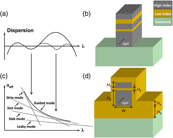
Fig. 1. Scheme for obtaining dispersion profile with more ZDWs. (a) The dispersion profile with another dip can introduce two more ZDWs. (b) The waveguide structure can generate the dispersion curve in (a), with one more slot layer added. (c) A slab beneath the waveguide core is introduced so that the guided mode extends to the slab more at a longer wavelength. (d) The proposed waveguide in this work.
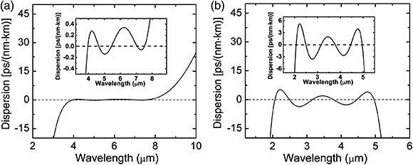
Fig. 2. Dispersion profiles of the guided mode over a wideband (a) for WG1 and (b) for WG2. Details of the dispersion are shown in the insets, individually.
Fig. 3. Mode evolution in this waveguide. (a) Optical field distributions of the quasi-fundamental-TM mode in WG1 at 4, 5, 6, 7, and 8 μm, respectively. (b) Normalized optical field overlaps of a fixed mode located at 6 μm with other modes at 4, 5, 7, and 8 μm.
Fig. 4. Dispersion profiles for WG2 with different structural parameters changed around the optimal values. (a) Different W H 1 H 2 H 3 H 4 H 5
Fig. 5. Dispersion profiles of the waveguides with the six structural parameters randomly changed within a range of ± 2.5 %
Fig. 6. Suggested waveguide fabrication process. (a) Thermal evaporation of GeSbS. (b) Spin-coating of photoresist. (c) UV exposure through photomask. (d) Photoresist development. (e) Thermal evaporation of GeSbSe, GeSbS, and GeSbSe. (f) Photoresist lift-off. (g) Thermal evaporation of GeSbS.
|
Table 1. Comparison of Dispersion-Flattened Waveguides in Recent Works
|
Table 2. Values of the Six Structural Parameters Randomly Changed within a Range of
|
Table 3. Values of the Six Structural Parameters Randomly Changed within a Range of

Set citation alerts for the article
Please enter your email address
© Copyright 2018-2021 | Chinese Laser Press. All Rights Reserved 沪ICP备15018463号-20