Yuhao Guo1, Zeinab Jafari1,2, Lijuan Xu1,3, Changjing Bao4..., Peicheng Liao4, Guifang Li5, Anuradha M. Agarwal6, Lionel C. Kimerling6, Jurgen Michel6, Alan E. Willner4 and Lin Zhang1,*|Show fewer author(s)
1Key Laboratory of Opto-electronic Information Technical Science of Ministry of Education and Key Laboratory of Integrated Opto-electronic Technologies and Devices in Tianjin, School of Precision Instruments and Opto-electronics Engineering, Tianjin University, Tianjin 300072, China
2School of Computer and Electrical Engineering, Shiraz University, Shiraz, Fars, Iran
3School of Electronic Engineering, Tianjin University of Technology and Education, Tianjin 300222, China
4Department of Electrical Engineering, University of Southern California, Los Angeles, California 90089, USA
5College of Optics and Photonics, CREOL and FPCE, University of Central Florida, Orlando, Florida 32816, USA
6Department of Materials Science and Engineering, Massachusetts Institute of Technology, Cambridge, Massachusetts 02139, USA
Yuhao Guo, Zeinab Jafari, Lijuan Xu, Changjing Bao, Peicheng Liao, Guifang Li, Anuradha M. Agarwal, Lionel C. Kimerling, Jurgen Michel, Alan E. Willner, Lin Zhang, "Ultra-flat dispersion in an integrated waveguide with five and six zero-dispersion wavelengths for mid-infrared photonics," Photonics Res. 7, 1279 (2019)
Copy Citation Text
We propose a new type of dispersion flattening technology, which can generate an ultra-flat group velocity dispersion profile with five and six zero-dispersion wavelengths (ZDWs). The dispersion value varies from to 0.35 ps/(nm·km) from 4 to 8 μm, which to the best of our knowledge is the flattest one reported so far, and the dispersion flatness is improved by more than an order of magnitude. We explain the principle of producing six ZDWs. Mode distribution in this waveguide is made stable over a wide bandwidth. General guidelines to systematically control the dispersion value, sign, and slope are provided, and one can achieve the desired dispersion by properly adjusting the structural parameters. Fabrication tolerance of this waveguide is also examined.
1. INTRODUCTION
Chromatic dispersion is one of fundamental properties of optical waveguides, which not only plays a critical role in shaping the temporal waveform of an optical pulse but also acts together with nonlinearity to affect pulse spectral evolution [1]. In nonlinear parametric interactions of continuous waves at different frequencies, dispersion is important in determining phase-matching conditions [1]. Thus, dispersion engineering has been widely used for parametric oscillation/amplification, supercontinuum, and frequency comb generation [2–4]. These technologies are indispensable to build broadband or octave-spanning optical sources for spectroscopy, imaging, frequency metrology, and communication.
In general, one needs to control many aspects of dispersion properties: (i) sign (i.e., normal or anomalous), (ii) value, (iii) dispersion slope, (iv) the number of ZDWs, (v) bandwidth where the dispersion of interest is obtained, and (vi) dispersion flatness (defined as flat-dispersion bandwidth divided by dispersion variation). Specific for broadband nonlinear applications [2–4], dispersion flattening is critical in achieving broadband phase-matching and high conversion efficiency. Dispersion engineering has been shown as a key enabler for two-octave frequency comb generation [5], three-octave supercontinuum generation [6], and octave-spanning amplification [7]. However, it is quite challenging to control multiple aspects of dispersion properties simultaneously in conventional optical waveguides. Dispersion naturally originates from materials and device structures and inevitably varies if one considers a large-enough bandwidth. In many cases, with multiple ZDWs, a dispersion profile tends to be bonded in a small variation range, and in this way the dispersion is made “flat”.
In recent years, dispersion engineering with multiple ZDWs has been proposed in various types of optical devices, such as photonic crystal fibers [8–12] and integrated waveguides [13–26]. In fibers, saddle-shaped dispersion curves with three and four ZDWs can be obtained by complicated geometry profiles, as a result of balanced waveguide dispersion and material dispersion. In integrated waveguides, a high-index contrast and tight mode confinement cause strong waveguide dispersion, which is usually dominant over material dispersion [13]. Therefore, dispersion flattening with multiple ZDWs is obtained by inducing additional waveguide dispersion from new structures to compensate for existent material/waveguide dispersion. As an example, strip/slot hybrid silicon waveguides over a large bandwidth have been proposed [14,15], and the general design guidelines of the nano-slot structures are also presented [17]. Different material combinations are proposed to achieve low and flat dispersion in single-slot and dual-slot waveguides [18,19,21,22]. Bilayer waveguides have been proposed to flatten dispersion with four ZDWs with the slot layer removed [24]. Compared to slot-assisted waveguides, these waveguides can be formed with a relatively low index contrast, making choices of materials more flexible and more fabrication-friendly.
Sign up for Photonics Research TOC. Get the latest issue of Photonics Research delivered right to you!Sign up now
Nevertheless, there are still some fundamental questions remaining unanswered. For example, how flat can a dispersion profile be? Is there an ultimate limit on the number of ZDWs? What is the maximum bandwidth for dispersion flattening?
These questions are important not only for deepening our understanding of dispersion engineering principle but also for practical applications. For example, middle infrared (mid-IR, from 2.5 to 20 μm, i.e., three octaves) is of particular interest recently [6,27–30], and on-chip mid-IR photonics [5,7,31–36] is intensively investigated. A research focus is to produce supercontinua [6,31–33] and broadband frequency combs [5,34,35] for spectroscopy/sensing and imaging applications [37,38]. In such a broad spectral region (three octaves), many conventional optical materials become absorptive, while some usable materials are mainly with high index [27], typically associated with strong waveguide dispersion. On the other hand, nonlinear photonics in deep mid-IR faces severe challenges [5], and these factors urge us to pursue dispersion flattening with multiple ZDWs as a promising technology for mid-IR applications. We list recent results in Table 1, including some works aiming to obtain low and flat dispersion in mid-IR using high-index materials such as Ge and [5,33,39,40] for a comparison of dispersion-flattened waveguides in terms of dispersion flatness and the number of ZDWs.
Year
Material
ZDWs
Dispersion [ps/(nm·km)]
λ (nm)
Δλ (nm)
Flatness (nm2·km/ps)
2011 [14]
Si3N4+SiO2a
4
−32to−11
1565–2100
535
25.48
2012 [15]
Si+SiO2
4
−22to+20
1435–2102
667
15.88
2012 [18]
Si+Si−nc
4
−24to+22
1527–2625
1098
23.87
2012 [19]
As2S3+SiO2
4
−3to+3
1685–2720
1035
172.50
2013 [21]
Si+Si−nc
4
−13to+14
1810–2655
845
31.30
2015 [22]
Si3N4+SiO2
4
−1to+1
1137–1949
682
341.00
2016 [24]
TiO2+Si3N4
4
−15.87to+11.34
1520–2320
800
29.40
2016 [24]
Si+GeSbSe
4
−4.7to+5.7
1660–3290
1630
156.73
2016 [39]
Si1−xGex
2
0to+14
3000–8000
5000
357.14
2017 [40]
Ge+Si
2
0to+59
3840–7920
4080
69.15
2018 [5]
Ge+Si
4
−16to+32
3500–10,000
6500
135.42
2018 [33]
Si0.6Ge0.4+Si
2
0to+19
4500–7700
3200
168.42
This work
GeSbSe+GeSbS
5
−0.15to+0.35
4000–8000
4000
8000.00
Si+Al2O3+Si3N4
6
−3.6to+5.1
2030–5030
3000
344.87
Table 1. Comparison of Dispersion-Flattened Waveguides in Recent Works
In this work, we propose a new type of integrated waveguide, in which different material combinations can be used to realize dispersion flattening. An ultra-low and flat dispersion profile can be obtained over an octave-spanning bandwidth in mid-IR, with a total variation of 0.5 ps/(nm·km), which to the best of our knowledge is the flattest one reported so far. More importantly, we show how to produce five or even six ZDWs in the proposed waveguides with different material combinations, which demonstrates unprecedented capability and versatility of dispersion engineering in integrated photonic waveguides.
2. DISPERSION FLATTENING PRINCIPLE
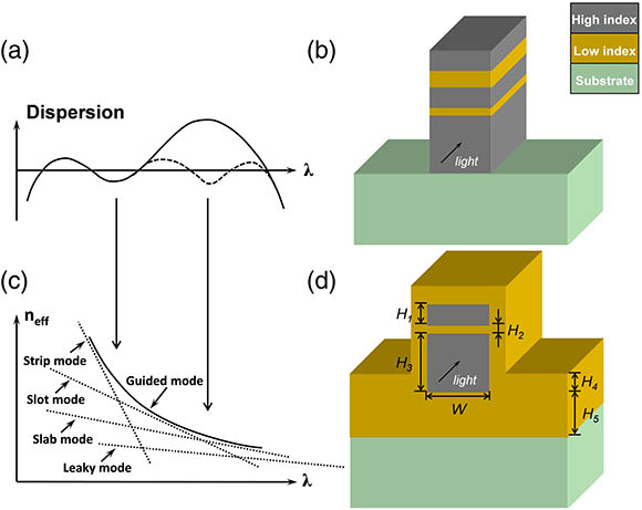
For dispersion tailoring with multiple ZDWs, a natural and fundamental question would be how many ZDWs a waveguide can have. If possible, producing more ZDWs, as shown in Fig. 1(a), not only deepens our understanding on the principle of dispersion engineering but can also significantly extend the low-dispersion bandwidth, which is highly desirable for broadband nonlinear applications [5–7]. Since a nano-scale slot has been successfully used for inducing normal dispersion in the middle of dispersion bandwidth and two more ZDWs [14,15], one may think of adding another slot layer to produce more than four ZDWs, as shown in Fig. 1(b). Note that, in this way, the second slot has to be designed for a longer wavelength, in order to introduce another dip in the dispersion profile in Fig. 1(a). By properly adjusting structural parameters, one may in principle obtain a dispersion profile with two more ZDWs, compared to the slot-assisted waveguides in Refs. [14,15].
Figure 1.Scheme for obtaining dispersion profile with more ZDWs. (a) The dispersion profile with another dip can introduce two more ZDWs. (b) The waveguide structure can generate the dispersion curve in (a), with one more slot layer added. (c) A slab beneath the waveguide core is introduced so that the guided mode extends to the slab more at a longer wavelength. (d) The proposed waveguide in this work.
However, there is an obvious drawback of this waveguide, i.e., the mode will be continuously lifted up as wavelength increases [15], which may result in a small optical field overlap between two modes that are spectrally far apart. Then, this causes a significant reduction in the effective nonlinear interaction over an octave-spanning bandwidth and a decrease in nonlinear conversion efficiency. Therefore, it is preferred to keep the guided mode stable in the vertical direction, while engineering a dispersion profile. To this end, we introduce a slab beneath the waveguide core so that the guided mode extends to the slab more at a longer wavelength, as shown in Fig. 1(c). Note that we also coat the waveguide core with a low-index layer. Without it, the mode can be dragged down to the slab quickly as wavelength increases. Finally, the proposed waveguide is presented in Fig. 1(d). At short wavelengths, the guided mode is tightly confined in the lower layer of the inner trilayer waveguide as in Refs. [14,15], simply like a strip mode. As wavelength increases, the first mode transition occurs within the inner trilayer part assisted by a slot layer [15], generating a saddle-shaped dispersion profile. At longer wavelengths, the guided mode extends into both the coat and the slab. The mode experiences the second transition as in Ref. [24], and in this process the inner trilayer part together with the coat, as a whole, can be regarded as the waveguide core, and the mode shifts from it toward the slab as in a bilayer waveguide proposed in Ref. [24], which forms the second saddle-shaped dispersion. Finally, a low and flat dispersion with two more ZDWs can be obtained by choosing an appropriate parameter set.
3. RESULTS OF DISPERSION ENGINEERING
A. Proposed Dispersion-Flattened Waveguides
The waveguide can be formed by different combinations of materials, and here we show two cases (WG1 and WG2). In WG1, the materials are (GeSbSe, ) and (GeSbS, ), and the substrate is . In WG2, the materials are Si (), (, slot), and (, coat and slab), and the substrate is air, which can be formed by partially wet-etching in an SOI wafer [41]. Different from WG1, the materials of the slot layer and the coat layer are not the same for WG2, which are and individually. All material dispersions are taken into account using Sellmeier equations [29,42–44]. We employ a full-vectorial mode solver to obtain the effective refractive index () of the fundamental quasi-TM mode. The chromatic dispersion of the guided mode is expressed by where is the wavelength, and is the speed of light in vacuum.
For WG1, the parameters of the structure are , , , , , and . Figure 2(a) shows the dispersion of the guided mode. An ultra-low and flat dispersion profile can be obtained from 4 to 8 μm wavelengths. As clearly seen from the inset, the dispersion varies from to 0.35 ps/(nm·km), with five ZDWs located at 3.98, 4.66, 5.42, 7.08, and 7.52 μm, respectively. We see from Table 1 that the dispersion flatness of this waveguide is quite high compared to previous works. Note that the anomalous dispersion at wavelengths beyond 8 μm is due to the material dispersion of substrate [43].
Figure 2.Dispersion profiles of the guided mode over a wideband (a) for WG1 and (b) for WG2. Details of the dispersion are shown in the insets, individually.
For WG2, the parameters of the structure are , , , , , and . For the slot, the dispersion of the guided mode is presented in Fig. 2(b), and a low and flat dispersion with a change from to 5.1 ps/(nm·km) can be obtained from 2.03 to 5.03 μm. Different from WG1, it is noted that there are six ZDWs generated by WG2, which are located at 2.12, 2.49 3.14, 3.78, 4.45, and 5.02 μm, respectively. In addition, the dispersion variation for WG2 is larger, due to a higher index contrast among waveguide materials [17]. Details of the dispersion profiles are shown in the insets of Fig. 2 individually for WG1 and WG2.
These two examples show flexibility of material choices in the proposed dispersion flattening technology. We note that, in terms of index contrast as a key parameter defined as refractive index ratio [17], WG1 and WG2 have quite different index ratios. Also, in WG2, high and low refractive indices cover a larger range than those in WG1. This means that one can effectively tailor dispersion for more than 4 ZDWs with material combinations from a wide range of optical materials. In other words, the proposed dispersion engineering technique can serve as general methodology, instead of being found out with a special trick.
B. Mode Evolution in This Waveguide
The mode evolution in the proposed waveguide is illustrated in Fig. 3(a). At short wavelengths, the guided mode is tightly confined in the high-index layer of the inner trilayer waveguide, simply like a strip mode. As wavelength increases, the mode extends more into the slot (first mode transition) [15], generating a saddle-shaped dispersion profile. At longer wavelengths, the guided mode extends further into the coat and slab layers. In this transition, the slab and the waveguide structure above the slab form a “bilayer” waveguide as in Ref. [24] and produce the second dispersion dip. Note that, to explain in principle, we differentiate the two mode transitions as wavelength increases, but the two processes cannot be clearly separated. In fact, the mode stays quite stable in the vertical direction, instead of moving up and then down. Figure 3(a) shows the optical field distributions of the guided mode in WG1 at 4, 5, 6, 7, and 8 μm. We can see that the mode is well centered in the lower GeSbSe layer as wavelength increases.
Figure 3.Mode evolution in this waveguide. (a) Optical field distributions of the quasi-fundamental-TM mode in WG1 at 4, 5, 6, 7, and 8 μm, respectively. (b) Normalized optical field overlaps of a fixed mode located at 6 μm with other modes at 4, 5, 7, and 8 μm.
For broadband or octave-spanning nonlinear applications, modal field overlap among far apart frequency components becomes an important issue, and low modal overlap can lead to a significant reduction of nonlinear conversion efficiency [45]. To verify the advantages of the proposed waveguide, we calculate the mode overlap factor [46] between different wavelengths for WG1. Here, we choose a mode located at 6 μm and obtain its mode overlap factors with other fundamental TM modes at 4, 5, 7, and 8 μm, as shown in Fig. 3(b), which are 0.9778, 0.9961, 0.9931, and 0.9780, respectively. This means that the influence of modal field mismatch is negligible in broadband nonlinear processes in the proposed waveguide.
Although flattened dispersion is needed in general for broadband nonlinear applications, a dispersion profile has to be optimized specifically for each application scenario [5–7]. The guidance for dispersion tailoring in the proposed waveguides to achieve the desired dispersion properties is presented in Fig. 4. Since WG2 has a dispersion profile not dominated by material dispersion at the long-wavelength end and also dispersion engineering is mainly about how to tailor waveguide dispersion, we take WG2 as an example to show how a dispersion profile can be shaped in different ways over a wavelength band more than one octave. We change each of the structural parameters around the values given for Fig. 2(b) by 1%–2% every time, while keeping the others fixed. As seen from Fig. 4(a), dispersion at long wavelengths is more sensitive to and becomes more anomalous as increases. Figure 4(b) shows that the dispersion profile rotates as we increase gradually, with a nearly zero value at around 3.5 μm, which is almost the center of the flat-dispersion band. Thus, one can modify the third-order dispersion, while keeping the average dispersion almost unchanged over a wide bandwidth. The influence of the slot layer on the total dispersion is illustrated in Fig. 4(c). In contrast with Fig. 4(b), dispersion at the central wavelength is more sensitive than at other wavelengths, producing a nearly symmetric dispersion profile over wide spectra as becomes larger. As we increase , the dispersion profile is entirely moved up without a dramatic change in its shape and slope, which means that we can obtain the same flat-dispersion bandwidth with different signs. Figure 4(e) shows that has increasingly more influence on dispersion after μ, due to the fact that more and more power extends to the coat layer as wavelength increases and the dispersion is changed to be normal with the increased . Figure 4(f) presents that the slope of dispersion can be slightly tailored by modifying , and dispersion is less sensitive to this parameter compared to others.
Figure 4.Dispersion profiles for WG2 with different structural parameters changed around the optimal values. (a) Different , (b) different , (c) different , (d) different , (e) different , and (f) different .
From above, it is outlined that a dispersion profile in the proposed waveguide can be rotated, as in Figs. 4(a), 4(b), 4(e), and 4(f), and moved up and down as in Fig. 4(d), while its shape can be modified as in Fig. 4(c). For a rotation of a dispersion profile, Figs. 4(a) and 4(e) represent a coarse tuning, and Fig. 4(f) shows a fine tuning, while Fig. 4(b) provides a different rotation center. It is important to emphasize that one may need to simultaneously vary more than one parameter to reach the goals of dispersion engineering listed in the introduction section. For example, by jointly varying and and keeping the others the same, one can make both the second-order and third-order dispersion nearly zero from 3 to 4 μm. Generally speaking, the flexibility of dispersion tailoring in the proposed waveguide provides us with a valuable and significantly extended parameter space for waveguide properties, allowing manipulation of ultrashort optical pulses over an ultrabroadband spectral range by precisely controlling the timing of intra-pulse frequency components. This would greatly enrich broadband nonlinear phenomena, beyond what have been proposed in Refs. [5–7].
4. ANALYSIS OF FABRICATION TOLERANCE
In order to examine the fabrication tolerance of the proposed waveguides, we randomly change the six structural parameters within a range of for both WG1 and WG2, which is repeated 10 times. We plot the obtained dispersion profiles in Fig. 5. The structural parameters are listed in Tables 2 and 3. As shown in Fig. 5(a), the overall dispersion variation for WG1 is smaller than 15 ps/(nm·km) for all 10 cases, and the dispersion slope has a negligible change over the low-dispersion bandwidth, meaning that dispersion of this waveguide is tolerant to the dimension variations in device fabrication. Compared to WG1, WG2 is a bit more sensitive to dimension variations and the overall dispersion variation is about /(nm·km).
Figure 5.Dispersion profiles of the waveguides with the six structural parameters randomly changed within a range of for 10 times to mimic the influence of fabrication errors (a) for WG1 and (b) for WG2.
A suggested fabrication process for the waveguide is shown in Fig. 6. We take WG1 as an example. First, using thermal evaporation, a blanket film of GeSbS is deposited on top of a wafer. Then, a negative lift-off photoresist is spin-coated with a thickness slightly greater than that required for the devices to be fabricated. Using a chrome-on-quartz photomask, a pattern is created in the negative photoresist by exposure with a contact aligner. The UV light crosslinks the photoresist so that, when the sample is immersed in a developer solution containing tetramethyl ammonium hydroxide (TMAH), the unexposed regions are washed away. This leaves a negative image of the ultimate pattern. Following lithography, three successive thermal evaporation steps are carried out to build a structure comprised of a thin layer of GeSbS sandwiched between two thicker layers of GeSbSe. As a final step, a thin layer of GeSbS is thermally evaporated to coat the devices. It is important to mention that waveguide sidewalls may not be maintained vertical after fabrication, and this can result in a change in the dispersion profile. However, it can be corrected by slightly tailoring other structural parameters.
Figure 6.Suggested waveguide fabrication process. (a) Thermal evaporation of GeSbS. (b) Spin-coating of photoresist. (c) UV exposure through photomask. (d) Photoresist development. (e) Thermal evaporation of GeSbSe, GeSbS, and GeSbSe. (f) Photoresist lift-off. (g) Thermal evaporation of GeSbS.
In conclusion, we propose a new dispersion-flattening technology that generates an ultra-flat dispersion profile with five or even six ZDWs. Two material combinations with different index contrasts are presented to realize dispersion flattening, exhibiting the universality of the proposed dispersion engineering scheme. A very small dispersion variation of 0.5 ps/(nm·km) can be obtained in the chalcogenide waveguide over a broad band more than one octave in the deep mid-IR. The dispersion flatness can be as large as , which is the highest to the best of our knowledge. The proposed silicon waveguide exhibits six ZDWs in a flattened dispersion profile, which has never been demonstrated in optical waveguides and fibers.
The dispersion-flattened waveguides in this work represent the unprecedented capability of dispersion engineering in high-index-contrast integrated photonics, which has not been shown in optical fibers. This proves that high-index-contrast waveguides are not only suitable for producing strong dispersion but are also feasible to enable ultra-small dispersion over a wide bandwidth. This greatly extends parameter space of dispersion engineering originating from optical fiber technologies. More importantly, generating five or even six ZDWs is expected to open an opportunity for exploring enriched nonlinear phenomena and mechanisms in broadband mid-IR photonics.
Acknowledgment
Acknowledgment. We acknowledge support by the Advanced Integrated Optoelectronics Facility at Tianjin University.
References
[1] G. P. Agrawal. Nonlinear Fiber Optics(2006).
[2] M. Marhic. Fiber Optical Parametric Amplifiers, Oscillators and Related Devices(2007).
[3] R. R. Alfano. The Supercontinuum Laser Source(1989).
[4] J. Ye, S. T. Cundiff. Femtosecond Optical Frequency Comb: Principle, Operation, and Applications(2004).
[25] A. D. Torre, M. Sinobad, B. Luther-Davis, P. Ma, S. Madden, S. Debbarma, K. Vu, D. J. Moss, A. Mitchell, J. Hartmann, J. Fedeli, C. Monat, C. Grillet. Tailoring the dispersion of a hybrid chalcogenide/silicon-germanium waveguide for mid-infrared supercontinuum generation. Conference on Lasers and Electro-Optics, FF2D.8(2019).
Yuhao Guo, Zeinab Jafari, Lijuan Xu, Changjing Bao, Peicheng Liao, Guifang Li, Anuradha M. Agarwal, Lionel C. Kimerling, Jurgen Michel, Alan E. Willner, Lin Zhang, "Ultra-flat dispersion in an integrated waveguide with five and six zero-dispersion wavelengths for mid-infrared photonics," Photonics Res. 7, 1279 (2019)