
Feng Zhou, Cacere Jelah Nieva, Dianyuan Fan, Shunbin Lu, Wei Ji. Superior optical Kerr effects induced by two-dimensional excitons[J]. Photonics Research, 2022, 10(3): 834
- Photonics Research
- Vol. 10, Issue 3, 834 (2022)
Abstract
1. INTRODUCTION
The optical Kerr effect (OKE) is one of the nonlinear optical (NLO) phenomena observed in dielectric or semiconducting materials, where the refractive index changes in response to intense laser light. The change of refractive index (or so-called nonlinear refractive index, ) leads to Kerr lensing [1] and phase modulation [2] of the laser light. By utilizing these characteristics, materials with the OKE have shown great potential for applications, such as all-optical switching, all-optical modulation, four wave mixing, optical parametric amplification, and laser mode-locking [3–8]. In the above-mentioned context, an ideal OKE material should possess large nonlinear refractive index at low optical power. In addition, a short response time is also crucial. Prior to this work, spectra of various 3D dielectrics and semiconductors have been experimentally measured [9–11] and theoretically verified via a two-parabolic band (TPB) model [12]. Such a theory provides a general guideline on predicting the magnitude of bulk semiconducting materials. However, 3D materials usually show either weak nonlinear refractive change or long response time even under illumination with strong optical fields. Such limitations therefore call for alternative strategies in order to obtain OKE materials for efficient all-optical devices.
One such strategy is to exploit excitonic effects of 2D materials (or so-called 2D excitons). The 2D exciton can be naturally formed by optical coupling excitonic transitions in layered materials where the spatial confinement and the reduced screening effect give rise to enhanced Coulomb interactions. Since the excitons are confined in a plane that is thinner than their Bohr radius in most 2D semiconductors [13–15], quantum confinement enhances the exciton binding energy [16] and alters materials’ optical properties [17]. In particular, the 2D exciton layered materials manifest strong and ultrafast light–matter coupling on nonlinear optical responses in the visible to the near-infrared spectra [18,19]. For instance, a single crystal of Ruddlesden–Popper perovskite (RPP) in the 2D structure has been reported to possess an dispersion with a remarkable resonant feature arising from the Pauli blocking [1] in one-photon-induced transitions to the lowest excitonic state [20], giving rise to considerable OKEs in the visible range. The temporal response for this OKE has been reported to be , which is attributed to either an exciton-exciton annihilation (EEA) effect or a radiative recombination process of the excitons [21–24]. Apart from the one-photon absorption, OKEs along with the two-photon absorption (2PA) have also been reported in 2D semiconducting materials, where the photon energy () of the incident light is far below the bandgap (), i.e., . It is noted that values of layered crystals of RPP, (), have shown more than an order of magnitude, as compared with a bulk semiconductor and the TPB model [25] at the excitation wavelength of 2.7 μm. The enhancement of the OKEs was demonstrated to arise from excitonic effects on the 2PA [26,27]. Upon the 2PA associated OKEs, “dark” excitons are created instantaneously and then relax through electron-electron interaction, which exhibits a fast temporal decay in transition metal dichalcogenide (TMD) monolayers and RPPs [23,27]. However, a theoretical guideline and systematic understanding on the OKE of 2D layered materials are still lacking.
In this paper, we develop a simple model on OKEs originated from 2D exciton-associated 2PA. By utilizing the second-order quantum perturbation theory for two-photon transitions among the energy states of 2D excitons and then performing the Kramers–Kronig (K-K) transformation, the nonlinear refractive index () is successfully derived over a broad range of light frequency with an assumption that only exciton is taken into consideration. The theoretically calculated results from our model are comparable with those reported experimental data for monolayer RPPs, TMDs, black phosphorus (BP), and hexagonal boron nitrides (h-BNs). Furthermore, our model explicitly shows that the dispersions of 2D semiconductors are dominated by exciton-resonant features, in particular, the resonance with the exciton; and the magnitudes are closely related to both its linewidth and energy level. The value of a 2D RPP is predicted to be , which is four orders of magnitude more than those of bulk semiconductors () [10], demonstrating the superior OKEs induced by 2D excitons and implying a narrow refractive index-near-zero region for intense laser light. Last, we evaluate the figures-of-merit (FOMs) of the OKEs for these 2D semiconductors, which proves them to be of great potential for all-optical excitonic devices.
Sign up for Photonics Research TOC. Get the latest issue of Photonics Research delivered right to you!Sign up now
2. THEORY
The nonlinear refractive index () intrinsically accompanied by the 2PA coefficient () is governed by the K-K relation [1]. In the present context, we write it in the form
For a novel K-K transformation, two distinct photon energies for 2PA are needed, i.e., the “cause” and the integration variable in Eq. (1). Here, we consider a special case for the degenerate 2PA, in which the photon energies and are equivalent. The degenerate in the case of exciton-resonant 2PA of 2D semiconductors is schematized by Fig. 1 and has been calculated based on a second-order, time-dependent, quantum-mechanical perturbation theory [28,29]. Here, we simplify the expression of degenerate further, and the detailed simplification can be found in the appendix. The simplified expression is as follows:
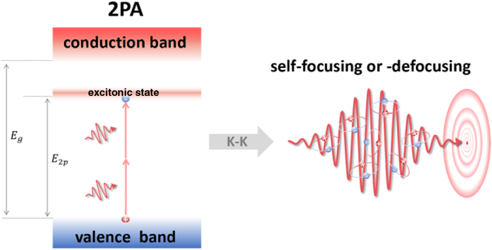
Figure 1.Schematic of the optical Kerr effect (self-focusing or -defocusing) induced by 2PA resonant with the exciton energy (
By substituting Eq. (2) into Eq. (1), the dispersion is derived to be
Because the equivalence of and would lead to the integral of with divergences, a substitution of with and a numerical summation were made for an approximate integral of over the 2PA range (). With further simplifications, see the details in Appendix B; we obtain a semiempirical expression as
3. RESULTS AND DISCUSSION
Note that Eq. (5) interprets the normalized -dispersion. As shown by the pink area in Fig. 2, the normalized values with being in the range from 0.05 to 0.15 exhibit a central-symmetrical dispersion with respect to . For , the normalized values vary from the positive to the negative dramatically, indicating that the OKE would be on (or near) resonance with . Otherwise, the normalized values can be regarded as the off-resonant ones and are nearly independent on or .
![]()
Figure 2.Comparison of the normalized
To validate our model, the calculated dispersions are normalized and compared with experimental data of monolayer (or few-layer) TMDs, RPPs, h-BN, and BP [25,30–34], where the values of are obtained from Table 3 in Appendix A. In the off-resonance region, our model is in agreement with the experimental data within an order of magnitude for RPP () in polycrystalline structures (at 2.7 μm) [25] and h-BN (at 1.064 μm) [33]. The experimental data of RPP () powders are less than the prediction of Eq. (4). It is anticipated that surface states and/or surface scattering from the crystallites may hinder its intrinsic NLO properties of the 2D crystals. The normalized value of BP [34] is at , which is comparable with the magnitude predicted by Eq. (4), but it is not shown because it is beyond the scale of the axis in Fig. 2.
In the near-resonance region, there is a large discrepancy with the experimental data of monolayer (or few-layer) TMDs [30–32], which is attributed to the spin-split-off excitonic states. Experimental evidence has shown monolayer TMDs with the spin-orbital splitting possess a pair of generated excitons (as either the A-exciton or B-exciton [35]) transitioning at the and valley in the momentum space with broken inversion symmetry. This gives rise to a unique valley degree of freedom in the dispersions that can directly couple to the helicity of excitation photons [17]. Under two-photon excitation, it is necessary to consider the two excitons; hence, as detailed in Appendix A, the dispersion is modified to be
Figure 3 shows good agreement between Eq. (6) and the experimental data. and result in two peaks in the near-resonance region, indicating that the spin-split-off energy of excitons should play a significant role in the OKE of monolayer TMD materials. Furthermore, the B-exciton with a higher energy level from the spin-orbital splitting leads to a broadened and blueshift of the resonance of the individual dispersion, in comparing the blue curves to the red ones in Fig. 3. This is attributed to higher energy levels of B-excitons, which exhibit larger linewidths of NLO resonance. The spin-splitting effect makes a great variation of overall values as displayed by the purple curves.
![]()
Figure 3.Normalized
Figure 4 compares calculated magnitudes from Eq. (4) or Eq. (6) with the TPB model. It is interesting to note that the maximal values by Eq. (4) or Eq. (6) are in the range from to , which are greater than the TPB model results by at least one order of magnitude. This indicates the 2D excitonic effects greatly enhance the OKE in 2D cases when compared with their bulk counterparts. As derived in Eqs. (4) and (6), the calculated values are proportional to , implying 2D materials possessing the higher density of excitons and/or the larger effective Bohr radius would exhibit greater OKE along with degenerate 2PA in many ways analogous to plasma screening effects [36]. As a result, RPP () is predicted to show the largest peak value of among the 10 materials. The calculated values are of the same order of magnitude as the multilayer graphene at an excitation wavelength in the near-infrared [37]. As compared with the experimental data of monolayer (or few-layer) TMDs in thin films, or dispersion [31,38–41], the measured absolute values are greater than from Eq. (6) [38,40,41]; also see Table 4 in Appendix C. One reason for the discrepancy is that the presence of a large number of defects/impurities in these films would give extra transitions in either 2PA or saturable absorption (SA) processes and, thus, enhance the measured nonlinearities. It is also noted that the absolute values from our model are one order of magnitude larger than the reported results of dispersion [31] and nanosheets [39], where light scattering in those amorphous samples may screen a refractive index change arising from the 2D nature of excitons.
![]()
Figure 4.Calculated
With the effects of 2D excitons, further enhancement of the OKE is predicted at lower temperature. As derived from Eq. (4) or (6), values on resonance are inversely proportional to the square of the linewidth () of 2D exciton, which would narrow down (as ) for RPPs, with temperature decreasing to [42]. The temperature dependence of the OKE could enlarge values at peak (or valley) by one order of magnitude [see an example of dispersion of RPP () in Fig. 5(a)]. The value of RPP () is predicted to be at 7 K, which would lead to a change in the refractive index of 3 (i.e., around 150% of the linear refractive index) in the case of . This would give rise to a narrow refractive index-near-zero region of intense laser light when it is on resonance with 2D exciton. In the off-resonance region, our calculated values are nearly independent of or the linewidth (). The scaled values explicitly show an dependence, which gives a variation by two orders of magnitude for 2D semiconducting materials with ranging from 1 to 10 eV. This variation is clearly illustrated in Fig. 5(b).
![]()
Figure 5.(a) Calculated
Indeed, in our model, the absolute magnitude of the nonlinear refractive index is enhanced through two-photon transitions, when the photon energy approaches . Such a resonant enhancement of is basically accompanied by absorption losses, commonly given by , where is the linear absorption coefficient. The OKE efficiency/transparency trade-off () at a specific wavelength is therefore of importance to the assessment of a material for all-optical switching devices. The material requirements are as follows: and [43,44]. Table 1 lists the FOMs for selected materials operated at room temperature, , and . Among them, RPP () is the best: its is predicted to be as large as with both and . Compared with multilayer graphene, Si, and GaAs, RPP () performs even better, as its nonlinear refractive index is enhanced by two orders of magnitude, while is comparable [45,46]. Though RPPs () exhibit better (), indicating less 2PA losses, the values are less than 1 [29]. Note that the required light irradiance () would be high. To reduce it, 2D materials in microcavities or photonic structures should be considered. For example, one may integrate 2D materials on clad nanophotonic cavities, such as ring and disk resonators, to increase the effective path length for light–matter interaction [47]. Arbitrary vertical heterostructures such as intentionally designed sequences of graphene, h-BN, and TMD monolayers (or 2D perovskites) [48,49] would give also rise to higher 2D-exciton density in order to reduce the operating light intensity. Nonlinear Coefficients and FOMs of Materials at 1550 nmMaterial Ref. 2D RPP ( 105.5 96.3 1.02 0.14 This work 2D RPP ( 22.9 9.9 0.27 0.07 This work 2D RPP ( 7.2 1.6 0.12 0.03 This work 2D RPP ( 1.3 0.3 0.03 0.04 This work 2D 1.5 5.6 0.008 0.56 This work 2D 19.1 212.5 0.07 1.72 This work 2D 2.7 7.7 0.02 0.45 This work 2D 15.8 79.1 0.06 0.78 This work Multilayer graphene −800 900 0.20 1.40 [ 0.045 0.79 – 0.37 [ GaAs 0.16 10.2 – 0.10 [ GaAs/AlAs superlattice 0.15 1.5 – 0.87 [ Conjugated 3,3’-bipyridine derivative 0.0046 [
4. CONCLUSION
In summary, based on the K-K transformation of exciton-associated 2PA, we have successfully developed an admirably succinct model to predict the OKE of 2D semiconductors. In our model, all the parameters are measurable experimentally, except for the linewidth of exciton. On the examining the 10 2D materials mentioned here, we find that our model can provide a general guideline on both the magnitude and spectra. On our analysis, two-photon resonance with 2D excitons yields a remarkable contribution to the nonlinear refractive index spectra. As compared with the TPB model for 3D semiconductors, the OKE induced by 2D excitons shows a great enhancement. Based on this simple model, we assess RPP () crystals to be the best material candidate for all-optical switching at the 1550 nm wavelength. Our findings deepen the understanding of the OKE of 2D semiconducting materials and pave the way for highly efficient all-optical excitonic devices.
APPENDIX A: DERIVATION OF n2 DISPERSION FOR 2D SEMICONDUCTORS WITH TWO EXCITONS
In monolayer transition metal dichalcogenides (TMDs), there are two distinctive excitons: exciton A and exciton B. For these 2D semiconductors with the two-exciton feature, by a quantum perturbation theory associated with 2D excitons, we have derived the wavelength-dependent, degenerate 2PA coefficient as [
Here, we assume that - and -excitonic states at room temperature have the equal linewidths, respectively (, ). To fulfill the odd-parity requirement of two-photon transitions [ Normalized Transition Dipole Moments for 2PA Transitions Note: Transition dipole moments are normalized by 2PA Transitions 1 0 0.41 0 0.24 0.16 0.11
The 2PA coefficient from Eq. (
By substituting Eq. (
Because the equivalence of and would lead to the integral of with infrared divergences, a substitution of with and a numerical summation were made for an approximate integral of over the 2PA range (). With further simplifications, we obtain a semi-empirical expression for as
Here, . denotes an energy deviation of the spin-orbital splitting. is the ratio of linewidths of the split excitons [ Parameters Used in the Calculation of Note that no fitting parameter was used in plotting the theoretical curves, except for the linewidth, and the experimental data of RPP ( 2.11 15.3 2.74 0.35 2.39 2.59 0.979 0.15 N.A. N.A. RPP ( 2.21 17.1 2.51 0.26 2.25 2.37 3.05 0.15 N.A. N.A. RPP ( 2.27 17.9 2.27 0.16 2.11 2.14 5.50 0.15 N.A. N.A. RPP ( 2.32 22.0 2.14 0.15 1.99 2.00 16.7 0.15 N.A. N.A. 1.84 9.3 2.70 0.80 1.90 2.50 1.67 0.075 0.939 2 2.10 10.1 2.43 0.66 1.77 2.21 8.40 0.075 0.909 2 1.82 10.3 2.92 0.82 2.10 2.73 3.17 0.075 0.867 4 1.84 10.5 2.57 0.79 1.78 2.35 12.4 0.075 0.848 4 h-BN 2.00 6.1 5.81 0.92 5.50 5.69 1.00 0.15 N.A. N.A. BP 2.50 20.2 1.60 0.50 1.10 1.20 20.0 0.15 N.A. N.A.
APPENDIX B: SIMPLIFICATION OF n2 DISPERSION OF 2D SEMICONDUCTORS WITH ONE EXCITON
For 2D materials without the spin-orbital splitting, the 2PA coefficient from Eq. (
Here, we define a parameter for the simplification of the 2PA coefficient. By substituting Eq. (
Equation (
APPENDIX C: EXPERIMENTAL DATA OF n2 VALUES
Extracted
| Ref. | |||||
|---|---|---|---|---|---|
| RPP ( | 0.41 | 0.16 | 2700 | 2.11 | [ |
| RPP ( | 0.45 | 0.11 | 2700 | 2.21 | [ |
| RPP ( | 0.39 | 0.048 | 2700 | 2.41 | [ |
| RPP ( | 0.40 | 0.053 | 2700 | 2.32 | [ |
| −1.96 | −1.45 | 800 | 1.84 | [ | |
| 350 | 260.02 | 800 | 1.84 | [ | |
| 1.88 | 1.40 | 1064 | 1.84 | [ | |
| −0.21 | −0.15 | 1064 | 1.84 | [ | |
| −0.12 | −0.034 | 1064 | 2.10 | [ | |
| 0.20 | 0.058 | 1000 | 2.10 | [ | |
| −1.10 | −1.02 | 800 | 1.82. | [ | |
| 0.81 | 0.76 | 800 | 1.82 | [ | |
| 58.30 | 54.55 | 1064 | 1.82 | [ | |
| 128 | 119.77 | 1040 | 1.82 | [ | |
| −18.70 | −12.27 | 1040 | 1.84 | [ | |
| h-BN | 0.12 | 0.30 | 1064 | 2.0 | [ |
| BP | 860 | 26.73 | 800 | 2.5 | [ |
APPENDIX D: TEMPERATURE DEPENDENCE OF NONLINEAR REFRACTIVE INDEX
According to Eq. (
![]()
Figure 6.Nonlinear refractive index,
![]()
Figure 7.Nonlinear refractive index,
APPENDIX E: FIGURES OF MERIT OF MONOLAYER RPPS AND TMDS
To evaluate the OKE efficiency for all-optical switching devices, we have calculated the figures of merit (FOMs) for monolayer RPPs and TMDs in the wavelength range from 600 to 1700 nm. Results are displayed in Fig.
![]()
Figure 8.(a)
References
[1] R. W. Boyd. Nonlinear Optics(2020).
[2] A. Newell. Nonlinear Optics(2018).
[3] X. Hu, P. Jiang, C. Ding, H. Yang, Q. Gong. Picosecond and low-power all-optical switching based on an organic photonic-bandgap microcavity. Nat. Photonics, 2, 185-189(2008).
[4] L. Deng, E. W. Hagley, J. Wen, M. Trippenbach, Y. Band, P. S. Julienne, J. E. Simsarian, K. Helmerson, S. L. Rolston, W. D. Phillips. Four-wave mixing with matter waves. Nature, 398, 218-220(1999).
[5] K. Inoue, T. Mukai, T. Saitoh. Nearly degenerate four-wave mixing in a traveling-wave semiconductor laser amplifier. Appl. Phys. Lett., 51, 1051-1053(1987).
[6] K. J. A. Ooi, D. K. T. Ng, T. Wang, A. K. L. Chee, S. K. Ng, Q. Wang, L. K. Ang, A. M. Agarwal, L. C. Kimerling, D. T. H. Tan. Pushing the limits of CMOS optical parametric amplifiers with USRN: Si7N3 above the two-photon absorption edge. Nat. Commun., 8, 13878(2017).
[7] T. Brabec, C. Spielmann, P. F. Curley, F. Krausz. Kerr lens mode locking. Opt. Lett., 17, 1292-1294(1992).
[8] X. Liu, D. Popa, N. Akhmediev. Revealing the transition dynamics from
[9] M. J. Weber, D. Milam, W. L. Smith. Nonlinear refractive index of glasses and crystals. Opt. Eng., 17, 175463(1978).
[10] R. Adair, L. L. Chase, S. A. Payne. Nonlinear refractive index of optical crystals. Phys. Rev. B, 39, 3337-3350(1989).
[11] X. J. Zhang, W. Ji, S. H. Tang. Determination of optical nonlinearities and carrier lifetime in ZnO. J. Opt. Soc. Am. B, 14, 1951-1955(1997).
[12] M. Sheik-Bahae, D. J. Hagan, E. W. Van Stryland. Dispersion and band-gap scaling of the electronic Kerr effect in solids associated with two-photon absorption. Phys. Rev. Lett., 65, 96-99(1990).
[13] T. Olsen, S. Latini, F. Rasmussen, K. S. Thygesen. Simple screened hydrogen model of excitons in two-dimensional materials. Phys. Rev. Lett., 116, 056401(2016).
[14] G. Zhang, A. Chaves, S. Huang, F. Wang, Q. Xing, T. Low, H. Yan. Determination of layer-dependent exciton binding energies in few-layer black phosphorus. Sci. Adv., 4, 9977(2018).
[15] B. Arnaud, S. Lebègue, P. Rabiller, M. Alouani. Huge excitonic effects in layered hexagonal boron nitride. Phys. Rev. Lett., 96, 026402(2006).
[16] Z. Jiang, Z. Liu, Y. Li, W. Duan. Scaling universality between band gap and exciton binding energy of two-dimensional semiconductors. Phys. Rev. Lett., 118, 266401(2017).
[17] K. F. Mak, D. Xiao, J. Shan. Light–valley interactions in 2D semiconductors. Nat. Photonics, 12, 451-460(2018).
[18] C. Trovatello, F. Katsch, N. J. Borys, M. Selig, K. Yao, R. Borrego-Varillas, F. Scotognella, I. Kriegel, A. Yan, A. Zettl, P. J. Schuck, A. Knorr, G. Cerullo, S. Dal Conte. The ultrafast onset of exciton formation in 2D semiconductors. Nat. Commun., 11, 5277(2020).
[19] A. Autere, H. Jussila, Y. Dai, Y. Wang, H. Lipsanen, Z. Sun. Nonlinear optics: nonlinear optics with 2D layered materials. Adv. Mater., 30, 1870172(2018).
[20] I. Abdelwahab, P. Dichtl, G. Grinblat, K. Leng, X. Chi, I.-H. Park, M. P. Nielsen, R. F. Oulton, K. P. Loh, S. A. Maier. Giant and tunable optical nonlinearity in single-crystalline 2D Perovskites due to excitonic and plasma effects. Adv. Mater., 31, 1902685(2019).
[21] N. Dong, Y. Li, S. Zhang, N. McEvoy, R. Gatensby, G. S. Duesberg, J. Wang. Saturation of two-photon absorption in layered transition metal dichalcogenides: experiment and theory. ACS Photon., 5, 1558-1565(2018).
[22] Y. Yu, Y. Yu, C. Xu, A. Barrette, K. Gundogdu, L. Cao. Fundamental limits of exciton-exciton annihilation for light emission in transition metal dichalcogenide monolayers. Phys. Rev. B, 93, 201111(2016).
[23] A. Tanaka, N. J. Watkins, Y. Gao. Hot-electron relaxation in the layered semiconductor 2H-MoS2 studied by time-resolved two-photon photoemission spectroscopy. Phys. Rev. B, 67, 113315(2003).
[24] H. H. Fang, J. Yang, S. Adjokatse, E. Tekelenburg, M. E. Kamminga, H. Duim, J. Ye, G. R. Blake, J. Even, M. A. Loi. Band-edge exciton fine structure and exciton recombination dynamics in single crystals of layered hybrid perovskites. Adv. Funct. Mater., 30, 1907979(2020).
[25] F. O. Saouma, C. C. Stoumpos, J. Wong, M. G. Kanatzidis, J. I. Jang. Selective enhancement of optical nonlinearity in two-dimensional organic-inorganic lead iodide perovskites. Nat. Commun., 8, 742(2017).
[26] B. Guo, Q. L. Xiao, S. H. Wang, H. Zhang. 2D layered materials: synthesis, nonlinear optical properties, and device applications. Laser Photon. Rev., 13, 1800327(2019).
[27] G. Grinblat, I. Abdelwahab, M. P. Nielsen, P. Dichtl, K. Leng, R. F. Oulton, K. P. Loh, S. A. Maier. Ultrafast all-optical modulation in 2D hybrid perovskites. ACS Nano, 13, 9504-9510(2019).
[28] F. Zhou, J. H. Kua, S. Lu, W. Ji. Two-photon absorption arises from two-dimensional excitons. Opt. Express, 26, 16093-16101(2018).
[29] F. Zhou, I. Abdelwahab, K. Leng, K. P. Loh, W. Ji. 2D perovskites with giant excitonic optical nonlinearities for high-performance sub-bandgap photodetection. Adv. Mater., 31, 1904155(2019).
[30] T. Neupane, B. Tabibi, F. J. Seo. Spatial self-phase modulation in WS2 and MoS2 atomic layers. Opt. Mater. Express, 10, 831-842(2020).
[31] K. Wang, Y. Feng, C. Chang, J. Zhan, C. Wang, Q. Zhao, J. N. Coleman, L. Zhang, W. J. Blau, J. Wang. Broadband ultrafast nonlinear absorption and nonlinear refraction of layered molybdenum dichalcogenide semiconductors. Nanoscale, 6, 10530-10535(2014).
[32] X. Zheng, Y. Zhang, R. Chen, Z. Xu, T. Jiang. Z-scan measurement of the nonlinear refractive index of monolayer WS2. Opt. Express, 23, 15616-15623(2015).
[33] P. Kumbhakar, A. K. Kole, C. S. Tiwary, S. Biswas, S. Vinod, J. Taha-Tijerina, U. Chatterjee, P. M. Ajayan. Nonlinear optical properties and temperature-dependent UV-vis absorption and photoluminescence emission in 2D hexagonal boron nitride nanosheets. Adv. Opt. Mater., 3, 828-835(2015).
[34] X. Zheng, R. Chen, G. Shi, J. Zhang, Z. Xu, T. Jiang. Characterization of nonlinear properties of black phosphorus nanoplatelets with femtosecond pulsed Z-scan measurements. Opt. Lett., 40, 3480-3483(2015).
[35] T. C. Berkelbach, M. S. Hybertsen, D. R. Reichman. Theory of neutral and charged excitons in monolayer transition metal dichalcogenides. Phys. Rev. B, 88, 045318(2013).
[36] J. Wang, A. Coillet, O. Demichel, Z. Wang, D. Rego, A. Bouhelier, P. Grelu, B. Cluzel. Saturable plasmonic metasurfaces for laser mode locking. Light Sci. Appl., 9, 50(2020).
[37] G. Demetriou, H. T. Bookey, F. Biancalana, E. Abraham, Y. Wang, W. Ji, A. K. Kar. Nonlinear optical properties of multilayer graphene in the infrared. Opt. Express, 24, 13033-13043(2016).
[38] F. Liu, X. Zhao, X. Q. Yan, X. Xin, Z. B. Liu, J. G. Tian. Measuring third-order susceptibility tensor elements of monolayer MoS2 using the optical Kerr effect method. Appl. Phys. Lett., 113, 051901(2018).
[39] H. Pan, H. Chu, Y. Li, S. Zhao, D. Li. Comprehensive study on the nonlinear optical properties of few-layered MoSe2 nanosheets at 1 μm. J. Alloys Compd., 806, 52-57(2019).
[40] S. Bikorimana, P. Lama, A. Walser, R. Dorsinville, S. Anghel, A. Mitioglu, A. Micu, L. Kulyuk. Nonlinear optical responses in two-dimensional transition metal dichalcogenide multilayer: WS2, WSe2, MoS2 and Mo0.5W0.5S2. Opt. Express, 24, 20685-20695(2016).
[41] N. Dong, Y. Li, S. Zhang, N. L. McEvoy, X. Zhang, Y. Cui, L. Zhang, G. S. Duesberg, J. Wang. Dispersion of nonlinear refractive index in layered WS2 and WSe2 semiconductor films induced by two-photon absorption. Opt. Lett., 41, 3936-3939(2016).
[42] H. C. Woo, J. W. Choi, J. Shin, S. H. Chin, M. H. Ann, C. L. Lee. Temperature-dependent photoluminescence of CH3NH3PbBr3 perovskite quantum dots and bulk counterparts. J. Phys. Chem. Lett., 9, 4066-4074(2018).
[43] Q. Chen, E. H. Sargent, N. Leclerc, A. J. Attias. Wavelength dependence and figures of merit of ultrafast third-order optical nonlinearity of a conjugated 3, 3′-bipyridine derivative. Appl. Opt., 42, 7235-7241(2003).
[44] F. Chérioux, A. J. Attias, H. Maillotte. Symmetric and asymmetric conjugated 3, 3′-bipyridine derivatives as a new class of third-order NLO chromophores with an enhanced non-resonant, nonlinear refractive index in the picosecond range. Adv. Funct. Mater., 12, 203-208(2002).
[45] M. Dinu, F. Quochi, H. Garcia. Third-order nonlinearities in silicon at telecom wavelength. Appl. Phys. Lett., 82, 2954-2956(2003).
[46] S. J. Wagner, J. Meier, A. S. Helmy, J. S. Aitchison, M. Sorel, D. C. Hutchings. Polarization-dependent nonlinear refraction and two-photon absorption in GaAs/AlAs superlattice waveguides below the half-bandgap. J. Opt. Soc. Am. B, 24, 1557-1563(2007).
[47] T. K. Fryett, A. Zhan, A. Majumdar. Phase-matched nonlinear optics via patterning layered materials. Opt. Lett., 42, 3586-3589(2017).
[48] D. Pan, Y. Fu, N. Spitha, Y. Zhao, C. R. Roy, D. J. Morrow, D. D. Kohler, J. C. Wright, S. Jin. Deterministic fabrication of arbitrary vertical heterostructures of two-dimensional Ruddlesden-Popper halide perovskites. Nat. Nanotechnol., 16, 159-165(2021).
[49] F. Withers, O. Del Pozo-Zamudio, A. Mishchenko, A. P. Rooney, A. Gholinia, K. Watanabe, T. Taniguchi, S. J. Haigh, A. K. Geim, A. I. Tartakovskii, K. S. Novoselov. Light-emitting diodes by band-structure engineering in van der Waals heterostructures. Nat. Mater., 14, 301-306(2015).
[50] S. Uryu, H. Ajiki, T. Ando. Excitonic two-photon absorption in semiconducting carbon nanotubes within an effective-mass approximation. Phys. Rev. B, 78, 115414(2008).
[51] O. B. Aslan, M. Deng, T. F. Heinz. Strain tuning of excitons in monolayer WSe2. Phys. Rev. B, 98, 115308(2018).
[52] E. Courtade, B. Han, S. Nakhaie, C. Robert, X. Marie, P. Renucci, T. Taniguchi, K. Watanabe, L. Geelhaar, J. M. J. Lopes, B. Urbaszek. Spectrally narrow exciton luminescence from monolayer MoS2 and MoSe2 exfoliated onto epitaxially grown hexagonal BN. Appl. Phys. Lett., 113, 032106(2018).
[53] A. Segura, L. Artús, R. Cuscó, T. Taniguchi, G. Cassabois, B. Gil. Natural optical anisotropy of h-BN: highest giant birefringence in a bulk crystal through the mid-infrared to ultraviolet range. Phys. Rev. Mater., 2, 024001(2018).
[54] T. C. Doan, J. Li, J. Y. Lin, H. X. Jiang. Bandgap and exciton binding energies of hexagonal boron nitride probed by photocurrent excitation spectroscopy. Appl. Phys. Lett., 109, 122101(2016).
[55] X. Wang, S. Lan. Optical properties of black phosphorus. Adv. Opt. Photon., 8, 618-655(2016).
[56] I. Abdelwahab, G. Grinblat, K. Leng, Y. Li, X. Chi, A. Rusydi, S. A. Maier, K. Ploh. Highly enhanced third-harmonic generation in 2D perovskites at excitonic resonances. ACS Nano, 12, 644-650(2018).
[57] K. F. Mak, C. Lee, J. Hone, J. Shan, T. F. Heinz. Atomically thin MoS2: a new direct-gap semiconductor. Phys. Rev. Lett., 105, 136805(2010).

Set citation alerts for the article
Please enter your email address
© Copyright 2018-2021 | Chinese Laser Press. All Rights Reserved 沪ICP备15018463号-20