• Journal of Semiconductors
  • Vol. 45, Issue 3, 032503 (2024)
Jin Sui1、2、3, Jiaxiang Chen1、2、3, Haolan Qu1、2、3, Yu Zhang1、2、3, Xing Lu4, and Xinbo Zou1、*
Author Affiliations
  • 1School of Information Science and Technology, ShanghaiTech University, Shanghai 201210, China
  • 2Shanghai Institute of Microsystem and Information Technology, Chinese Academy of Sciences, Shanghai 200050, China
  • 3School of Microelectronics, University of Chinese Academy of Sciences, Beijing 100049, China
  • 4School of Electronics and Information Technology, Sun Yat-sen University, Guangzhou 510275, China
  • show less
    DOI: 10.1088/1674-4926/45/3/032503 Cite this Article
    Jin Sui, Jiaxiang Chen, Haolan Qu, Yu Zhang, Xing Lu, Xinbo Zou. Emission and capture characteristics of deep hole trap in n-GaN by optical deep level transient spectroscopy[J]. Journal of Semiconductors, 2024, 45(3): 032503 Copy Citation Text show less
    (Colour online) (a) A cross-section diagram of a GaN quasi-vertical SBD under experimentation. (b) Forward and reverse J–V characteristics at 300 K presented by logarithmic scale. Inset: forward J–V characteristics at 300 K in linear scale. (c) C–V characteristics at 300 K. Inset: 1/C2–V curve at 300 K.
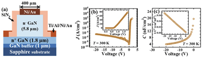
    Fig. 1. (Colour online) (a) A cross-section diagram of a GaN quasi-vertical SBD under experimentation. (b) Forward and reverse JV characteristics at 300 K presented by logarithmic scale. Inset: forward J–V characteristics at 300 K in linear scale. (c) CV characteristics at 300 K. Inset: 1/C2V curve at 300 K.
    (Colour online) (a) Energy band diagrams of hole trap in GaN for (1) capture and (2) emission process. (b) Inverted temperature-scanning ODLTS spectra. (c) Arrhenius plot for hole trap H1. (d) Apparent trap concentration profile versus depletion region width.
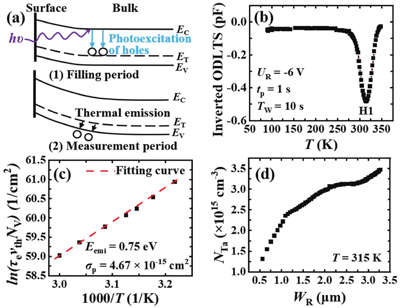
    Fig. 2. (Colour online) (a) Energy band diagrams of hole trap in GaN for (1) capture and (2) emission process. (b) Inverted temperature-scanning ODLTS spectra. (c) Arrhenius plot for hole trap H1. (d) Apparent trap concentration profile versus depletion region width.
    (Colour online) (a) Isothermal ODLTS spectra for scanning TW with fixed UR of −6 V and tp of 1 s from 315 to 343 K. (b) τe derived by isothermal ODLTS at different temperatures. (c) Arrhenius plot of trap H1 extracted from temperature-dependent τe.
    Fig. 3. (Colour online) (a) Isothermal ODLTS spectra for scanning TW with fixed UR of −6 V and tp of 1 s from 315 to 343 K. (b) τe derived by isothermal ODLTS at different temperatures. (c) Arrhenius plot of trap H1 extracted from temperature-dependent τe.
    (Colour online) (a) Electric-field-dependent τe of trap H1 extracted from capacitance transient spectra from 315 to 329 K. The ln(ep) of trap H1 as a function of (b) E2 and (c) E1/2 from 315 to 329 K. Black dotted lines are linear fitting curves.
    Fig. 4. (Colour online) (a) Electric-field-dependent τe of trap H1 extracted from capacitance transient spectra from 315 to 329 K. The ln(ep) of trap H1 as a function of (b) E2 and (c) E1/2 from 315 to 329 K. Black dotted lines are linear fitting curves.
    (Colour online) (a) Normalized capacitance transient amplitude as a function of tp. (b) Capacitance transient amplitude increases exponentially with tp. (c) τc from 315 to 343 K.
    Fig. 5. (Colour online) (a) Normalized capacitance transient amplitude as a function of tp. (b) Capacitance transient amplitude increases exponentially with tp. (c) τc from 315 to 343 K.
    Eemi (eV)0.75[44]0.70[23]0.76[20]0.75 [This work]
    NA means not applicable in the table. *This trap is related to complexes of native defects with donor impurities.
    σp (cm2)9.5 × 10⁻¹⁷NA4.9 × 10−134.67 × 10⁻¹⁵
    NTa (cm−3)1.73 × 10149.6 × 1015NA2.67 × 1015
    epENANANAPFE
    GrowthMOCVDHVPEMOCVDMOCVD
    MeasurementMCTS, 280 nmODLTS, 365 nmDLTSODLTS, 405 nm
    RemarkVGa relatedComplexes*Point defectPoint defect
    Table 1. Comparison with other published comparable hole trap in n-GaN.
    Jin Sui, Jiaxiang Chen, Haolan Qu, Yu Zhang, Xing Lu, Xinbo Zou. Emission and capture characteristics of deep hole trap in n-GaN by optical deep level transient spectroscopy[J]. Journal of Semiconductors, 2024, 45(3): 032503
    Download Citation