Jin Sui, Jiaxiang Chen, Haolan Qu, Yu Zhang, Xing Lu, Xinbo Zou. Emission and capture characteristics of deep hole trap in n-GaN by optical deep level transient spectroscopy[J]. Journal of Semiconductors, 2024, 45(3): 032503
Copy Citation Text
Emission and capture characteristics of a deep hole trap (H1) in n-GaN Schottky barrier diodes (SBDs) have been investigated by optical deep level transient spectroscopy (ODLTS). Activation energy (Eemi) and capture cross-section (σp) of H1 are determined to be 0.75 eV and 4.67 × 10?15 cm2, respectively. Distribution of apparent trap concentration in space charge region is demonstrated. Temperature-enhanced emission process is revealed by decrease of emission time constant. Electric-field-boosted trap emission kinetics are analyzed by the Poole?Frenkel emission (PFE) model. In addition, H1 shows point defect capture properties and temperature-enhanced capture kinetics. Taking both hole capture and emission processes into account during laser beam incidence, H1 features a trap concentration of 2.67 × 1015 cm?3. The method and obtained results may facilitate understanding of minority carrier trap properties in wide bandgap semiconductor material and can be applied for device reliability assessment.
Gallium nitride (GaN) has been considered as a promising material for power electronics[1] and optoelectronic devices, e.g., light emitting diodes (LEDs)[2], photodetectors[3], and solar cells[4], due to its wide energy bandgap, high electron mobility, and high thermal conductivity. However, traps in semiconductor materials may significantly impact the conductive properties and operational performance of semiconductor devices and related electronics[5−8]. Therefore, understanding the nature of traps in GaN devices holds both scientific and practical significance for improving GaN material quality and associated device efficiency.
There have been some investigations on the properties of traps in GaN-based devices. Angelotti et al. have previously extracted a shallow-level trap in a GaN radio frequency (RF) HEMT by drain current transient (DCT) analysis[9]. Using deep level transient spectroscopy (DLTS), Hierro et al. determined the carrier capture kinetics of electron traps in n-GaN[10]. DLTS holds the features of high sensitivity, high resolution, non-destructive analysis, and so on. DLTS has been performed on a variety of GaN-based devices such as Schottky barrier diodes (SBDs)[11], p−n and p−i−n junctions[12]. These studies have revealed various traps in GaN films, which are grown by various methodologies involving metal-organic chemical vapor deposition (MOCVD)[13, 14], hydride vapor phase epitaxy (HVPE)[15], and molecular beam epitaxy (MBE)[16]. Our previous work has demonstrated several majority carrier (electron) traps in n-GaN SBDs by DLTS technique using electrical pulses[17]. However, during the electrical filling pulse, a large number of majority carriers are injected in the n−-GaN layer. Thus, the DLTS signal is dominated by majority carrier traps, making the signature of minority carrier traps in the n−-GaN layer remain undetected. Minority carrier traps have significant technical implications due to their impact on carrier lifetime in some bipolar devices[18]. However, study on minority carrier traps in GaN materials is relatively challenging and limited.
The minority carrier traps could be investigated using optical deep level transient spectroscopy (ODLTS)[19, 20] or minority carrier transient spectroscopy (MCTS)[21, 22] to boost the minority carrier concentration. Polyakov et al. identified hole traps with activation energies of 0.7 and 0.9 eV in n-GaN SBDs grown on sapphire substrates using ODLTS[23, 24]. Amor et al. also revealed a hole trap characterized by activation energy of 0.76 eV utilizing DLTS, but only capture cross-section and emission time were extracted[20]. There are still some issues that need to be addressed to thoroughly understand the minority carrier trap properties in GaN materials. (i) There is still insufficient research on the detailed emission mechanism for deep hole traps, which have a significant contribution in device properties such as conductivity compensation and non-equilibrium carrier recombination[25, 26]. There is scarce information on electric-field (E) dependent emission kinetics for minority carrier traps in GaN-based materials. The electric-field in the depletion region should be taken into account since it can substantially affect the emission rate[27]. (ii) There remains a lack of quantitative analysis of the capture kinetics of deep hole traps. A comprehensive investigation into the capture kinetics of traps can reveal profound insights into the physical characteristics of defects in GaN materials[28].
In this article, we have studied emission and capture kinetics of minority carrier (hole) trap H1 in n-GaN SBD on sapphire substrate using ODLTS. Temperature-scanning ODLTS results reveal a hole trap H1 identified with activation energy of 0.75 eV and capture cross-section of 4.67 × 10⁻¹⁵ cm2. The profile of the apparent trap concentration of H1 in the space charge region has been investigated. Isothermal ODLTS for scanning measurement time (TW) and capacitance transient studies at different temperatures suggest temperature-enhanced carrier emission process and electric-field-enhanced carrier emission kinetics. The capacitance transient amplitude trends corresponding to various optical pulse width (tp) reveal the point defect type of H1 and the temperature-dependent capture kinetics. These results will provide valuable insights into the properties of minority carrier traps in GaN and contribute to the development of GaN-based devices with enhanced performance and reliability.
Experimental details
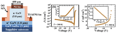
Fig. 1 (a) depicts a cross-section diagram of GaN SBD in this study. The GaN SBD was prepared by MOCVD on a 2-inch sapphire substrate. The epi-layer structure started with GaN buffer layer with 1-μm thickness and continued with n+-GaN layer with thickness of 1.8 μm and electron concentration of 5 × 1018 cm−3. Subsequently, an unintentionally-doped n−-GaN layer was deposited with thickness of 5.8 μm and carrier concentration of 5.3 × 1015 cm−3. Following etching and sidewall passivation using SiNX, a deposition of Ti/Al/Ni/Au was performed on the exposed n+-GaN layer as the cathode. Ti/Al/Ni/Au Ohmic contact underwent annealing at 850 ℃ for 30 s. On the mesa, a layer of Ni/Au with a diameter of 400 μm was deposited as the anode, and the Ni/Au Schottky contact remained unannealed. The ODLTS measurement was conducted utilizing the FT 1230 high energy resolution analysis deep level transient spectroscopy (FT 1230 HERA-DLTS) system (PhysTech) equipped with a 10 mW laser with 405 nm wavelength.
Figure 1.(Colour online) (a) A cross-section diagram of a GaN quasi-vertical SBD under experimentation. (b) Forward and reverse J–V characteristics at 300 K presented by logarithmic scale. Inset: forward J–V characteristics at 300 K in linear scale. (c) C–V characteristics at 300 K. Inset: 1/C2–V curve at 300 K.
Fig. 1(b) presents the forward and reverse current density–voltage (J–V) characteristics of the GaN SBD at 300 K. The inset of Fig. 1(b) represents forward J–V characteristics in linear scale. The threshold voltage (Vth) was identified as 0.65 V at 300 K with a current density of 1 A/cm2. Meanwhile, Fig. 1(c) depicts the capacitance–voltage (C–V) characteristics of the GaN SBD at 300 K. The frequency and AC amplitude of the C–V test were 1 MHz and 50 mV, respectively. As indicated in the inset of Fig. 1(c), 1/C2–V characteristics are plotted and present a linear relationship, suggesting that the carrier concentration is uniformly distributed. The carrier concentration (NS) was calculated as 4.59 × 1015 cm−3 from the slope of 1/C2–V (Eq. (1)).
Eemi (eV)
0.75[44]
0.70[23]
0.76[20]
0.75 [This work]
NA means not applicable in the table. *This trap is related to complexes of native defects with donor impurities.
σp (cm2)
9.5 × 10⁻¹⁷
NA
4.9 × 10⁻¹³
4.67 × 10⁻¹⁵
NTa (cm−3)
1.73 × 10¹⁴
9.6 × 10¹⁵
NA
2.67 × 10¹⁵
ep–E
NA
NA
NA
PFE
Growth
MOCVD
HVPE
MOCVD
MOCVD
Measurement
MCTS, 280 nm
ODLTS, 365 nm
DLTS
ODLTS, 405 nm
Remark
VGa related
Complexes*
Point defect
Point defect
Table 1. Comparison with other published comparable hole trap in n-GaN.
where q is the elementary charge, εr is the relative permittivity of GaN, ε0 is vacuum permittivity, and A is the anode area[11].
Temperature-scanning ODLTS spectra was employed to extract trap properties in n−-GaN layer[29, 30]. Fig. 2(a) shows energy band diagrams of capture and emission process for hole trap during the ODLTS measurement. Featuring a sub-bandgap wavelength of 405 nm, the optical pulse provides enough energy to activate the holes. A substantial number of holes are photon-excited and captured by hole trap in the n−-GaN layer during optical filling pulse period. At the end of filling period, the occupied hole trap starts to thermally emit holes for measurement period[31]. ODLTS measurement was conducted with a reverse bias (UR) of −6 V, a tp of 1 s, and a TW of 10 s. In Fig. 2(b), the inverted ODLTS spectra displays a prominent signal valley at approximately 315 K, representing a minority carrier trap. Upon application of UR of −6 V, the space charge region is located in the n−-GaN layer, accordingly, it is confirmed to be a hole trap (H1). Fig. 2(c) exhibits Arrhenius plot of the hole trap H1 resulting from the temperature-scanning ODLTS spectra. The activation energy (Eemi) and capture cross-section (σp) of the hole trap H1 were determined to be 0.75 eV and 4.67 × 10⁻¹⁵ cm2, respectively, through the Arrhenius relation[30, 32]. The σp by default represents the optical capture cross-section extracted by ODLTS[33].
Figure 2.(Colour online) (a) Energy band diagrams of hole trap in GaN for (1) capture and (2) emission process. (b) Inverted temperature-scanning ODLTS spectra. (c) Arrhenius plot for hole trap H1. (d) Apparent trap concentration profile versus depletion region width.
Fig. 2(d) illustrates apparent trap concentration (NTa) profile versus depletion region width (WR) at 315 K, obtained from the isothermal ODLTS results for scaning UR. WR was determined from C–V characteristics at 315 K by the relation[34]:
Meanwhile, apparent trap concentration (NTa) at different UR (that is, different WR) is given by[22]
where ΔC is the capacitance transient amplitude, CR is the steady-state capacitance at UR, and NS is the net carrier concentration calculated from the C–V characteristics at 315 K by Eq. (1). ΔC and CR at different UR were obtained from isothermal ODLTS measurement for scanning UR. For isothermal ODLTS measurement, tp was set to 1 s to ensure that all traps were filled. The increase of NTa with extending WR is associated with the quick carrier recombination effect at the depletion region boundary[22].
Fig. 3(a) presents the isothermal ODLTS spectra of trap H1[35, 36], which was performed from 315 to 343 K with UR of −6 V and tp of 1 s. The emission time constants (τe) were determined by extracting valley position from isothermal ODLTS spectra. As the temperature increases, the signal valley associated with trap H1 shifts towards a lower TW, indicating a decrease of τe. The τe of trap H1 at various temperatures are displayed in Fig. 3(b). It's noteworthy that the τe of H1 consistently decreased from 8.95 s at 315K to 0.74 s at 343 K, suggesting an increase of the emission rate at higher temperatures.
Figure 3.(Colour online) (a) Isothermal ODLTS spectra for scanning TW with fixed UR of −6 V and tp of 1 s from 315 to 343 K. (b) τe derived by isothermal ODLTS at different temperatures. (c) Arrhenius plot of trap H1 extracted from temperature-dependent τe.
As indicated in Fig. 3(c), the relationship between τe and temperature can be fitted by Eq. (4)[37]:
where is a constant relating to effective hole mass. From the slope and intercept of the Arrhenius plot in Fig. 3(c), the activation energy of trap H1 is determined to be 0.75 eV with a capture cross-section in the order of 10−15 cm2 as well, which is consistent with the results obtained by Fig. 2(c).
Fig. 4(a) illustrates correspondence between emission time constant (τe) and electric-field extracted from capacitance transient spectra with different UR at three different temperatures: 315, 322, and 329 K. τe decreased significantly with an increased electric-field at each temperature, which can be attributed to a reduction in the apparent thermal activation energy with the electric-field. It is also observed that τe decreased markedly with elevated temperature, which shows agreement with the conclusion in Fig. 3(b).
Figure 4.(Colour online) (a) Electric-field-dependent τe of trap H1 extracted from capacitance transient spectra from 315 to 329 K. The ln(ep) of trap H1 as a function of (b) E2 and (c) E1/2 from 315 to 329 K. Black dotted lines are linear fitting curves.
The relationship between the logarithm of the emission rate (ep) and the square of the electric-field (E2) was illustrated in Fig. 4(b). It was observed that a linear fit was not feasible, suggesting that the enhancement cannot be solely attributed to a phonon-assisted tunneling process. However, ln(ep) is plotted as a function of the square root of the electric-field (E1/2), as shown in Fig. 4(c). The linear fitting of the relationship shows that the enhancement process can be adequately described by Poole−Frenkel emission (PFE) process, which can characterize the progression of ep with E for H1 at these temperatures[38].
Fig. 5(a) displays normalized capacitance transient amplitude of trap H1 as a function of tp at various temperatures. As tp increases, capacitance transient amplitude (ΔC) first increases rapidly, which is related to the increment of the population of filled traps. As tp reaches a sufficiently long duration, all traps are completely filled, leading to saturation of ΔC.
Figure 5.(Colour online) (a) Normalized capacitance transient amplitude as a function of tp. (b) Capacitance transient amplitude increases exponentially with tp. (c) τc from 315 to 343 K.
As illustrated in Fig. 5(b), the relationship between ΔC and tp could be expressed as[39]
where ΔCmax is the saturated capacitance transient amplitude and τc is apparent capture time constant. It is observed that the curves of versus tp exhibit good linearity at several temperatures. Therefore, H1 is regarded as a point defect rather than an extended defect in terms of the excellent linear trend of curves in Fig. 5(b)[40]. From slope of linear fitting curve in Fig. 5(b), τc as a function of temperature was extracted, as shown in Fig. 5(c). From 315 to 343 K, τc was reduced from 0.18 to 0.12 s, which demonstrates a thermally enhanced capture property. Compared with capture time constants reported for majority carrier trapping process in the literatures[9, 10], the τc of minority carrier trap shows a much larger value. This is related to the small minority carrier concentration in the n-GaN material, which lower the probability of the holes getting captured, leading to a large τc for hole trap (H1)[41]. In addition, small σp (4.67 × 10⁻¹⁵ cm2) of H1 also suggested weaker capability of the hole trap to capture holes, and thus a relatively large capture time constant. The value of τc for H1 in this work is actually comparable to time constant (0.36 s) extracted for a hole trap (EV + 0.86 eV) in n-GaN using isothermal MCTS[42]. It is worth noting that τc is not equal to the time required for traps to be completely filled. The τc signifies the time it takes for the unfilled trap concentration to decrease to 1/e times NTa, shorter than the time taken for traps to be completely occupied[32].
The isothermal ODLTS spectra, depicted as a function of TW in Fig. 3(a) and tp in Fig. 5(b), can be utilized to estimate the trap concentration. For instance, at T = 315 K, the τc for the exponential relationship between the ΔC and tp is estimated to be 0.18 s. The trapped hole concentration (pt) can be computed considering the simultaneous events of hole capture and emission during laser beam incidence, according to
where cp is the hole capture coefficient, ep is the hole emission rate, p is the hole concentration, and NT is the trap concentration[43]. Under the assumption of a uniform hole concentration within the depletion region during laser beam incidence, the value of cpp can be computed as 5.44 s−1. This calculation utilizes the determined value of ep as 1/8.95 s−1, obtained from Fig. 3(a), and (cpp + ep) as 1/0.18 s−1, derived from Fig. 4(b). By employing the saturated capacitance transient amplitude ΔCmax and the corresponding relation[42]
NT is obtained to be 2.67 × 1015 cm−3. With the incident laser beam on, holes and electrons undergo optical emission, resulting in a reduction of pt. Consequently, the obtained value of NT may be underestimated. The result obtained from Eq. (7) are slightly larger than that obtained in Eq. (3), indicating the existence of a large trap concentration for hole trap H1. Trap concentration of H1 is one to two orders of magnitude larger than the concentration of majority carrier (electron) traps in our previous work[17].
Table 1 summarizes the trap characteristics of hole trap H1 in this work and other traps in literatures. The smaller σp indicates that the hole trap in the device is relatively incapable of trapping holes. Polyakov et al. have reported that the trap concentration can be reduced by three orders of magnitude by changing the device fabrication process conditions[23]. Corresponding to the different characteristics of the devices, H1 can be detected in n-GaN using different measurement techniques, i.e., MCTS[44], ODLTS[23], DLTS[20], and test conditions. H1 can be observed for materials grown by HVPE and MOCVD methods, suggesting that it is an extensive-existed defect[20, 23]. In this work, for the first time, the emission mechanism of H1 was determined to comply with the Poole−Frenkel emission model.
Conclusion
In conclusion, trap characteristics of a minority carrier (hole) trap in n-GaN SBD grown by MOCVD have been thoroughly analyzed using ODLTS. The hole trap (H1) characterized by Eemi of 0.75 eV and σp of 4.67 × 10⁻¹⁵ cm2 is considered to be a point defect. Temperature-enhanced emission and capture kinetics are investigated as the temperature increases from 315 to 343 K. This is evidenced by a significant reduction of emission time constant from 8.95 to 0.74 s and a gradual decrease of apparent capture time constant from 0.18 to 0.12 s. The emission process of H1 is found to be accelerated by electric-field, which can be well described by Poole−Frenkel emission model. In addition, the hole trap exhibits a high trap concentration of 2.67 × 1015 cm−3, taking into account that hole trapping and emission processes occur simultaneously during luminescence. These results regarding the specific properties of the deep-level trap in GaN may contribute to the advancement of GaN devices towards improved performance and reliability in power and RF electronics.
Jin Sui, Jiaxiang Chen, Haolan Qu, Yu Zhang, Xing Lu, Xinbo Zou. Emission and capture characteristics of deep hole trap in n-GaN by optical deep level transient spectroscopy[J]. Journal of Semiconductors, 2024, 45(3): 032503