
Qiurong Deng, Jianfeng Chen, Li Long, Baoqin Chen, Huakang Yu, Zhiyuan Li. Silicon cuboid nanoantenna with simultaneous large Purcell factor for electric dipole, magnetic dipole and electric quadrupole emission[J]. Opto-Electronic Advances, 2022, 5(2): 210024
- Opto-Electronic Advances
- Vol. 5, Issue 2, 210024 (2022)
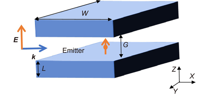
Fig. 1. Schematic of the silicon cuboid dielectric optical nanoantenna.
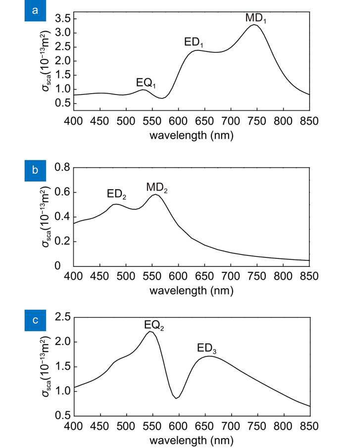
Fig. 2. Calculated scattering cross section for a silicon cuboid nanoantenna with the width W of 220 nm, the length L of 40 nm, and the gap size G of 20 nm upon the plane wave illumination under different plane wave incidence directions and polarizations as follows: (a ) Negative y-axis incidence direction and Ex polarization, (b ) negative y-axis incidence direction and Ez polarization, and (c ) positive z-axis incidence direction and Ey polarization.
Fig. 3. Polarization charge (ρ) distribution [panels (a ), (c ) and (e )] and electric field (E ) amplitude distribution [panels (b ), (d ) and (f ), color plots] calculated on the specified cutting plane of the nanoantenna at the resonance wavelength of the ED1, ED2 and ED3 mode shown in Fig. 2 respectively. Panel (b) is for the central XZ plane, panel (d) is for the central XZ plane, while panel (f) is for the central YZ plane of the cuboid nanoantenna. The black arrows show the direction of electric field and the length of the arrow denotes the field intensity.
Fig. 4. Polarization charge ( a ) and (b )] and electric field (E ) amplitude distribution [panels (c ) and (d ), color plots] calculated on the specific cutting plane of the nanoantenna at the resonance wavelength of EQ1 and EQ2 mode shown in Fig. 2, respectively. Panel (c) is for the central XY plane (i.e., the mid-gap plane), while panel (d) is for the central YZ plane of the cuboid nanoantenna. The black arrows show the direction of electric field and the length of the arrow denotes the field intensity.
Fig. 5. Polarization charge ( a ) and (b )] and magnetic field (H) amplitude distribution [panels (c ), (d ), and (e ), (f ), color plots] calculated on the specific cutting plane of the nanoantenna at the resonance wavelength of MD1 and MD2 mode shown in Fig. 2, respectively. Magnetic field calculated on the cutting plane at the MD resonances [panels (c)–(f)]. Panel (c) is for the central XY plane (i.e., the mid-gap plane), panel (d) is for the central YZ plane, while panel (e) and (f) are for the central XZ plane of the cuboid nanoantenna. The black arrows superimposed in panels (c) and (d) show the direction and strength of magnetic field, while in panels (b) and (c) they illustrate the electric polarization (P ) distribution (and thus the polarized electric current j distribution).
Fig. 6. The radiative decay rate enhancement factors as a function of wavelength for (a ) ED, MD [(b ) and (d )], and EQ [(c ) and (e )] emitter located at the center of the silicon cuboid nanoantenna. The ED emitter has an orientation parallel to the z-axis, the MD emitter has an orientation parallel to the z-axis (b) and x-axis (c ), while the EQ emitter has an orientation within the YZ plane(d) and XY plane(e ). The width of the cuboid is 220 nm, the length is 40 nm, and the gap size is 20 nm.
Fig. 7. The polarization charge distribution for (a ) an ED point emitter oscillating at 475 nm, (b ) a MD point emitter oscillating at 750 nm, and (c ) an EQ point emitter oscillating at 556 nm. All the emitters are located at the center of the silicon cuboid nanoantenna.


Set citation alerts for the article
Please enter your email address

© Copyright 2018-2021 | Chinese Laser Press. All Rights Reserved 沪ICP备15018463号-20