Qiurong Deng, Jianfeng Chen, Li Long, Baoqin Chen, Huakang Yu, Zhiyuan Li. Silicon cuboid nanoantenna with simultaneous large Purcell factor for electric dipole, magnetic dipole and electric quadrupole emission[J]. Opto-Electronic Advances, 2022, 5(2): 210024
Copy Citation Text
The Purcell effect is commonly used to increase the spontaneous emission rate by modifying the local environment of a light emitter. Here, we propose a silicon dielectric cuboid nanoantenna for simultaneously enhancing electric dipole (ED), magnetic dipole (MD) and electric quadrupole (EQ) emission. We study the scattering cross section, polarization charge distribution, and electromagnetic field distribution for electromagnetic plane wave illuminating the silicon dielectric cuboid nanoantenna, from which we have identified simultaneous existence of ED, MD and EQ resonance modes in this nanoantenna. We have calculated the Purcell factor of ED, MD and EQ emitters with different moment orientations as a function of radiation wavelength by placing these point radiation source within the nanoantenna, respectively. We find that the resonances wavelengths of the Purcell factor spectrum are matching with the resonance modes in the nanoantenna. Moreover, the maximum Purcell factor of these ED, MD and EQ emitters is 18, 150 and 118 respectively, occurring at the resonance wavelength of 475, 750, and 562 nm, respectively, all within the visible range. The polarization charge distribution features allow us to clarify the excitation and radiation of these resonance modes as the physical origin of large Purcell factor simultaneously occurring in this silicon cuboid nanoantenna. Our theoretical results might help to deeply explore and design the dielectric nanoantenna as an ideal candidate to enhance ED, MD and EQ emission simultaneously with very small loss in the visible range, which is superior than the more popular scheme of plasmonic nanoantenna.
Introduction
Spontaneous emission (SE) of quantum emitters, such as molecules, rare earth ions, and quantum dots into free space, is a key phenomenon across the whole area of quantum optics. The control of spontaneous emission is a critical step in designing various optical elements and devices, such as nanoantenna, hyperbolic metamaterial, light-emitting diode, single-photon sources, nano-lasers, and signals detection1-8. As first demonstrated by E.M. Purcell in 1946 in the context of nuclear magnetic resonance, the Purcell effect describes that the spontaneous emission of a quantum emitter is not an intrinsic property of the emitter, but can be modified by its interaction with environment9. The Purcell factor is used to evaluate the enhancement extent of the SE rate by the emitters. Strong Purcell effect is usually accomplished by placing emitters in microcavities, nanoantennas, photonic crystals or meta-materials6-15. This effect now is widely used in efficient laser operation1, single-photon sources16-18, fluorescent microscopy and nanoscale imaging19-21, biological studies22, and spectroscopy23.
One important property of nanoantennas is their ability to concentrate electromagnetic energy at the nanoscale. Plasmonic nanoantennas exhibits extraordinary surface plasmon resonances that create a highly localized electric field and increase photon local density of states, resulting in the enhancement of SE rate. However, the effect is accompanied by unwanted large losses due to strong metal absorption. In contrast, dielectric nanoantennas with high permittivity and supporting strong Mie resonances provide a potential to realize low loss manipulation of light scattering24-26. Recent works showed that dielectric nanosphere can have both electric dipole (ED) and magnetic dipole (MD) resonance modes simultaneously excited inside the same particle upon the plane wave illumination26-28. It provides a canonical example of dielectric antennas that can be used to enhance MD emission. Researchers have also calculated the contributions of different multipoles, including ED, MD and electric quadrupole (EQ) mode to the optical scattering cross sections for Si nanoparticles with different sizes in the visible to infrared range26, 29, 30.
ED emission can be enhanced through plasmonic and dielectric nanoantenna31-33, while MD emission can be enhanced through split ring resonance34, diabolo antenna35, dielectric antenna36-38, and sandwiched structure39, 40. Several researchers have shown to enhance both ED and MD emission by silicon nanosphere or plasmonic antenna41, 42, and others have also shown to enhance ED, MD and EQ emission by the plasmonic sandwiched structure43. However, the enhancement factor among the emitters has different magnitudes that are not always satisfactorily large. Moreover, plasmonic nanostructures suffer from high dissipation loss compared with dielectric nanostructures. On the other hand, it has been well established that dielectric nanospheres of sufficiently large size can exhibit the ED, MD and EQ resonance modes upon the plane wave illuminated, and they have been used to enhance the MD emission26 ,or to enhance the ED and MD emission with different nanospheres sizes respectively,30 or to realize the excitation enhancement in two-photon-induced and three-photon-induced absorption44. However, it remains unclear whether these dielectric nanospheres or other more general dielectric nanostructures can be utilized to simultaneously enhance the spontaneous emission from ED, MD and EQ with very low loss and with large magnitude.
In this paper, we handle this issue and systematically investigate controlling spontaneous emission of ED, MD and EQ emitters by a designed silicon dielectric cuboid nanoantenna. We first study the resonance modes in this dielectric nanostructure upon three different orientations of incident plane wave. Then we carefully calculate and analyze the Purcell factor of ED, MD and EQ emitter with different orientations located at the center of the cuboid nanoantenna. We find that the silicon cuboid nanoantennas can simultaneously enhance ED, MD and EQ emission by a large magnitude. Finally, we discuss the relationship between the resonance modes in the dielectric cuboid nanoantenna and the Purcell factor of an ED, MD or EQ emitter located at the center of the nanoantenna.
Structure and method
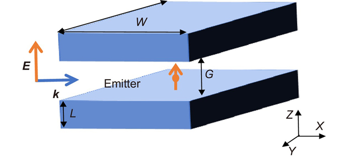
The structure we consider is shown schematically in Fig. 1. The nanoantenna is made of two silicon patches, separated with a gap side G of 20 nm. The width W and length L of the silicon cuboid is 220 nm and 40 nm respectively. A plane wave incident light is used to investigate the scattering properties of the structure. After that, an emitter is placed at the center of the nanogap antenna. With the assistance of the nanoantenna, the radiation power of the emitter can be significantly enhanced compared with the situation when the emitter is placed in free space.
Figure 1.Schematic of the silicon cuboid dielectric optical nanoantenna.
The whole structure is simulated by finite element method. In all the calculations, the cuboid nanoantenna is placed in vacuum. The refractive index of silicon is fitted from experimental data from ref.45 and then the permittivity of silicon is calculated from the refractive index . In order to investigate the scattering properties of the structure, we have first calculated the scattering cross sections when the structure is impinged by different polarized plane waves. The scattering cross section is calculated as
where is the total scattered power and is the intensity of incident plane wave. To explore the modification of the SE rate for ED, MD and EQ emitters located in the gap of cuboid nanoantenna, we use the Purcell factor, which is defined as the ratio of the SE rate with structure ( ) and the SE rate without structure ( )46. The enhancement of the SE rate can be equivalently calculated from the power normalized to the case in vacuum47. The total decay rate of the emitter includes both the radiative part and the nonradiative part due to absorption. To this end, the total power P can be separated into the radiating power and the absorption power (due to material loss of silicon) . Therefore, the Purcell factor of the radiation decay rate enhancement part in this paper is,
where stands for the power radiated to the far field by the reference emitter in vacuum. By using finite element analysis, we can now evaluate the radiation power to obtain the Purcell factors of ED, MD and EQ emission.
Analysis of resonance modes in nanoantenna
We first explore the scattering properties of the silicon nanoantenna upon electromagnetic excitation by plane wave illumination. This will reveal its electromagnetic resonances and provide information on its interactions with ED, MD, and EQ emitter. We consider three different polarized plane waves, calculate and show the corresponding scattering cross sections in Fig. 2(a–c), respectively. In the calculated scattering spectrum, a strong MD resonance (MD1 mode) at 743 nm, an ED resonance (ED1 mode) at 637 nm, and an EQ resonance (EQ1 mode) at 531 nm are observed with the plane wave propagating along the negative y direction and with the polarization, as seen in Fig. 2(a). We also find an ED resonance (ED2 mode) at 481 nm and an MD resonance (MD2 mode) at 556 nm upon the plane wave illuminated along the negative y direction and with the polarization, as found in Fig. 2(b). When the structure is impinged by a plane wave along the z direction and with the polarization, an ED resonance (ED3 mode) and an EQ resonance (EQ2 mode) are found at 656 nm and 541 nm, respectively, as seen in Fig. 2(c). These resonances modes are typically expected for a high-index dielectric nanoparticle26, 27.
Figure 2.Calculated scattering cross section for a silicon cuboid nanoantenna with the width W of 220 nm, the length L of 40 nm, and the gap size G of 20 nm upon the plane wave illumination under different plane wave incidence directions and polarizations as follows: (a) Negative y-axis incidence direction and Ex polarization, (b) negative y-axis incidence direction and Ez polarization, and (c) positive z-axis incidence direction and Ey polarization.
In order to have deeper insight into the resonance modes and confirm the validity of the above classification against them, the polarization charge distributions and the electromagnetic field distribution at these resonance modes on the top or side view of the silicon nanoantenna are calculated and shown in Figs. 3–5. We have assumed that the incident electric field E has an amplitude of 1 V/m. All the electromagnetic fields E and H are normalized to those of the incident fields, and the polarization charge densities are all in unit of .
The red and blue color represents positive and negative polarization charges, respectively. We can see from Fig. 3(a) that the positive and negative polarization charges at the ED1 resonance intensively, and mainly distribute on the two YZ end surfaces of silicon patches; from Fig. 3(e) we see that they are intensively concentrated at the two XZ end surfaces of silicon patches at the ED3 resonance; while from Fig. 3(c) we see that they mainly distribute on the two inner XY surfaces of silicon patches at the ED2 resonance. These distribution features are consistent with the polarization state of the incident plane wave, which is along the x-axis, y-axis, and z-axis for the ED1, ED3, and ED2 modes, respectively. To further illustrate these three ED resonance modes, we plot in Fig. 3(b), 3(d) and 3(f) the electric field distribution at the resonance wavelength and in the corresponding cutting cuboid plane. The electric field intensity of the ED1, ED2, and ED3 modes exhibits a dipole distribution at XZ, XZ and YZ cutting plane respectively. Furthermore, the electric field direction of these three ED modes is in the negative x direction, negative z direction, and y direction, respectively. These features are consistent with the positive and negative polarization charges distribution profiles and the polarization direction plotted in Fig. 3(a), 3(c) and 3(e), which is along the x-axis, z-axis, and y-axis for the ED1, ED2, and ED3 modes. The electric field intensity and direction both have a dipole distribution profile, which is similar to the distribution of ED emitter, and this once again confirms a resonating ED mode under the excitation of incident electromagnetic waves.
We can see from Fig. 4(a) that the positive and negative polarization charges at the EQ1 resonance are concentrated alternately on the four corners of the XY plane of the silicon patches, while polarization charges of same sign distribute on the same diagonal of XY plane. This feature is similar to two electric dipoles in opposite directions distributing in the XY cutting plane. From Fig. 4(b) we see that the positive and negative polarization charges are concentrated alternately on the four inner corners of the YZ plane of the silicon patches at the EQ2 resonance, while charges of same sign distribute on the same diagonal of YZ plane. This is similar to two opposite directed electric dipoles distributing in the YZ cutting plane. The corresponding electric field distributions at EQ1 and EQ2 resonances wavelengths are shown in Fig. 4(c) and 4(d). The electric field intensity of the EQ1 and EQ2 modes has a quadrupole distribution at the XY and YZ cutting plane, respectively. The electric field intensity distributions are consistent with the polarization charge distribution, which are alternately distributed in the XY and YZ cutting planes, respectively. The electric field direction of EQ1 resonance mode is oriented along the diagonal of the XY cutting plane, following the charges polarization direction plotted in Fig. 4(a).
Figure 3.Polarization charge (ρ) distribution [panels (a), (c) and (e)] and electric field (E) amplitude distribution [panels (b), (d) and (f), color plots] calculated on the specified cutting plane of the nanoantenna at the resonance wavelength of the ED1, ED2 and ED3 mode shown in Fig. 2 respectively. Panel (b) is for the central XZ plane, panel (d) is for the central XZ plane, while panel (f) is for the central YZ plane of the cuboid nanoantenna. The black arrows show the direction of electric field and the length of the arrow denotes the field intensity.
Furthermore, the electric field direction of EQ2 resonance mode also follows the charges polarization direction plotted in Fig. 4(b), orienting along the four sides of YZ cutting plane of silicon patches. The electric field intensity and direction in both cases have a quadrupole distribution to resemble the EQ resonance mode.
We can see from Fig. 5(a) that the positive and negative polarization charges at the MD1 resonance are somewhat uniformly distributed at the whole edges of silicon patches surrounding the z-axis, while from Fig. 5(b) we see that they are somewhat uniformly distributed at the whole edges of silicon patches surrounding the x-axis at the MD2 resonance. The corresponding distribution of magnetic field (H) with both strength and direction, and electric polarization (P) at the resonance wavelength are calculated and plotted in Fig. 5 for further illustration. The electric polarization distribution, illustrated by arrows superimposed upon the magnetic field pattern in Fig. 5(c) and 5(d), shows a current loop flowing in the XY and YZ cutting planes, respectively, which is consistent with the polarization charges distribution. Thus, the magnetic field direction is oriented along the z-axis and x-axis for the MD1 and MD2 modes. As shown in Fig. 5(e) and 5(f), the magnetic field direction is pointing to the z-axis direction and x-axis direction. Furthermore, the magnetic field intensity and direction show a magnetic dipole feature. The fact that magnetic field has a dipole distribution and polarization shows a current loop flowing clearly indicates the occurrence of MD resonance mode excited by the incident electromagnetic wave at these two particular wavelengths.
Figure 4.Polarization charge ( ) distribution [panels (a) and (b)] and electric field (E) amplitude distribution [panels (c) and (d), color plots] calculated on the specific cutting plane of the nanoantenna at the resonance wavelength of EQ1 and EQ2 mode shown in Fig. 2, respectively. Panel (c) is for the central XY plane (i.e., the mid-gap plane), while panel (d) is for the central YZ plane of the cuboid nanoantenna. The black arrows show the direction of electric field and the length of the arrow denotes the field intensity.
Comparing the magnitude of polarization charge density of the ED, MD, and EQ resonance modes as displayed in Figs. 3–5, we find that the ED resonances modes have lower density than that of the EQ and MD resonances modes, while the EQ and MD resonance modes have similar polarization charge density. All these features can help to reveal the extent of Purcell factor for an ED, MD, or EQ emitter that are situated at the center of the cuboid nanoantenna structure discussed above, which supports three types of resonance modes, simultaneously. On the other hand, our calculations have shown that although silicon has nonzero absorption coefficient, the absorption cross section is much smaller than the scattering cross section for the silicon structure, while the absorption cross section is comparable to the scattering one for the silver structure in the visible range (data not shown here). Therefore, the current silicon dielectric nanoantenna structure is superior to plasmonic structure in terms of absorption loss and dissipation. In addition, one can also use other non-absorptive materials such as TiO2 to construct nanoantenna to further reduce absorption loss and dissipation.
Figure 5.Polarization charge ( ) distribution [panels (a) and (b)] and magnetic field (H) amplitude distribution [panels (c), (d), and (e), (f), color plots] calculated on the specific cutting plane of the nanoantenna at the resonance wavelength of MD1 and MD2 mode shown in Fig. 2, respectively. Magnetic field calculated on the cutting plane at the MD resonances [panels (c)–(f)]. Panel (c) is for the central XY plane (i.e., the mid-gap plane), panel (d) is for the central YZ plane, while panel (e) and (f) are for the central XZ plane of the cuboid nanoantenna. The black arrows superimposed in panels (c) and (d) show the direction and strength of magnetic field, while in panels (b) and (c) they illustrate the electric polarization (P) distribution (and thus the polarized electric current j distribution).
Having characterized the ED, MD and EQ resonance modes upon the plane-wave excitation, we now study the Purcell factor for an ED, MD, or EQ emitter situated at the center of the same cuboid nanoantenna structure. We have set that the ED have their dipole moment orientation parallel to the z-axis, the MD emitters have their dipole moment orientation parallel to the z-axis or x-axis, while the EQ emitter has an orientation within the YZ plane or XY plane. The simulation results of the Purcell factor spectrum, i.e., Purcell factor as a function of radiation wavelength, are shown in Fig. 6. One can see clearly that the spontaneous emission rate of the three types of emitters can be enhanced simultaneously by the cuboid nanoantenna. It is observed from Fig. 6(a) that the Purcell factor reaches a peak value of 18 at 475 nm for the ED emitter when it has a dipole moment orientation parallel to the z-axis. This resonance wavelength fits with the resonance wavelength of the ED2 mode (481 nm) investigated above in Fig. 2(b). The excitation configuration of plane wave investigated in Fig. 2(b), propagating along the negative y direction and with polarization, is similar to the configuration for this orientation of point ED emitter. In contrast, an ED emitter with a dipole moment orientation parallel to the x-axis (or y-axis) is hard to get its emission by the cuboid nanoantenna.
We can see from Fig. 6(b) that the Purcell factor reaches a peak value of 150 at 750 nm for the MD emitter when it has a dipole moment orientation parallel to the z-axis, while the Purcell factor reaches a peak value of 38 at 556 nm for the MD emitter oriented parallel to the x-axis, as seen from Fig. 6(c). These two resonance wavelengths are consistent with the resonance wavelength of MD1 and MD2 modes as displayed in Fig. 2(a) and 2(b), which is 743 nm and 556 nm, respectively. From the discussion about the MD resonance modes above, the magnetic field direction is oriented along the z-axis and x-axis for the MD1 and MD2 modes, which is consistent with the magnetic dipole moment orientation investigated in Fig. 6(b) and 6(c), respectively. Through comparing the Purcell factor of these two MD emitters, we find that the emitter with the z-axis dipole moment orientation can better enhance the MD radiation when it is situated at the center of the cuboid nanoantenna.
Figure 6.The radiative decay rate enhancement factors as a function of wavelength for (a) ED, MD [(b) and (d)], and EQ [(c) and (e)] emitter located at the center of the silicon cuboid nanoantenna. The ED emitter has an orientation parallel to the z-axis, the MD emitter has an orientation parallel to the z-axis (b) and x-axis (c), while the EQ emitter has an orientation within the YZ plane(d) and XY plane(e). The width of the cuboid is 220 nm, the length is 40 nm, and the gap size is 20 nm.
It is observed from Fig. 7(d) that the EQ emitter Purcell factor spectrum reaches a maximum of 115 at wavelength 562 nm when the EQ emitter has an orientation within the YZ plane. The resonance wavelength is consistent with the EQ2 resonance position at 541 nm plotted in Fig. 2(c). From the discussion about the EQ2 mode above, the polarization charge distribution is similar to two oppositely directed electric dipoles distributing in the YZ cutting plane, which is consistent with the quadrupole moment orientation of EQ emitter. Furthermore, we can see from Fig. 6(e) that the Purcell factor reaches a peak value of 13 at 531 nm and a peak value of 67 at 756 nm when the EQ emitter has an orientation within the XY plane. The resonance wavelength (531 nm) is consistent with the resonance wavelength of EQ1 mode (531 nm) plotted in Fig. 2(a). From the discussion about the EQ2 mode above, the polarization charges distribution is similar to two opposite directed electric dipoles distributing in the XY cutting plane, which is consistent with the quadrupole moment orientation of EQ emitter. The second peak value of Purcell factor spectrum (at 756 nm) is matching well with the resonance wavelength of MD1 mode. This indicates that the Purcell factor spectrum at 756 nm is possibly affected by the MD1 mode and the EQ emitter at this wavelength has much possibility to excite the MD1 mode because of their similarity in major profile of polarization charge distribution. Through comparing the Purcell factor of these two EQ emitters, we find that the emitter with a quadrupole moment orientation within the XY plane can better improve the EQ radiation by situating it at the center of the cuboid nanoantenna.
Figure 7.The polarization charge distribution for (a) an ED point emitter oscillating at 475 nm, (b) a MD point emitter oscillating at 750 nm, and (c) an EQ point emitter oscillating at 556 nm. All the emitters are located at the center of the silicon cuboid nanoantenna.
Now we can see that the Purcell factor spectrum of an ED, EQ or MD emitter with specific orientation parallel to z-axis, within the YZ plane, and parallel to z-axis can reach a high maximum value of 18, 115 and 150, respectively for a radiation wavelength distributed at 475, 562, and 750 nm, all within the visible range. The Purcell factor of MD and EQ emitter has the same order of magnitude, while they are one order of magnitude larger than that of the ED emitter. This is consistent with the feature of polarization charge density at the ED, MD and EQ resonance modes, where we have seen that the polarization charge density at ED resonances is lower than the polarization charge density at EQ and MD resonances, while the latter two have similar density. Therefore, it can be further confirmed that the intensity and wavelength of ED, MD and EQ resonances modes existing in the cuboid nanoantenna do determine the major profile of the Purcell factor spectrum of these emitters.
In order to further illustrate the above connection deeply, the polarization charges distribution at the several typical resonance wavelengths of the Purcell factor spectrum is calculated and plotted in Fig. 7. The polarization charge densities are all in unit C/m3.When an ED emitter is situated at the center of the cuboid nanoantenna and its orientation is parallel to z-axis, as displayed in Fig. 7(a), the positive and negative charges respectively distribute on each patch of the structure along the z-axis for an oscillating wavelength of 475 nm, which is consistent with the polarization charges distribution at ED2 resonance mode displayed in Fig. 3(c). Furthermore, as shown in Fig. 7(b), the positive and negative charges are alternatingly distributed at the whole edges of silicon patches surrounding the z-axis for an MD emitter oriented parallel to z-axis for an oscillating wavelength of 750 nm, which is similar to the polarization charges at MD2 resonance mode displayed in Fig. 5(a), where they are somewhat uniformly distributed at the whole edges of silicon patches surrounding the z-axis. As plotted in Fig. 7(c), the positive and negative polarization charges at the resonance wavelength (556 nm) for an EQ emitter situating at the center of the cuboid nanoantenna and having an orientation within the YZ plane are concentrated alternately on the four inner corners of the YZ plane of the silicon patches, while charges of same sign distribute on the same diagonal of YZ plane. This distribution feature is consistent with the polarization charges distribution at EQ2 resonance mode plotted in Fig. 4(b). It is similar to two oppositely directed electric dipoles distributed in the YZ cutting plane, and this feature is well consistent with the orientation of EQ emitter. The above analyses on the polarization charge distribution profile once again confirm the excitation and radiation of the ED, MD, and EQ resonance modes as the physical origin of large Purcell factors simultaneously occurring in this silicon cuboid nanoantenna.
Conclusion
In summary, we have identified the ED, MD and EQ resonant modes existing in a silicon dielectric cuboid nanoantenna that is excited by incident plane wave with different polarized states through investigating systematically the scattering cross section, polarization charge distribution, and electromagnetic field distribution of this antenna. We have found that such a silicon cuboid nanoantenna can simultaneously enhance ED, MD and EQ emission with much less absorption loss compared with more popular scheme of plasmonic structure nanoantenna. We have calculated the Purcell factor spectrum of an ED, MD or EQ emitter with different moment orientation located at the center of the dielectric cuboid nanoantenna. The enhancement factor can reach a high maximum value of 18, 150 and 115, respectively for a radiation wavelength distributed at visible range as 475 nm, 750 nm, and 562 nm with specific moment orientation. Moreover, the resonance wavelength of the Purcell factor spectrum is consistent with that of the resonance modes with similar orientation. The fact that the resonance wavelength and intensity of the Purcell factor spectrum are determined by the resonance modes in the dielectric cuboid nanoantenna clearly indicate that the radiation power of these emitters is enhanced via the excitation of the corresponding ED, MD, or EQ resonance modes as a secondary radiation source (might be called synthetic emitter) with a much larger effective moment. This feature has been further confirmed by analyzing the polarization charge distribution excited by these emitters. We expect that our theoretical results might help to deeply explore and design the dielectric nanoantenna as an ideal candidate to control ED, MD and EQ emission simultaneously with very small loss in the visible range that might be superior than the more popular scheme of plasmonic nanoantenna.
Qiurong Deng, Jianfeng Chen, Li Long, Baoqin Chen, Huakang Yu, Zhiyuan Li. Silicon cuboid nanoantenna with simultaneous large Purcell factor for electric dipole, magnetic dipole and electric quadrupole emission[J]. Opto-Electronic Advances, 2022, 5(2): 210024