Abstract
To achieve high quality lighting and visible light communication (VLC) simultaneously, GaN based white light emitting diodes (WLEDs) oriented for lighting in VLC has attracted great interest. However, the overall bandwidth of conventional phosphor converted WLEDs is limited by the long lifetime of phosphor, the slow Stokes transfer process, the resistance-capacitance (RC) time delay, and the quantum-confined Stark effect (QCSE). Here by adopting a self-assembled InGaN quantum dots (QDs) structure, we have fabricated phosphor-free single chip WLEDs with tunable correlated color temperature (CCT, from 1600 K to 6000 K), a broadband spectrum, a moderate color rendering index (CRI) of 75, and a significantly improved modulation bandwidth (maximum of 150 MHz) at a low current density of . The broadband spectrum and high modulation bandwidth are ascribed to the capture of carriers by different localized states of InGaN QDs with alleviative QCSE as compared to the traditional InGaN/GaN quantum well (QW) structures. We believe the approach reported in this work will find its potential application in GaN WLEDs and advance the development of semiconductor lighting-communication integration.1. INTRODUCTION
Visible light communication (VLC) has attracted great attention in recent years due to its advantages of high security, high speed, and no RF interference [1,2]. The choice of VLC transmitters has an advantage of being embedded with WLEDs towards the integration of lighting and communication. GaN light-emitting diode (LED) based semiconductor lighting has spread and gradually penetrated indoor lighting application [3,4]. At present, the widely adopted approach for lighting-oriented white LEDs (WLEDs) is to utilize the blue LED to excite the yellow phosphors (YAG:Ce) [5]. However, the overall bandwidth of the above-mentioned phosphor converted WLED is only a few MHz [6], mainly limited by the following factors: the long lifetime of YAG:Ce phosphor and slow Stokes transfer process [7]; a resistance-capacitance (RC) time delay of the broad area WLEDs; the quantum-confined Stark effect (QCSE), and the InGaN/GaN quantum wells (QWs) from intrinsic piezoelectric polarization filed [8]. Besides, the YAG:Ce phosphor exhibits some disadvantages of wide emission spectrum, absence of red spectrum component, large particles size (), color conversion, and phosphors efficiency droop [9].
Some approaches are proposed to overcome the above-mentioned limits. Novel color conversion materials are developed, such as conjure polymer, quantum dots (QDs), and carbon dots [10–14]. Even though they have a typical short fluorescence lifetime in the order of several or tens of nanoseconds, the performance of WLEDs for lighting with the new color conventional materials needs to be improved. Micro-LED is usually used to reduce the RC time delay and release the polarization field. However, a chip that is too small is not suitable for lighting applications. Especially what should be noted is that the reported VLC oriented micro-LEDs are operated at substantially high current density, normally over [15], which is obviously not suitable for real application due to the severe efficiency droop of micro-LEDs and the heat dissipation issue. Epitaxial growth on a semi-polar or non-polar plane is feasible yet the growth process is complicated and needs to improve the material quality further [16,17]. Structures such as resonant cavity LEDs (RC LEDs) and photonic crystal LEDs (PhC LEDs) have been studied and the design and fabrication is also complicated [8,18,19]. Red, green, and blue tri-color LED chips together can achieve a higher modulation bandwidth, yet the modulation is complex for communication [20].
Here we demonstrate a phosphor-free broadband spectrum single chip WLED by employing a self-assembled InGaN QDs structure, which exhibits tunable correlated color temperature (CCT, from 1600 K to 6000 K), a maximum color rendering index (CRI) of 75, and a large modulation bandwidth of 150 MHz at a low current density of . Compared to traditional InGaN/GaN QWs structures, the self-assembled QDs can significantly reduce the built-in piezoelectric polarization field, leading to an alleviation of QCSE. The slow phosphor and Stokes transfer process can be eliminated in this phosphor-free structure. Furthermore, the quasi-three-dimensional confinement of carriers in the InGaN/GaN QDs inhibits non-radiative recombination due to the localization effect. Consequently, our reported InGaN QDs based single chip WLEDs show potential in meeting both lighting and fast VLC applications.
Sign up for Photonics Research TOC. Get the latest issue of Photonics Research delivered right to you!Sign up now
2. EXPERIMENTS
In our study, the epitaxial growth was on a c-plane (0001) sapphire substrate by metalorganic chemical vapor deposition (MOCVD). The schematic epitaxial structure is shown in Fig. 1(a), which consists of a 3 μm-thick undoped-GaN layer, a 3-μm-thick Si-doped n-GaN layer, multiple quantum wells (MQWs), followed by a 20 nm thick p-AlGaN electron blocking layer (EBL) and a 200 nm thick p-GaN layer. A 0.5 nm thin wetting layer was inserted before the InGaN well layer. A relatively high pressure of 600 mbar was employed for the following growth of MQWs. Under a high reactor pressure, more organic molecules will be cracked and then deposited on the surface, leading to a shorter mean free path for indium adatoms on the top of the wetting layer, which promotes the segregation of In adatoms for forming In-rich regions clusters in favor of 3D growth [21].
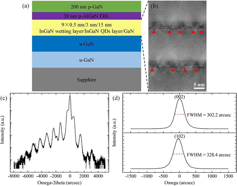
Figure 1.(a) Schematic epitaxial structure. (b) HRTEM image of the QWs. (c) scan of the epitaxial layer. (d) -scan rocking curves of (0002) and (10-12) planes.
The LED devices were fabricated using a conventional mesa structure method with a chip size of . Current-voltage (I-V) property was measured using a Keithley 2400 source meter. Electroluminescence (EL) spectra were measured by an integrating sphere. To measure the electrical bandwidths of the LEDs, an AC small signal from port 1 of a Agilent network analyser (NA) (E5061B) was added to a DC bias using a bias tee and then to drive the LED. Output light was collimated by a transmitter lens and focused by a receiver lens, which was then detected by a high-speed 1.2 GHz PIN photodetector (Newport 818-BB-21A) and sent to port 2 of the NA to analyze the frequency response of the LED.
3. RESULTS AND DISCUSSION
The high resolution transmission electron microscopy (HRTEM) image of MQWs region is shown in Fig. 1(b) where the alternately stacked layers of bright and dark represent GaN quantum barriers (QBs) and InGaN QWs, respectively. In QWs, it can be clearly observed that the dark dots with inhomogeneously and randomly distributed size and shape are considered to be InGaN QDs (as indicated by the red mark). This is due to a serious indium phase separation as well as an indium compositional fluctuation in the high indium component InGaN QW, resulting in InGaN QDs self-assembled in the InGaN matrix by the InGaN clustering effect. The average indium content is estimated to be about 39% by high-resolution X-ray diffraction (HRXRD) measurements shown in Fig. 1(c). The surface morphology of uncapped InGaN QDs can refer to Ref. [21], with density to be and diameter to be . Satellite peaks are observed, confirming the periodic characteristics of MQWs. The absence of sub-satellites peaks reveals that the QW/QB interfaces are disturbed due to In fluctuation. The full width at half maximum (FWHM) of (0002) and (10-12) planes -scan rocking curves is 302.2 arcsec and 328.4 arcsec, respectively [Fig. 1(d)].
The optical properties of the InGaN QDs were studied using temperature dependent photoluminescence (TDPL) and time-resolved photoluminescence (TRPL). Figure 2(a) shows the TDPL spectra from 10 K to 300 K. The corresponding peak emission wavelength and the FWHM of spectra are plotted in Fig. 2(b). There is a weak red shift at 50 K and a monotonical blue shift from 574.5 nm to 570.5 nm, with the temperature increasing from 50 K to 300 K. Different from the traditional InGaN/GaN QWs, the blue shift of the emission peak with the increasing temperature can be regarded as strong evidence of a carrier localization effect [22–24]. When the temperature is very low (5 K), carriers are considered immobile, so they can overcome the potential fluctuations and relax rapidly into the local minimum potential with the increase of temperature, resulting in an initial red shift of the emission peak. As temperature continues to increase, the band filling effect in the deep localization states is gradually enhanced, and the carriers are delocalized to escape from potential minima, resulting in a blue shift of the emission peak and the increase of FWHM. In our sample, the blue shift of emission peak and the increase of FWHM were relatively small, indicating that only a small part of the carriers escaped from the potential minima. The internal quantum efficiencies (IQEs) are calculated to be 30% [25,26], which is relatively high for InGaN based LEDs with high In content. The PL decay curve at 300 K is shown in Fig. 2(c), and can be fitted well by a double-exponential function [27,28]: where is the PL intensity, and are constants, and and represent the fast and slow decay time, respectively. According to the fitting result, is 3.8 ns and is 76.8 ns. The electrical bandwidths can be expressed simply as follows [29]: where is the effective carrier lifetime, and . Therefore, it can be obtained that the corresponding bandwidth is 76 MHz, which is higher than the bandwidth of broad-area blue LED ().

Figure 2.(a) TDPL spectra of the InGaN QDs sample. (b) Peak wavelength and FWHM of TDPL spectra versus measurement temperatures. (c) PL decay curve of the InGaN QDs sample at 300 K.
Current-voltage and optical power characteristics of the InGaN QDs LEDs are depicted in Fig. 3(a). The turn-on voltage is estimated to be about 2.0 V, and the leakage current is at a reverse bias of . The output optical power increases almost linearly with the increased current and is saturated at around 100 mA; this is beneficial toward highly reliable VLC application. Figure 3(b) depicts the EL spectra with injection current varied from 2 mA to 150 mA. A red emission peak of 615 nm dominates in the spectrum at 2 mA. As the injection current increases from 5 mA to 20 mA, the EL spectra broadens towards the shorter wavelength, with green () and blue () emission peaks appearing successively. When the injection current continues to increase from 20 mA to 100 mA, the emission peak intensities of red, green, and blue are unambiguously enhanced, and the peak positions are located at , , and under 100 mA, respectively. The significant blue shift of the emission peak was ascribed to the band filling of the carrier localization states. When the injection current is above 100 mA, the blue component decreases as the current increases due to possible delocalization. The position and intensity ratio of each peak vary versus the injection current, as shown in Figs. 3(c) and 3(d), respectively, and the mechanism is illustrated in Fig. 4. At a low current injection from 2 mA to 30 mA, the carriers would not fill the localization states; all emission peaks present obvious blue-shift due to the band filling effect. Meanwhile, the red component decreases rapidly while the green and blue components increase rapidly, indicating that the carriers are continuously filling the high energy localized state by delocalization. As the current continues to increase, the red peak still blue shifts, but the green and blue peaks remain almost constant. This is because the deep localization centers have lower energy states, making the band filling effect more obvious. The blue component reaches a maximum of 40.6% at 50 mA. When the injection current is above 50 mA, the blue and green components begin to decrease gradually, while the red component increases gradually. Then the blue component decreases significantly and the red component is just the opposite, above 90 mA. This is because the shallow localization centers have a weaker restriction on the carriers than the deep localization centers, which leads to more carriers not being captured by the shallow localization centers when the large current is injected. Figure 3(e) shows the EL photos under different injection currents with the sample mounted on a lead frame substrate. Especially, with the injection current increasing from 5 to 150 mA, it gradually changes from blond to white, suggesting good electrically driven color-tunable characteristics, without introducing any color conversion material.
Figure 3.(a) Voltage-current and optical power-current characteristics of InGaN QDs LEDs. (b) EL spectra of the InGaN QDs LEDs with injection current varying. (c) The change of red, green, and blue peaks’ position with injection current varying. (d) Intensity ratio in red, green, and blue peaks versus injection current. (e) EL images of InGaN QDs LEDs at injection currents of 5, 10, 20, 100, and 150 mA.
Figure 4.Schematic illustration of the carrier recombination mechanism of InGaN QDs based single chip WLED.
The CIE-1931 chromaticity coordinates of the single chip WLED at various currents are shown in Fig. 5(a). Chromaticity coordinates initially show a trend of shifting to the blue-green region, and then show a trend of a green-red shift at 50 mA, which is consistent with the variation in EL results for the varied injection current. Figure 5(b) shows the CCT and CRI of single chip WLED. At low current, the CCT is low due to the dominant red and yellow light and increases when the blue-green light component gradually increases. When the current exceeds 90 mA, CCT begins to decrease, indicating that the short wavelength component begins to decrease in spectrum, which is consistent with the EL spectrum in Fig. 3(b). Simultaneously, such a broad spectrum also maintains a CRI value above 70 across 10–120 mA range, which is beneficial for achieving warm white light with an adjustable CCT.
Figure 5.(a) CIE-1931 chromaticity coordinates. (b) CCT and CRI of single chip WLED versus injection current.
The frequency response characteristics of a single chip WLED are shown in Fig. 6(a). Figure 6(b) summarizes the modulation bandwidth of single chip WLED versus injection current density. It shows that the bandwidth of the single chip WLED LED is much higher than that of the conventional WLED (a few MHz) or even the blue chip (10–20 MHz) [30,31], indicating a much faster recombination rate of carriers in InGaN QDs than that in InGaN/GaN plane QWs. This is mainly attributed to the smaller QCSE of InGaN/GaN QDs compared to the InGaN/GaN plane QWs. As the current increases, the modulation bandwidth increases, reaching a maximum of 150 MHz at (90 mA). The relatively large modulation bandwidth obtained here is thus much more practically meaningful to integrate lighting and VLC. The modulation bandwidth of the single chip WLED decreases at 100 mA, mainly due to leakage of carries, and thus the decrease of the carrier density and the carrier differential lifetime.
Figure 6.(a) The frequency response and (b) bandwidth of single chip WLED versus injection current density. (c) EL spectra of the single chip WLED at (90 mA), with the corresponding EL image in the inset.
To further reveal the bandwidth variation of our WLEDs, the frequency response function of the single chip WLED was established. Here, the expression of AC small signal response for conventional LED is where is the time dependent optical power of LED under AC small signal modulation, is the optical power of LED without small signal, is complex-exponential functions, and is the frequency response function of the LED chip. If the carrier lifetime in LED is , can be expressed as . For our single chip WLED, there are several different localized states that correspond to several different carrier lifetimes, assuming the carrier lifetimes of red, green, and blue components are , , and , respectively. Similarly, the frequency response functions are , , and . Therefore, the AC small signal response for each component is where , , , and , , are the optical power of the red, green, and blue components with and without a small signal, respectively. The total optical power of single chip WLED is equal to the sum of the optical power of each component. So, the optical power ratio of the red, green, and blue components to the total optical power can be expressed as , , . An AC small signal response of the single chip WLED is Now, the frequency response function of the single chip WLED is When , the corresponding frequency is defined as the modulation bandwidth of the single chip WLED, which is mainly related to , , , , and . When the carriers are not filled with the shallow localized states, , , and are continuously decreasing as the current increases, resulting in an increased bandwidth. However, when the carriers have filled the shallow localized state and continue to increase the current, more carriers would not be captured by the shallow localized state. Since the shallow localized states have a weaker confinement effect on the carrier, the carriers are easily leaked and transport to the deep localized states at large injection current, leading to increase of and decrease of , and . In addition, the shallow localized center represents a small-sized QD, the corresponding well width is narrower, and the probability of the electron-hole wave function overlapping is higher, so the rate of carrier recombination in the shallow localized centers is higher than that in the deep localized centers. Therefore, the increased and the decreased are the main reasons for the decrease in bandwidth above (90 mA). This is also consistent with the trend of the EL spectrum and chromaticity coordinates as a function of current. Although in the case of high current injection, the enhancement of Auger recombination will increase the recombination channel of carriers, resulting in the increase of bandwidth, for our single chip WLEDs, the bandwidth shows a decrease at large current, indicating that the carrier leakage has a greater impact on the bandwidth. Figure 6(c) shows the EL spectrum of single chip WLED at (90 mA). The emission spectrum covers almost the entire visible wavelength range from 400 nm to 750 nm, resulting in white emission as shown in the inset, with a CCT of 6253 K and a CRI of 72. This indicates that when our single chip WLED reaches the maximum bandwidth, it is also suitable for general lighting, which is significantly meaningful for the single chip WLED to achieve lighting and high-speed communication simultaneously.
Furthermore, the bit error rate (BER) versus the data rate of the single chip WLED at (90 mA) was tested by using a non-return-to-zero on-off-keying (NRZ-OOK) modulation scheme as shown in Fig. 7(a). The BER increases when the data rate increases. Since our test system cannot measure the BER above , the maximum data rate can reach 127 Mbps with corresponding BER of , which is below the forward error correction (FEC) threshold of . Figure 7(b) presents the eye diagrams at data rates of 50 and 127 Mbps, respectively. It can be seen that the eye diagrams are open yet noisy, which may come from the VLC channel noises and a relatively low signal-to-noise ratio.
Figure 7.(a) The BER and (b) eye diagram versus the data rate of single chip WLED at (90 mA).
Table 1 lists and compares the bandwidth and chromaticity parameters of GaN-based WLEDs reported in recent five years. The reported micro-sized WLEDs are unambiguously and purposely electrically operated at a substantially high current density of level, to attain a low differential lifetime and thus a larger modulation bandwidth. However, this should undoubtedly lead to serious efficiency droop and heat dissipation problems. Although some novel color conversion materials (such as QDs) are proposed to replace phosphors, their stability is poor and the fluorescence lifetime of color conversion material is still longer than the carrier recombination lifetime of LED chips, resulting in the fact that color conversion material always limit the bandwidth of WLEDs. If the better chromaticity parameters are to be obtained simultaneously, one color conversion material is usually not enough and the increase in the type of conversion materials will further limit the bandwidth of WLED. Therefore, our proposed InGaN QDs based single chip WLED not only overcomes the limitation of color conversion material, but also improves the carrier recombination rate, realizing a wide spectrum and a high bandwidth WLED at low current density, potentially capable of being the candidate for realizing high-quality lighting and VLC simultaneously.
| λ (nm) | Current Density | Conversion Material | CCT (K) | CRI | Bandwidth (MHz) | Refs. |
| 445 | 1.1 kA/cm2 | Perovskite QDs | — | — | 85 | [11] |
| 470 | 20 kA/cm2 | CdSe/ZnS QDs | 10,000 | — | 637.6 | [15] |
| 460 | — | CdSe/ZnS QDs | — | — | 9.8 | [7] |
| 460 | — | Phosphor | — | — | 3.6 | [7] |
| 450 | — | AgInS2/ZnS QDs | — | 85 | 5.4 | [32] |
| 486 | 4.59 kA/cm2 | Phosphor | — | — | 127.3 | [33] |
| 400–750 | 0.07 kA/cm2 | No phosphor | 6253 | 72 | 150 | This work |
Table 1. Comparison of the Characteristics of GaN-Based WLEDs
4. SUMMARY
To conclude, by adopting the self-assembled InGaN QDs structure, we have fabricated phosphor-free broadband spectrum single chip WLEDs with tunable CCT (from 1600 K to 6000 K) covering regular white to warm white and a maximum CRI of 75. In particular, the modulation bandwidth of single chip WLEDs can be as high as 150 MHz, much higher than that of the phosphor converted WLED (a few MHz) and blue chip (10–20 MHz). The bit error rate (BER) versus the data rate is further investigated. The broadband spectrum and high modulation bandwidth are ascribed to the injected carriers captured by the different localized states of InGaN QDs with alleviative QCSE as compared to the traditional InGaN/GaN QW structures. We believe the approach demonstrated in this work will advance the development of GaN WLEDs based lighting-communication integration.
References
[1] P. H. Pathak, X. Feng, P. Hu, P. Mohapatra. Visible light communication, networking, and sensing: a survey, potential and challenges. Commun. Surveys Tuts., 17, 2047-2077(2015).
[2] H. Haas, L. Yin, Y. Wang, C. Chen. What is LiFi?. J. Lightwave Technol., 34, 1533-1544(2016).
[3] J. Cho, J. H. Park, J. K. Kim, E. F. Schubert. White light-emitting diodes: history, progress, and future. Laser Photon. Rev., 11, 1600147(2017).
[4] R. Wan, S. Zhang, Z. Liu, X. Yi, L. Wang, J. Wang, J. Li, W. Zhu, J. Li. Simultaneously improve the luminous efficiency and color-rendering index of GaN-based white-light-emitting diodes using metal localized surface plasmon resonance. Opt. Lett., 44, 4155-4158(2019).
[5] S. Pimputkar, J. S. Speck, S. P. DenBaars, S. Nakamura. Prospects for LED lighting. Nat. Photonics, 3, 180-182(2009).
[6] S. Rajbhandari, J. J. D. McKendry, J. Herrnsdorf, H. Chun, G. Faulkner, H. Haas, I. M. Watson, D. O’Brien, M. D. Dawson. A review of gallium nitride LEDs for multi-gigabit-per-second visible light data communications. Semicond. Sci. Technol., 32, 023001(2017).
[7] D. Xue, C. Ruan, Y. Zhang, H. Chen, X. Chen, C. Wu, C. Zheng, H. Chen, W. W. Yu. Enhanced bandwidth of white light communication using nanomaterial phosphors. Nanotechnology, 29, 455708(2018).
[8] T. C. Lin, Y. T. Chen, Y. F. Yin, Z. X. You, H. Y. Kao, C. Y. Huang, Y. H. Lin, C. T. Tsai, G. R. Lin, J. J. Huang. Large-signal modulation performance of light-emitting diodes with photonic crystals for visible light communication. IEEE Trans. Electron. Dev., 65, 4375-4380(2018).
[9] N. C. George, K. A. Denault, R. Seshadri. Phosphors for solid-state white lighting. Annu. Rev. Mater. Res., 43, 481-501(2013).
[10] H. Chun, P. Manousiadis, S. Rajbhandari, D. A. Vithanage, G. Faulkner, D. Tsonev, J. J. D. McKendry, S. Videv, E. Xie, E. Gu, M. D. Dawson, H. Haas, G. A. Turnbull, I. D. W. Samuel, D. O’Brien. Visible light communication using a blue GaN μLED and fluorescent polymer colour converter. IEEE Photon. Technol. Lett., 26, 2035-2038(2014).
[11] S. Mei, X. Liu, W. Zhang, R. Liu, L. Zheng, R. Guo, P. Tian. High-bandwidth white-light system combining a micro-LED with perovskite quantum dots for visible light communication. ACS Appl. Mater. Interfaces, 10, 5641-5648(2018).
[12] Z. Tian, P. Tian, X. Zhou, G. Zhou, S. Mei, W. Zhang, X. Zhang, D. Li, D. Zhou, R. Guo, S. Qu, A. L. Rogach. Ultraviolet-pumped white light emissive carbon dot based phosphors for light-emitting devices and visible light communication. Nanoscale, 11, 3489-3494(2019).
[13] H. Han, H. Lin, C. Lin, W. Chong, J. Li, K. Chen, P. Yu, T. Chen, H. Chen, K. Lau, H. Kuo. Resonant-enhanced full-color emission of quantum-dot-based micro LED display technology. Opt. Express, 23, 32504-32515(2015).
[14] H. Lin, C. Sher, D. Hsieh, X. Chen, H. P. Chen, T. Chen, K. Lau, C. Chen, C. Lin, H. Kuo. Optical cross-talk reduction in a quantum-dot-based full-color micro-light-emitting-diode display by a lithographic-fabricated photoresist mold. Photon. Res., 5, 411-416(2017).
[15] H. Cao, S. Lin, Z. Ma, X. Li, J. Li, L. Zhao. Color converted white light-emitting diodes with 637.6 MHz modulation bandwidth. IEEE Electron Device Lett., 40, 267-270(2018).
[16] D. V. Dinh, Z. Quan, B. Roycroft, P. J. Parbrook, B. Corbett. GHz bandwidth semipolar (112¯2) InGaN/GaN light-emitting diodes. Opt. Lett., 41, 5752-5755(2016).
[17] A. Rashidi, M. Monavarian, A. Aragon, A. Rishinaramangalam, D. Feezell. Nonpolar m-plane InGaN/GaN micro-scale light-emitting diode with 1.5 GHz modulation bandwidth. IEEE Electron Device Lett., 39, 520-523(2018).
[18] R. G. Baets, D. G. Delbeke, R. Bockstaele, P. Bienstman. Resonant cavity light-emitting diodes: a review. Proc. SPIE, 4996, 42-49(2003).
[19] S. H. Chen, C. Shen, T. Wu, Z. Liao, L. Chen, J. Zhou, C. Lee, C. Lin, C. Lin, C. Sher, P. Lee, A. Tzou, Z. Chen, H. Kuo. Full-color monolithic hybrid quantum dot nanoring micro light-emitting diodes with improved efficiency using atomic layer deposition and nonradiative resonant energy transfer. Photon. Res., 7, 416-422(2019).
[20] N. Chi, M. Zhang, Y. Zhou, J. Zhao. 3.375-Gb/s RGB-LED based WDM visible light communication system employing PAM-8 modulation with phase shifted Manchester coding. Opt. Express, 24, 21663-21673(2016).
[21] H. Li, P. Li, J. Kang, J. Ding, J. Ma, Y. Zhang, X. Yi, G. Wang. Broadband full-color monolithic InGaN light-emitting diodes by selfassembled InGaN quantum dots. Sci. Rep., 6, 35217(2016).
[22] T. Li, A. M. Fischer, Q. Y. Wei, F. A. Ponce, T. Detchprohm, C. Wetzel. Carrier localization and nonradiative recombination in yellow emitting InGaN quantum wells. Appl. Phys. Lett., 96, 031906(2010).
[23] P. Li, H. Li, Z. Li, J. Kang, X. Yi, J. Li, G. Wang. Strong carrier localization effect in carrier dynamics of 585 nm InGaN amber light emitting diodes. J. Appl. Phys., 117, 073101(2015).
[24] G. Weng, W. Zhao, S. Chen, H. Akiyama, Z. Li, J. Liu, B. Zhang. Strong localization effect and carrier relaxation dynamics in self-assembled InGaN quantum dots emitting in the green. Nanoscale Res. Lett., 10, 31(2015).
[25] Y. Narukawa, Y. Kawakami, S. Fujita, S. Nakamura. Dimensionality of excitons in laser-diode structures composed of InxGa1-xN multiple quantum wells. Phys. Rev. B, 59, 10283-10288(1999).
[26] S. Anders, C. S. Kim, B. Klein, M. W. Keller, R. P. Mirin, A. G. Norman. Bimodal size distribution of self-assembled InxGa1-xAs quantum dots. Phys. Rev. B, 66, 125309(2002).
[27] L. Liu, L. Wang, N. Liu, W. Yang, D. Li, W. Chen, Z. C. Feng, Y.-C. Lee, I. Ferguson, X. Hu. Investigation of the light emission properties and carrier dynamics in dual-wavelength InGaN/GaN multiple-quantum well light emitting diodes. J. Appl. Phys., 112, 083101(2012).
[28] Z. Li, J. Kang, B. Wang, H. Li, Y. Weng, Y. Lee, Z. Liu, X. Yi, Z. Feng, G. Wang. Two distinct carrier localization in green light-emitting diodes with InGaN/GaN multiple quantum wells. J. Appl. Phys., 115, 083112(2014).
[29] K. Ikeda, S. Horiuchi, T. Tanaka, W. Susaki. Design parameters of frequency response of GaAs-(Ga,Al)As double heterostructure LED’s for optical communications. IEEE Trans. Electron. Dev., 24, 1001-1005(1977).
[30] H. L. Minh, D. O’Brien, G. Faulkner, L. Zeng, K. Lee, D. Jung, Y. Oh, E. T. Won. 100 Mb/s NRZ visible light communications using a postequalized white LED. IEEE Photon. Technol. Lett., 21, 1063-1065(2009).
[31] J. Grubor, S. Randel, K.-D. Langer, J. W. Walewski. Broadband information broadcasting using LED-based interior lighting. J. Lightwave Technol., 26, 3883-3892(2009).
[32] C. Ruan, Y. Zhang, M. Lu, C. Ji, C. Sun, X. Chen, H. Chen, V. L. Colvin, W. W. Yu. White light-emitting diodes based on AgInS2/ZnS quantum dots with improved bandwidth in visible light communication. Nanomaterials, 6, 13(2016).
[33] H. Huang, H. Wu, C. Huang, Z. Chen, C. Wang, Z. Yang, H. Wang. Characteristics of micro size light emitting diode for illumination and visible light communication. Phys. Status Solidi A, 215, 1800484(2018).


