
Yihang Dong, Yong Zhang, Jian Shen, Zihan Xu, Xihua Zou, Yikai Su. Silicon-integrated high-speed mode and polarization switch-and-selector[J]. Journal of Semiconductors, 2022, 43(2): 022301
- Journal of Semiconductors
- Vol. 43, Issue 2, 022301 (2022)
Abstract
1. Introduction
Given the ever-increasing internet traffic, scaling the per-fiber transmission capacity is highly desired[
Silicon optical switches based on a silicon-on-insulator platform offer the potential to enable high-speed optical networks due to their compatibility with a commercial complementary metal–oxide–semiconductor (CMOS) process[
In this paper, we report a 2 × 2 high-speed mode and polarization switch-and-selector architecture (HMPSA) based on MZI switches with PN junction-based phase shifters. Compared to thermo-optic switches, the electro-optic (EO) HMPSA exhibits a fast switching time of 11 ns benefitting from the free-carrier plasma dispersion effect. Moreover, the numbers of the MZIs are reduced by half in this configuration. The measured overall insertion losses (ILs) are below 9.03 dB. The inter-modal and intra-modal crosstalk (XT) of the HMPSA are lower than –15.86 and –7.32 dB for all the channels at 1550 nm, respectively.
2. Structure and design
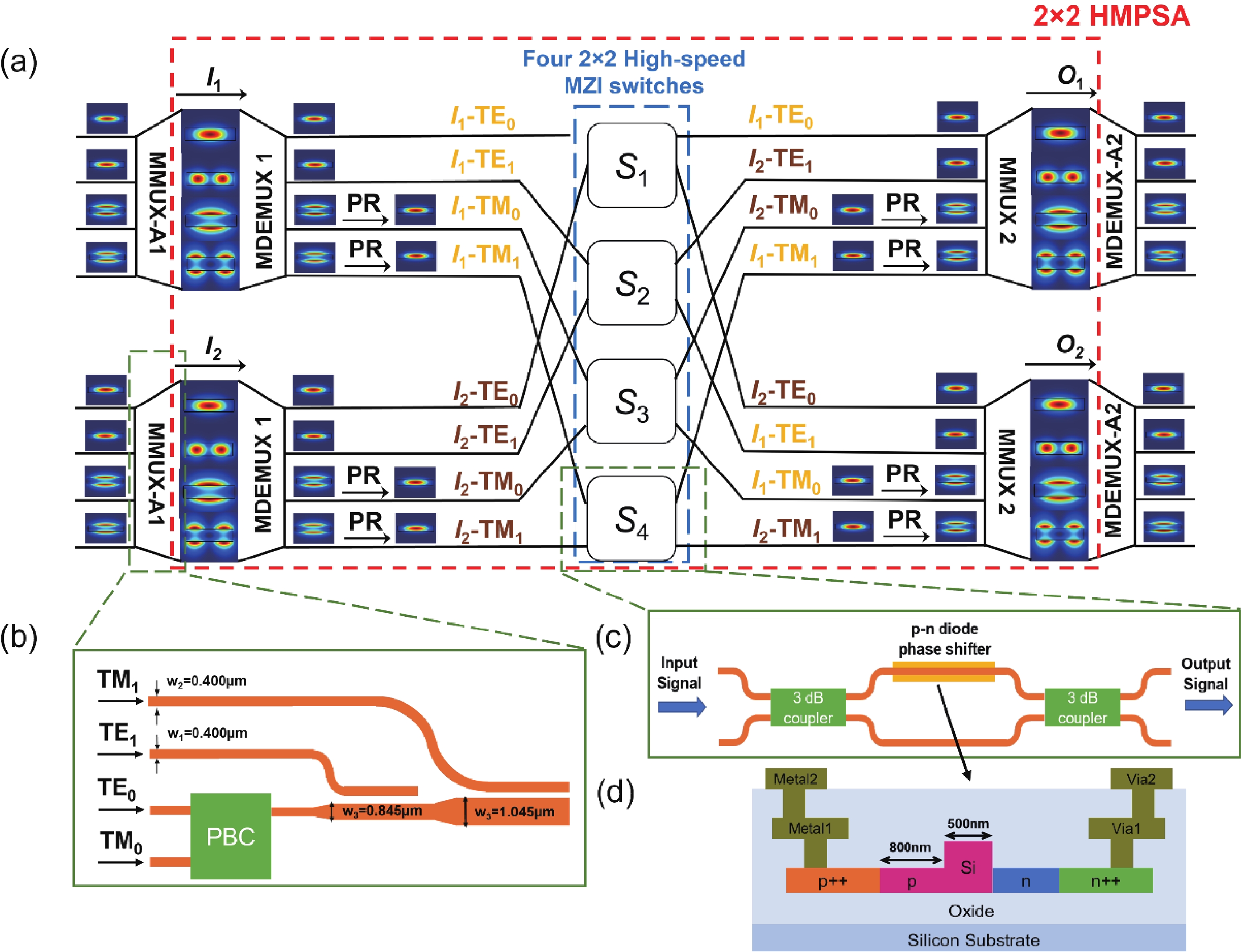
The architecture of the silicon-integrated HMPSA for two modes and dual polarizations is shown in Fig. 1(a). Similarly to a wavelength switch-and-selector architecture, the HMPSA can route any optical signal from one input port to an arbitrary output port.
![]()
Figure 1.(Color online) (a) Architecture of the proposed 2 × 2 HMPSA (The calculated mode patterns of the TE0, TE1, TM0 and TM1 modes are intensity profiles). Structures of (b) MMUX and (c) 2 × 2 high-speed MZI switch. (d) Cross-sectional view of the PN phase shifter. (MMUX-A: auxiliary mode multiplexer; MDEMUX-A: auxiliary mode de-multiplexer.)
The proposed switches consist of mode polarization beam splitters (PBSs), mode multiplexers (MMUXs), polarization rotators (PRs) and crossings. The mode multiplexers are based on asymmetric directional couplers to multiplex the TE1 and TM1 modes[
Various structures have been used as MMUX, such as Y-splitters[
Fig. 1(c) depicts the schematic configuration of the 2 × 2 high-speed MZI switch. A 2 × 2 MMI structure is used as the 3 dB coupler for its compact size and broad-band response. One arm of the MZI contains an EO phase shifter based on a lateral 50-μm-long p–n diode to induce the π phase shift for high-speed switching operations.
3. Fabrication and results
The fabrication of the HMPSA chip is carried out by ultra-violet lithography on a silicon-on-insulator wafer with a 220-nm-thick silicon layer on 2 µm buried dioxide layer using CMOS processes in AMF, Singapore. Fig. 2(a) shows the micrograph of the fabricated 2 × 2 HMPSA with a footprint of 2.2 × 0.9 mm2. Fig. 2(b)–2(e) depict magnified micrographs of a PBS, a MMUX, a PR, a 2 × 2 high-speed MZI switch and waveguide crossings, respectively.
![]()
Figure 2.(Color online) (a) Micrograph of a silicon chip including a HMPSA. Magnified micrographs of (b) a PBS and a MMUX, (c) a PR, (d) a MZI switch and (e) waveguide crossings.
In the experiment setup, a tunable light source (Keysight 81960A) and an optical power meter (Keysight N7744A) are utilized to measure the spectral responses of the HMPSA. Light is coupled into and out of the HMPSA by grating couplers with a shallow etching depth of 70 nm and periods of 630 and 980 nm for supporting TE and TM polarization, respectively. The fiber-to-chip coupling losses are 5.3 and 6.4 dB/facet at 1550 nm, respectively. Fig. 3 shows the measured transmission spectra, which have been normalized by the grating couplers and the MMUX on the same chip. Table 1 summarizes the ILs performance of the building blocks. Take the input port I1 of TE0 channel as an example. When the powers supplied to the heater are 6.23 and 29.03 mW, the signals are switched to output port O1 and O2, respectively. By tuning the powers applied to the corresponding MZI switches, optical signal from each input port is capable of being routed to all available output ports for all the channels. Here we manually adjusted the switching power to allow the maximum output optical power, while it is possible to achieve switch control and calibration with built-in power monitors and a feedback loop[
![]()
Figure 3.(Color online) Results of measured inter-modal crosstalk.
Table Infomation Is Not EnableFig. 4 shows the measured intra-modal XT introduced by the high-speed MZI switches. For the port I1-TE0, the measured intra-modal XT are below –10.13 dB at 1550 nm. For all the inputs, the overall intra-modal XT are lower than –7.32 dB at 1550 nm. The relatively large crosstalk introduces significant, but tolerable, impairments for a quadrature phase-shift keying (QPSK) format by using an on-chip self-homodyne coherent detection scheme[
![]()
Figure 4.(Color online) Results of measured intra-modal crosstalk.
We then measure the dynamic routing performance of the switch by applying a 1 MHz square-wave voltage signal to the device. The peak-to-peak drive voltage is 1.1 V biased at a direct current voltage at 0.8 V. Fig. 5 shows the measured response for the switch. The measured 10%–90% switching time upon electrical tuning are 11 and 10 ns for the rising and falling edges, respectively.
![]()
Figure 5.(Color online) Measured dynamic response of the switch. Yellow and blue curves represent the applied square-wave voltage signal and measured signal dynamic switching, respectively. The dotted lines donate the 10% and 90% of the peak voltage.
4. Conclusion
In conclusion, a 2 × 2 HMPSA is experimentally demonstrated based on EO MZIs. The ILs of the switch are 3.55–9.03 dB at 1550 nm. The measured inter-modal and intra-modal XT values are better than –15.86 and –7.32 dB at 1550 nm, respectively. The switching time (10%–90%) for the rising and falling edges are 11 and 10 ns, respectively. The demonstrated silicon 2 × 2 HMPSA has promising potential for future high-speed optical networks with switching time of only nanoseconds. Furthermore, this scheme can be extended to higher-order modes by employing cascaded subwavelength-grating-based directional couplers[
Acknowledgements
This work was supported in part by the National Key Research and Development Program of China under Grant 2019YFB2203600, the National Natural Science Foundation of China (NSFC) under Grant 61975115/61835008/62035016, and the Science and Technology Commission of Shanghai Municipality under Grant 2017SHZDZX03.
References
[1] P J Winzer, D T Neilson, A R Chraplyvy. Fiber-optic transmission and networking: The previous 20 and the next 20 years. Opt Express, 26, 24190(2018).
[2] B Stern, X L Zhu, C P Chen et al. On-chip mode-division multiplexing switch. Optica, 2, 530(2015).
[3] Y L Xiong, R B Priti, O Liboiron-Ladouceur. High-speed two-mode switch for mode-division multiplexing optical networks. Optica, 4, 1098(2017).
[4] Y H Yao, Z Cheng, J J Dong et al. Performance of integrated optical switches based on 2D materials and beyond. Front Optoelectron, 13, 129(2020).
[5] Y H Zhao, X Wang, D S Gao et al. On-chip programmable pulse processor employing cascaded MZI-MRR structure. Front Optoelectron, 12, 148(2019).
[6] Y K Su, Y Zhang, C Y Qiu et al. Silicon photonic platform for passive waveguide devices: Materials, fabrication, and applications. Adv Mater Technol, 5, 1901153(2020).
[7] L W Luo, N Ophir, C P Chen et al. WDM-compatible mode-division multiplexing on a silicon chip. Nat Commun, 5, 3069(2014).
[8] H Jia, S L Yang, T Zhou et al. WDM-compatible multimode optical switching system-on-chip. Nanophotonics, 8, 889(2019).
[9] L S Han, B P P Kuo, N Alic et al. Silicon Photonic Wavelength and Mode Selective Switch for WDM-MDM networks. 2019 Optical Fiber Communication Conference (OFC), 1(2019).
[10] H Jia, T Zhou, L Zhang et al. Optical switch compatible with wavelength division multiplexing and mode division multiplexing for photonic networks-on-chip. Opt Express, 25, 20698(2017).
[11] Y Zhang, Y He, Q M Zhu et al. On-chip silicon photonic 2 × 2 mode- and polarization-selective switch with low inter-modal crosstalk. Photon Res, 5, 521(2017).
[12] Y Zhang, R H Zhang, Q M Zhu et al. Architecture and devices for silicon photonic switching in wavelength, polarization and mode. J Light Technol, 38, 215(2019).
[13] D Dai, J Wang, Y Shi. Silicon mode (de)multiplexer enabling high capacity photonic networks-on-chip with a single-wavelength-carrier light. Opt Lett, 38, 1422(2013).
[14] Y Y Liu, J M Shainline, X G Zeng et al. Ultra-low-loss CMOS-compatible waveguide crossing arrays based on multimode Bloch waves and imaginary coupling. Opt Lett, 39, 335(2014).
[15] S Y Siew, B Li, F Gao et al. Review of silicon photonics technology and platform development. J Light Technol, 39, 4374(2021).
[16] J B Driscoll, R R Grote, B Souhan et al. Asymmetric Y junctions in silicon waveguides for on-chip mode-division multiplexing. Opt Lett, 38, 1854(2013).
[17] W Chen, P Wang, J Yang. Mode multi/demultiplexer based on cascaded asymmetric Y-junctions. Opt Express, 21, 25113(2013).
[18] T Uematsu, Y Ishizaka, Y Kawaguchi et al. Design of a compact two-mode multi/demultiplexer consisting of multimode interference waveguides and a wavelength-insensitive phase shifter for mode-division multiplexing transmission. J Light Technol, 30, 2421(2012).
[19] Y Sun, Y L Xiong, W N Ye. Experimental demonstration of a two-mode (de)multiplexer based on a taper-etched directional coupler. Opt Lett, 41, 3743(2016).
[20] H Jia, L Zhang, J Ding et al. Microring modulator matrix integrated with mode multiplexer and de-multiplexer for on-chip optical interconnect. Opt Express, 25, 422(2017).
[21] D Dai, M Mao. Mode converter based on an inverse taper for multimode silicon nanophotonic integrated circuits. Opt Express, 23, 28376(2015).
[22] W F Jiang, J Y Miao, T Li. Compact silicon 10-mode multi/demultiplexer for hybrid mode- and polarisation-division multiplexing system. Sci Rep, 9, 13223(2019).
[23] Y Zhang, Y He, H W Wang et al. Ultra-broadband mode size converter using on-chip metamaterial-based Luneburg lens. ACS Photonics, 8, 202(2021).
[24] X Zheng, E Chang, P Amberg et al. A high-speed, tunable silicon photonic ring modulator integrated with ultra-efficient active wavelength control. Opt Express, 22, 12628(2014).
[25] H Jayatilleka, K Murray, M Á Guillén-Torres et al. Wavelength tuning and stabilization of microring-based filters using silicon in-resonator photoconductive heaters. Opt Express, 23, 25084(2015).
[26] D X Dai, C L Li, S P Wang et al. 10-channel mode (de)multiplexer with dual polarizations. Laser Photonics Rev, 12, 1700109(2018).
[27] D X Xu, J H Schmid, G T Reed et al. Silicon photonic integration platform — have we found the sweet spot. IEEE J Sel Top Quantum Electron, 20, 189(2014).
[28] H Z Huang, Y T Huang, Y He et al. Demonstration of terabit coherent on-chip optical interconnects employing mode-division multiplexing. Opt Lett, 46, 2292(2021).
[29] M Okuno, K Kato, R Nagase et al. Silica-based 8 × 8 optical matrix switch integrating new switching units with large fabrication tolerance. J Light Technol, 17, 771(1999).
[30] K Suzuki, G Cong, K Tanizawa et al. Ultra-high-extinction-ratio 2 × 2 silicon optical switch with variable splitter. Opt Express, 23, 9086(2015).
[31] Y He, Y Zhang, Q M Zhu et al. Silicon high-order mode (de)multiplexer on single polarization. J Light Technol, 36, 5746(2018).


Set citation alerts for the article
Please enter your email address

© Copyright 2018-2021 | Chinese Laser Press. All Rights Reserved 沪ICP备15018463号-20