• Journal of the European Optical Society-Rapid Publications
  • Vol. 18, Issue 1, 2022003 (2022)
Heike Müller1、*, Thomas Waak2, Uwe Birnbaum2, Georg Böhm1, and Thomas Arnold1、3
Author Affiliations
  • 1Leibniz Institute of Surface Engineering (IOM), Permoserstraße 15, 04318 Leipzig, Germany
  • 2JENOPTIK Optical Systems GmbH, Göschwitzer Straße 25, 07745 Jena, Germany
  • 3Institute of Manufacturing Science and Engineering, TU Dresden, 01062 Dresden, Germany
  • show less
    DOI: 10.1051/jeos/2022003 Cite this Article
    Heike Müller, Thomas Waak, Uwe Birnbaum, Georg Böhm, Thomas Arnold. Atmospheric Plasma Jet processing for figure error correction of an optical element made from S-BSL7[J]. Journal of the European Optical Society-Rapid Publications, 2022, 18(1): 2022003 Copy Citation Text show less
    Schematic drawing of PJ source.
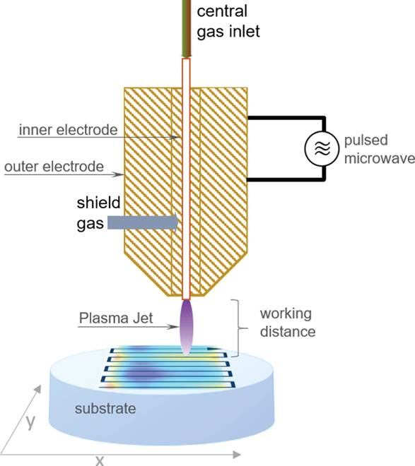
    Fig. 1. Schematic drawing of PJ source.
    Cross-section of the optical element with indication of the main dimensions.
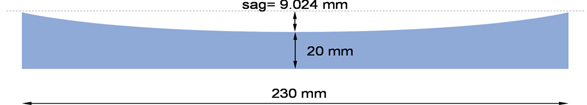
    Fig. 2. Cross-section of the optical element with indication of the main dimensions.
    Measurement of the S-like step after etching semicircle area for computation of the PJ etching parameters.
    Fig. 3. Measurement of the S-like step after etching semicircle area for computation of the PJ etching parameters.
    Influence of different heater temperatures: (a) velocity dependent material removal rate, (b) normalized MRR at different surface temperatures TS, the encircled outliers were not regarded in the linear fit, (c) roughness Sq, (d) birefringence specified as normalized optical path difference and (e) surface topographies representing various surface roughness due to increasing etching depths (TH = 500 °C).
    Fig. 4. Influence of different heater temperatures: (a) velocity dependent material removal rate, (b) normalized MRR at different surface temperatures TS, the encircled outliers were not regarded in the linear fit, (c) roughness Sq, (d) birefringence specified as normalized optical path difference and (e) surface topographies representing various surface roughness due to increasing etching depths (TH = 500 °C).
    (a) Surface temperatures during PJ machining at different velocities applying different microwave power, (b) influence of different microwave power on roughness Sq and (c) birefringence specified as normalized optical path difference.
    Fig. 5. (a) Surface temperatures during PJ machining at different velocities applying different microwave power, (b) influence of different microwave power on roughness Sq and (c) birefringence specified as normalized optical path difference.
    Dependency of MRR normalized to the value at v = 4 mm/s on scan velocity of the PJ having a working distance of 3.5 mm (process parameters: [He] = 200 sccm, [O2] = 2 sccm, [CF4] = 1 sccm, [N2] = 600 sccm, P = 15 W, TH = 500 °C).
    Fig. 6. Dependency of MRR normalized to the value at v = 4 mm/s on scan velocity of the PJ having a working distance of 3.5 mm (process parameters: [He] = 200 sccm, [O2] = 2 sccm, [CF4] = 1 sccm, [N2] = 600 sccm, P = 15 W, TH = 500 °C).
    Figure error correction on optical element: (a) figure error before and (b) after PJ machining, (c) compared to the theoretical figure error resulting from dwell-time calculation.
    Fig. 7. Figure error correction on optical element: (a) figure error before and (b) after PJ machining, (c) compared to the theoretical figure error resulting from dwell-time calculation.
    Isotropic PSD determined at three random points compared to initial surface.
    Fig. 8. Isotropic PSD determined at three random points compared to initial surface.
    Model for thermal FEM simulation: (a) fixation of the sample on mounting plate (yz view), (b) comparison of measured and simulated heating-up curves for different x positions on the optical element, (c) stationary temperature distribution after t = 2100 s.
    Fig. 9. Model for thermal FEM simulation: (a) fixation of the sample on mounting plate (yz view), (b) comparison of measured and simulated heating-up curves for different x positions on the optical element, (c) stationary temperature distribution after t = 2100 s.
    Influence of different surface temperatures on (a) MRR and (b) isotropic PSD (process parameters: 15 W, v = 4 mm/s).
    Fig. 10. Influence of different surface temperatures on (a) MRR and (b) isotropic PSD (process parameters: 15 W, v = 4 mm/s).
    Scaling of the MRR for dwell time calculation as a function of temperature resulting from geometry of the optical element.
    Fig. 11. Scaling of the MRR for dwell time calculation as a function of temperature resulting from geometry of the optical element.
    Figure error of the optical element over the entire processing area (a) before PJM with (b) footprint profile (cross section of line etching for one line, v = 1 mm/s) and (c) figure error after PJM.
    Fig. 12. Figure error of the optical element over the entire processing area (a) before PJM with (b) footprint profile (cross section of line etching for one line, v = 1 mm/s) and (c) figure error after PJM.
    Figure error correction of an optical element: isotropic PSD for defined points on the processed sample.
    Fig. 13. Figure error correction of an optical element: isotropic PSD for defined points on the processed sample.
    Measurement of figure error of the optical element (a) before and (b) after the second PJ correction step and (c) calculation of the isotropic PSD for defined three well-chosen positions on the processed sample.
    Fig. 14. Measurement of figure error of the optical element (a) before and (b) after the second PJ correction step and (c) calculation of the isotropic PSD for defined three well-chosen positions on the processed sample.
    ComponentProportion (%)Chemical reactionBoiling points
    SiO260–70SiO2 + CF4 → SiF4 + CO2−95.2 °C subl. [13]
    B2O310–202B2O3 + 3CF4 → 4BF3 + 3CO2−101 °C [14]
    BaO0–22BaO + CF4 → 2BaF2 + CO22260 °C [14]
    ZnO0–22ZnO + CF4 → 2ZnF2 + CO21500 °C [14]
    Sb2O30–22Sb2O3 +3 CF4 → 4SbF3 + 3CO2345 °C [14]
    Sb2O3 + CF4 + 8F → SbF5 + CO2141 °C [14]
    TiO20–2TiO2 + CF4 → TiF4 + CO2284 °C subl. [14]
    TiO2 + CF4 → TiF3 + CO2 + F1400 °C [14]
    Table 0. Chemical equations and boiling points of the alkalifluorides occuring while plasma etching of BCG with CF4.
    Heater temperature TH (°C)Surface temperature TS (°C)
    400275
    500325
    600370
    Table 0. Indication of the surface temperatures resulting from the preset heater temperatures without heat impact of the PJ.
    ComponentProportion of S-BSL7 (%) (Ohara GmbH)Proportion of N-BK7® (%) (Schott AG)
    SiO260–7060–70
    B2O310–2010–20
    BaO0–21–10
    ZnO0–2
    Sb2O30–2<1
    TiO20–2<1
    Na2O10–20
    K2O1–10
    CaO<1
    Cl2<1
    Table 0. Nominal chemical composition of S-BSL7 compared to N-BK7®.
    Heike Müller, Thomas Waak, Uwe Birnbaum, Georg Böhm, Thomas Arnold. Atmospheric Plasma Jet processing for figure error correction of an optical element made from S-BSL7[J]. Journal of the European Optical Society-Rapid Publications, 2022, 18(1): 2022003
    Download Citation