
Heike Müller, Thomas Waak, Uwe Birnbaum, Georg Böhm, Thomas Arnold. Atmospheric Plasma Jet processing for figure error correction of an optical element made from S-BSL7[J]. Journal of the European Optical Society-Rapid Publications, 2022, 18(1): 2022003
Journals >Journal of the European Optical Society-Rapid Publications >Volume 18 >Issue 1 >Page 2022003 > Article
- Journal of the European Optical Society-Rapid Publications
- Vol. 18, Issue 1, 2022003 (2022)
Abstract
Keywords
List of abbreviations
1 Introduction
An increasing automation of everyday processes requires further development of numerous optical devices, such as those needed for machine vision and laser technology. Human-machine interaction requires the ability of machines to visually record complex scenarios. Metrology is playing an increasingly important role in process monitoring and final inspection. Light is becoming a tool that is of great assistance in autonomous driving [
IOM has a high expertise in the field of ultra-precision figuring with plasmas and ions. Plasma Jet Machining (PJM) is a well-established technique for figuring and correcting various optical lens designs, such as spherical, aspherical and freeform lenses. The material variety, mainly based on silicon, for instance Si, Fused Silica or SiC, is progressively extended to adapt to the market requirements [
Albeit, due to the chemical interactions between the reactive species generated in the plasma and the substrate material of optical glasses, various effects such as layer formation can occur, which influence the local etch rate and thus lead to inhomogeneous and difficult-to-predict material removal. However, for the application of the dwell time method, the exact knowledge of the local removal rate is crucial. Based on extensive fundamental research on plasma processing of N-BK7® the most famous representative of BCG, the influencing parameters were identified and measures to compensate nonlinear effects were developed [
In the following, the workflow for PJM-based figure error correction of an optical element made of S-BSL7 glass is presented. Since surface temperature plays a major role in the chemically driven plasma etching process which significantly affects material removal rate and surface roughness, a careful assessment of the main influencing parameters or their local distribution functions like local surface temperature and etching rate function depending on substrate heater temperature, natural convection, plasma power, and local dwell time has been undertaken. Such parameters and functions are then introduced into the process simulation in order to calculate local dwell times for the machining process. Preliminary tests show the feasibility of this approach. Finally, the successful correction of an optical element made of S-BSL7, and the achievement of optical surface quality is demonstrated.
2 Experimental
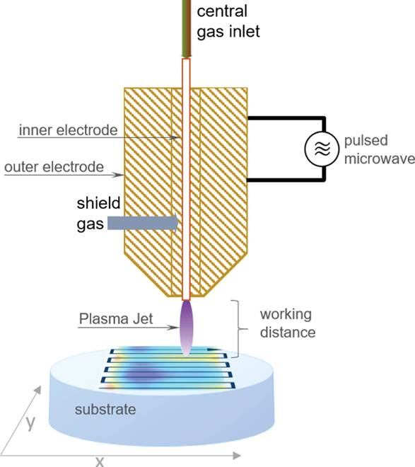
The principle of PJM was developed at the IOM about two decades ago. Since then, the Plasma Jet (PJ) source has been continuously improved to meet current research purposes and material requirements. A schematic drawing of the PJ source used in this work can be seen in
![]()
Figure 1.Schematic drawing of PJ source.
A microwave generator (PP3030, Trionplas Technologies GmbH) coupled via a coaxial cable to the PJ source provides microwave power to plasma nozzle where the gas mixture is excited by a high-frequency electric field. Pulsed microwave of 2.45 GHz with peak power of 250 W, pulse frequency of approx. 1 kHz and pulse length of approx. 10 μs propagates along the inner electrode. A mean power of 10 W to 20 W can be adjusted by varying the pulse frequency. The ignition of the gas discharge at the nozzle tip occurs as soon as the intensity of the electric field intensity exceeds the breakdown intensity and at least one free electron is present. In the excited gas flow, dissociation and recombination of the CF4 molecules occur. The fluorine radicals react with the silicon-containing substrate forming gaseous compounds, which lead to material removal. In the case of Fused Silica (SiO2), only volatile components such as SiF4 and CO2 are formed. For substrates containing additional components like BCG, individual considerations of their surface reactions must be made, as further glass constituents strongly influence the etching behavior during plasma jet processing.
3 Material and measurements
Due to their low refractive index (ne = 1.52) and low dispersion (νe = 63.93), crown glasses are commonly used for optical elements applied in visible and near-infrared spectra. BCG is defined as a type of crown glasses consisting of approx. 60–70% SiO2 and at least 10% of boron oxide among other metal oxide constituents. As a result, such glasses are characterized by high mechanical hardness and chemical resistance. Several fundamental studies on the plasma jet figuring of N-BK7® made by Schott AG have been performed in recent years [
Since the various BCG differ slightly in their composition the investigations of N-BK7® cannot be fully used for the processing of S-BSL7 glass. Minor adjustments in etching behavior are to be expected due to the variation of the components. {L-End}
It was shown that PJ etching of BCG using fluorine-containing gas, such as CF4, results in the formation of fluorides. Their individual boiling point determines whether the reaction products form volatile compounds or solid material. The chemical equations and boiling points of the components involved can be found in
The dimensions of the optical element made from S-BSL7 which is to be corrected are shown in
![]()
Figure 2.Cross-section of the optical element with indication of the main dimensions.
Etching tests prior to the processing of the optical element were performed on smaller round S-BSL7 glass samples with a diameter of 18 mm and a thickness of 9 mm exhibiting a planar polished surface. With these test samples the plasma process parameters were optimized and the effects of the PJ scan velocity and local surface temperatures on the etching rate were investigated.
In order to remove any surface contamination or particles that could affect the etching results, the samples were cleaned in an ultrasonic bath prior to processing. After PJ etching, the samples were cooled slowly. Then again, they were ultrasonic cleaned to remove the residual layer before performing surface measurements.
For PJM the test samples as well as the optical element are placed on a substrate heater in the CNC machine which enables to heat up the glass substrates to temperatures up to 600 °C.
The heating and cooling behavior of the samples were determined by IR-thermography using an IR camera (PI160, Optris GmbH) mounted on the motion system. This camera is pointed at the contact zone of the PJ and the substrate. Furthermore, the camera is installed in such a way on the motion system that it follows the line feed in the y-direction. In x-direction, the PJ passes through the measuring point when executing a line scan. Thus, in addition to the determination of the temporal trend of the full sample surface heating during processing the current temperature in the contact zone could be observed. The emissivity of the glass substrate was adjusted to ε = 0.8 by temperature comparison of a sooted and a bare glass surface where the emissivity on the sooted area was assumed to be ε = 0.95 [
To determine the material removal of the round test samples, the processed substrates were measured using a non-contact optical surface profiler (LuphoScan 260HD, Taylor Hobson Ltd.). By deconvolution of the S-like step (see
![]()
Figure 3.Measurement of the S-like step after etching semicircle area for computation of the PJ etching parameters.
The figure error of the optical element was determined based on an area measurement using the non-contact profilometer (CT350S, Cyber Technologies GmbH). By matching with the nominal surface design, the figure error was calculated.
Surface roughness was evaluated by White Light Interferometry (WLI, NPFLEX, Bruker Corporation) using different objectives. With the help of a Matlab® script, a combined isotropic Power Spectral Density (PSD) function was calculated from the individual measurements covering a total spatial wavelength range of approx. 1.1 × 10⁻³ μm−1 to 2 μm−1.
The occurrence of birefringence induced by internal stress was observed using the StrainScope S3/180 (ilis GmbH). In accordance with the conventions of optical technologies, the values of the Optical Path Difference (OPD) were normalized to the thickness of the samples.
To determine the basic etching behavior, five test samples were evenly distributed on a sample holder, which in turn was positioned on the heater. By arranging those samples, five different scan velocities of the PJ could be tested in one heating cycle. Semicircle areas were etched applying a meander path with constant velocities (1, 2, 4, 8, 16 mm/s). The radius of the area was 10 mm, and the line feed was 0.1 mm.
Figure error correction was performed based on the dwell-time method. The usual mathematical description for the relationship between etching depth, tool function and dwell time can be expressed as follows: hij =R × tij + ε. In order to obtain the dwell time matrix tij, deconvolution of the topography of the figure error, represented by a discrete height matrix hij, with the tool function R approximated by a rotationally symmetric Gaussian function is performed. Additionally, the theoretical residual error ε is obtained. For the purpose of PJ etching a dedicated numerical deconvolution algorithm was employed over the last decades. Besides other specific features it is able to account for variable local etch rates. Finally, the dwell time matrix tij is transferred to local velocities, considering the tool path and the machine kinematics, and provided as CNC data for machining.
4 Results
4.1 Optimization of etching behavior of S-BSL7
For a successful application of PJM on S-BSL7 process parameters have to be optimized in terms of maximum material removal rate, minimum surface roughness, and minimum birefringence ensuring minimum processing time and high optical performance of the optical element. In order to investigate the etching behavior of the substrate material S-BSL7, first the influence of the surface temperature is considered, which is mainly achieved by external sample heating.
Kazemi et al. investigated the influence of surface temperature in detail [
The surface temperatures result from the equilibrium of heat flow from the sample heater as heat source and natural convection of ambient air as heat sink. For these measurements, the PJ was not yet in contact with the sample surface.
For the determination of the material removal rate depending on different surface temperatures as well as for varying scan velocities of the plasma jet the microwave power was set to 10 W. The central gas inlet was fed by [He] = 200 sccm He, [O2] = 2 sccm O2 and [CF4] = 1 sccm CF4. The outer shield gas flow rate was adjusted to [N2] = 600 sccm N2. The results are shown in
![]()
Figure 4.Influence of different heater temperatures: (a) velocity dependent material removal rate, (b) normalized MRR at different surface temperatures TS, the encircled outliers were not regarded in the linear fit, (c) roughness Sq, (d) birefringence specified as normalized optical path difference and (e) surface topographies representing various surface roughness due to increasing etching depths (TH = 500 °C).
It is well known that the chemical reaction rates on the surface are mainly controlled by the Arrhenius law, which can be described by
It has been shown in previous plasma jet related work [
In order to evaluate the surface quality after etching, surface roughness was measured. The results are shown in
Consequently, it can be concluded that the temperature of the heater should be selected high enough to enable low roughness. Here, however, the glass transition temperature has to be considered, which is TG = 576 °C for S-BSL7. Even if the temperature does not reach this value at the surface, higher temperatures are achieved in direct contact between the sample backside and the aluminum holder. Nonuniform heating of the glass can lead to birefringence which may deteriorate the optical performance of optics. Looking at the birefringence shown in
Based on the results obtained so far, a heater temperature of TH = 500 °C (i.e. a global surface temperature of TS = 325 °C) was used to perform further investigations on the influence of applied microwave power. For these tests, mean power levels of 12 W and 15 W were adjusted to compare the etching results with those obtained at 10 W using the same experimental setup. In order to better assess the effect of increasing microwave power, local surface temperatures during processing were measured, which are depicted in
![]()
Figure 5.(a) Surface temperatures during PJ machining at different velocities applying different microwave power, (b) influence of different microwave power on roughness Sq and (c) birefringence specified as normalized optical path difference.
The roughness Sq, measured with the 50× objective, shows a nearly linear dependence on the resulting etching depth for 10 W (see
The investigations show that for a power level of 15 W a reasonable roughness and no significant rise of birefringence is obtained. Hence, the following dwell time-controlled figure error correction process is performed at the power level of 15 W and 500 °C heater temperature.
4.2 Figure error correction on optical element
A first figure error correction test was performed on a partial area of a test substrate heated to TH = 500 °C with the dimensions of the optical component shown in
The global surface temperature TS measured with the IR camera is between 300 °C and 325 °C. To take the velocity dependence of the MRR into account, the normalized etching rates given in
![]()
Figure 6.Dependency of MRR normalized to the value at v = 4 mm/s on scan velocity of the PJ having a working distance of 3.5 mm (process parameters: [He] = 200 sccm, [O2] = 2 sccm, [CF4] = 1 sccm, [N2] = 600 sccm, P = 15 W, TH = 500 °C).
![]()
Figure 7.Figure error correction on optical element: (a) figure error before and (b) after PJ machining, (c) compared to the theoretical figure error resulting from dwell-time calculation.
To determine the roughness, the sample was measured by WLI at three random measurement points after correction.
![]()
Figure 8.Isotropic PSD determined at three random points compared to initial surface.
Although the previous result is promising, a measurement of the surface temperature of the entire surface of the optical element reveals a non-uniform temperature distribution. This lateral distribution must be additionally considered in the dwell time calculation when the full surface is to be processed, as it influences the MRR. A characteristic local temperature distribution originates from the dimensions of the heater and the workpiece holder setup. The optical element is mounted in a fixed position on the heater by using a sample holder. The combination of optics and mounting plate is shown in
![]()
Figure 9.Model for thermal FEM simulation: (a) fixation of the sample on mounting plate (yz view), (b) comparison of measured and simulated heating-up curves for different x positions on the optical element, (c) stationary temperature distribution after t = 2100 s.
Since the IR camera measurements on the curved surface are only estimates and may contain measurement errors due to varying angle of incidence the temperature of the sample surface was modeled using COMSOL® Multiphysics. The measured heater temperature (TH = 500 °C) is taken as one boundary condition. Furthermore, convective cooling by the surrounding air is assumed. According to the real conditions, the bottom of the sample is in full contact with the sample holder, while are narrow air gaps of 0.1 mm are considered between the side walls and the sample.
In
A stationary temperature distribution shown in
A quantitative determination of the MRR depending on the surface temperature was performed on three test samples. Different surface temperatures (approximately: TS = 245 °C/290 °C/340 °C) were adjusted to reflect the conditions of the optical element at different lateral positions.
![]()
Figure 10.Influence of different surface temperatures on (a) MRR and (b) isotropic PSD (process parameters: 15 W, v = 4 mm/s).
In addition, the isotropic PSD compared to the initial surface for all three surface temperatures is given in
Based on the previous results, the MRR is adjusted according to the temperatures resulting from the FEM simulation due to the geometry of the optical element. The normalized MRR, which is shown in
![]()
Figure 11.Scaling of the MRR for dwell time calculation as a function of temperature resulting from geometry of the optical element.
Comparing the influences of both dependencies the non-uniform sample heating is more influential and leads to a reduction of the MRR of 25%. The velocity, on the other hand, causes the MRR to vary by only about ±3%, so its influence is comparatively small but nevertheless of importance not to be underestimated in high-precision figure error correction. Based on a surface form measurement, a figure error correction of the optical element was performed. The initial figure error is shown in
![]()
Figure 12.Figure error of the optical element over the entire processing area (a) before PJM with (b) footprint profile (cross section of line etching for one line, v = 1 mm/s) and (c) figure error after PJM.
The dwell time calculation results in a process time of about 3 h. During processing, the heater temperature was TH = 500 °C. The plasma jet (see footprint profile in
Roughness measurements and the derived isotropic PSD function at different positions on the surface shown in
![]()
Figure 13.Figure error correction of an optical element: isotropic PSD for defined points on the processed sample.
However, when looking at the roughness at about x = ±100 mm, there are significant differences. The removal depth which influences the roughness, as shown in
Due to the increased roughness after the figure error correction an additional mechanical-abrasive sub-aperture polishing step was required. The surface error increased from rms = 115.8 nm to rms = 351.5 nm, as can be seen in
![]()
Figure 14.Measurement of figure error of the optical element (a) before and (b) after the second PJ correction step and (c) calculation of the isotropic PSD for defined three well-chosen positions on the processed sample.
A second PJM step was subsequently performed to further reduce form error using the same dwell time correction procedure as previously described. Hereby, the figure error was further decreased. To counteract the non-uniform global heating of the sample due to the heat input from the PJ, the line feed was performed here along the y direction. An areal measurement of the figure error after PJ processing is shown in
The roughness shown as isotropic PSD in
5 Conclusion
PJM to correct surface figure error of an optical element made of S-BSL7 was investigated. It was shown that the surface temperature has a significant effect on the MRR. In order to perform a deterministic correction process, the nonlinear dependence of motion velocity of the plasma jet as well as the characteristic surface temperature distribution on the MRR must be taken into account for the dwell time calculation. It has been demonstrated that figure error of an S-BSL7 optical element can be reduced by up to 74%. A global surface temperature of about 325 °C to 350 °C leads to a stable PJ etching process resulting in a uniform surface roughness. However, surface temperature below 300 °C leads to higher roughness. Consequently, more uniform heating of the substrate while maintaining the optimum surface temperature, e.g. by an optimized configuration of substrate heating, should be considered in future. Due to the increased surface roughness of the PJ processed surface, subsequent mechanical polishing is required. Minimizing the surface roughness reduces the polishing effort and results in less figure deterioration. Depending on the magnitude of initial figure error, iterative processing is proposed, including multiple cycles of PJM and polishing or smoothing.
References
[1] L. Fischer, D. Holder, S. Krogmann, T. Maier. Integration von Sensoren in das Exterieur-Design automatisierter/autonomer Fahrzeuge, 13(2021).
[2] VDI . Automatisiertes und autonomes Fahren (VDI-Handlungsempfehlung)(2019).
[3] SPECTARIS-Fachverband Photonik . Trendreport Photonik 2019/2020 – Märkte, Entwicklungen, Potenziale(2019).
[4] J.P. Rolland, M.A. Davies, T.J. Suleski, C. Evans, A. Bauer, J.C. Lambropoulos, K. Falaggis. Freeform optics for imaging.
[5] V.V. Yashchuk, S. Rochester, I. Lacey, S. Babin. Super-resolution surface slope metrology of X-ray mirrors.
[6] F. Kazemi, G. Boehm, T. Arnold. A novel Deal–Grove-inspired model for fluorine-based plasma jet etching of borosilicate crown optical glass.
[7] F. Kazemi, G. Boehm, T. Arnold. Recursive algorithm for modeling non-linear etching rates in reactive plasma jet based optical surface machining of borosilicate crown glass.
[8] C.J. Mogab, A.C. Adams, D.L. Flamm. Plasma etching of Si and SiO2 – The effect of oxygen additions to CF4 plasmas.
[9] F. Kazemi, G. Boehm, T. Arnold. Development of a model for ultra-precise surface machining of N-BK7® using microwave-driven reactive plasma jet machining.
[10] F. Kazemi, G. Boehm, T. Arnold. An investigation on effectiveness of temperature treatment for fluorine-based reactive plasma jet machining of N-BK7®.
[11] OHARA GmbH OHARA.
[12] AG Schott.
[13] N. Wiberg. Lehrbuch der anorganischen Chemie(2008).
[14] D.R. Lide.
[15] J.H. Lienhard, J.H. Lienhard.
[16] Th Arnold, G. Böhm, H. Paetzelt. Ultra-precision surface machining with reactive plasma jets: ultra-precision surface machining with reactive plasma jets.
[17] X. Su, P. Ji, Y. Jin, D. Li, Z. Qiao, F. Ding, X. Yue, B. Wang. Freeform surface generation by atmospheric pressure plasma processing using a time-variant influence function.
[18] T. Arnold, G. Boehm, I.-M. Eichentopf, M. Janietz, J. Meister, A. Schindler. Plasma Jet Machining: A novel technology for precision machining of optical elements.
[19] J. Meister, T. Arnold. New process simulation procedure for high-rate plasma jet machining.


Set citation alerts for the article
Please enter your email address

© Copyright 2018-2021 | Chinese Laser Press. All Rights Reserved 沪ICP备15018463号-20