Sihao Huang, Zhengzheng Liu, Juan Du, Yuxin Leng. Review of Perovskite Micro -and Nano-Lasers[J]. Laser & Optoelectronics Progress, 2020, 57(7): 071602
Search by keywords or author
- Laser & Optoelectronics Progress
- Vol. 57, Issue 7, 071602 (2020)
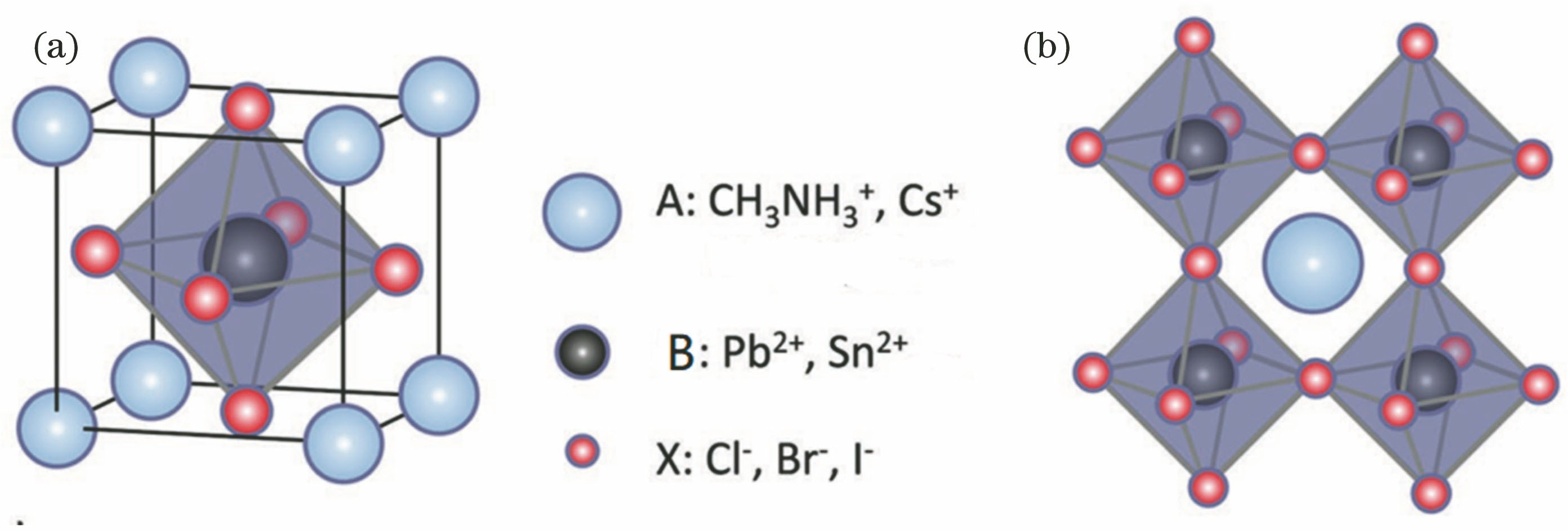
![Perovskite crystal structure[22]. (a) Perovskite cell structure; (b) general ABX3 perovskite 3D crystal structure](/richHtml/lop/2020/57/7/071602/img_1.jpg)
Fig. 1. Perovskite crystal structure[22]. (a) Perovskite cell structure; (b) general ABX3 perovskite 3D crystal structure
![Wavelength tunability of perovskite nanomaterials. (a) By changing the ratio of iodine to bromine in MAPb(I1-xBrx)3, tuning of 786 to 544 nm can be achieved. Above is the absorption spectrum, below is an image of the nanocomposite[40]; (b) MAPbX3(X=Cl, Br, I) can be tuned to the emission wavelength from 390 to 790 nm in visible infrared by changing the ratio of hal](/richHtml/lop/2020/57/7/071602/img_2.jpg)
Fig. 2. Wavelength tunability of perovskite nanomaterials. (a) By changing the ratio of iodine to bromine in MAPb(I1-xBrx)3, tuning of 786 to 544 nm can be achieved. Above is the absorption spectrum, below is an image of the nanocomposite[40]; (b) MAPbX3(X=Cl, Br, I) can be tuned to the emission wavelength from 390 to 790 nm in visible infrared by changing the ratio of hal
Fig. 3. Organo-inorganic hybrid perovskite WGM laser. (a) Near-infrared WGM laser for hexagonal and triangular perovskite MAPbI3-aXa nanocrystals[59]; (b) quadrilateral perovskite MAPbBr3 nanoplatelet with the increase of pump strength, the appearance of WGM laser and the optical excitation image of nanoplatelet above and below the threshold[60]; (c) WGM
Fig. 4. Different schemes of WGM mode laser. (a) WGM microcavity was formed by cross section of two crossed perovskite MAPbBr3 nanorods[64]; (b) tunable size of the perovskite CsPbX3 nano inorganic spheres WGM microcavity[65]; (c) WGM laser is realized by using silicon sphere as resonator[35]; (d) WGM mode laser is implemented
Fig. 5. Different schemes of WGM mode laser. (a) Schemes of inorganic perovskite CsPbBr3 quantum dots embedded silica sphere[72]; (b) CsPbBr3-SiO2 micro sphere into a diameter of 40 μm cylindrical tubes of luminous images, and the principle of laser WGM mode[72]; (c) CdS/CsPbBr3 shell/core structure[74]; (d) CsPb
Fig. 6. Perovskite nanowire laser. (a) Scheme of nanowire structure lasers[76-77]; (b) optical image of MAPbX3 perovskite nanowires with increased pump light intensity[44]; (c) with the increase of pumping intensity, intensity distribution of F-P mode perovskite MAPbIxCl3-x nanowires laser[![All inorganic perovskite CsPbX3 nanowires. (a) Nanowire lasing image with different pump density[79]; (b) with the increase of excitation intensity, F-P mode laser appears on perovskite CsPbBr3 nanowires[79]; (c) nanowire laser can last for more than an hour (equivalent to 109 excitation cycles) with a fixed pulsed energy[<xref ref-type="bibr" rid="b79"](/Images/icon/loading.gif)
Fig. 7. All inorganic perovskite CsPbX3 nanowires. (a) Nanowire lasing image with different pump density[79]; (b) with the increase of excitation intensity, F-P mode laser appears on perovskite CsPbBr3 nanowires[79]; (c) nanowire laser can last for more than an hour (equivalent to 109 excitation cycles) with a fixed pulsed energy[![Different schemes of F-P mode lasers. (a) F-P mode laser in all inorganic perovskite CsPbBr3 micron cube[86]; (b) SEM image of high-quality perovskite CsPbBr3 nano cubes using an improved low-temperature solution treatment method[87]; (c) schematic of the crystal structure and standing wave of the F-P cavity[87]; (d) inorganic](/Images/icon/loading.gif)
![F-P mode laser with auxiliary cavity. (a) Perovskite MAPbI3-xClx vertical cavity F-P mode laser spectrum[90]; (b) structure of all-inorganic perovskite CsPbBr3 VCSEL[93]; (c) FP mode laser spectrogram[93]; (d) perovskite laser with DFB structure[94](/Images/icon/loading.gif)
![Random lasers. (a) Random lasers using multiple scattering from a disordered medium[96]; (b) fluorescent images showing the pumping intensity, spatial distribution of perovskite MAPbI3 random lasers[97]; (c) emission spectrum diagrams below the pump threshold, close to the pump threshold, and above the pump threshold[97]; (d) TEM image o](/Images/icon/loading.gif)
Fig. 8. Different schemes of F-P mode lasers. (a) F-P mode laser in all inorganic perovskite CsPbBr3 micron cube[86]; (b) SEM image of high-quality perovskite CsPbBr3 nano cubes using an improved low-temperature solution treatment method[87]; (c) schematic of the crystal structure and standing wave of the F-P cavity[87]; (d) inorganic
Fig. 9. F-P mode laser with auxiliary cavity. (a) Perovskite MAPbI3-xClx vertical cavity F-P mode laser spectrum[90]; (b) structure of all-inorganic perovskite CsPbBr3 VCSEL[93]; (c) FP mode laser spectrogram[93]; (d) perovskite laser with DFB structure[94
Fig. 10. Random lasers. (a) Random lasers using multiple scattering from a disordered medium[96]; (b) fluorescent images showing the pumping intensity, spatial distribution of perovskite MAPbI3 random lasers[97]; (c) emission spectrum diagrams below the pump threshold, close to the pump threshold, and above the pump threshold[97]; (d) TEM image o

Set citation alerts for the article
Please enter your email address


