• Photonics Research
  • Vol. 8, Issue 2, 194 (2020)
Jérôme Michon1、*, Sarah Geiger1、2, Lan Li3、4, Claudia Goncalves5, Hongtao Lin6, Kathleen Richardson5, Xinqiao Jia2、7, and Juejun Hu1、8
Author Affiliations
  • 1Department of Materials Science and Engineering, Massachusetts Institute of Technology, Cambridge, Massachusetts 02139, USA
  • 2Department of Biological Engineering, University of Delaware, Newark, Delaware 19716, USA
  • 3Key Laboratory of 3D Micro/Nano Fabrication and Characterization of Zhejiang Province, School of Engineering, Westlake University, Hangzhou 310024, China
  • 4Institute of Advanced Technology, Westlake Institute for Advanced Study, Hangzhou 310024, China
  • 5College of Optics & Photonics, University of Central Florida, Orlando, Florida 32816, USA
  • 6College of Information Science and Electronic Engineering, Zhejiang University, Hangzhou 310027, China
  • 7e-mail: xjia@udel.edu
  • 8e-mail: hujuejun@mit.edu
  • show less
    DOI: 10.1364/PRJ.375584 Cite this Article Set citation alerts
    Jérôme Michon, Sarah Geiger, Lan Li, Claudia Goncalves, Hongtao Lin, Kathleen Richardson, Xinqiao Jia, Juejun Hu. 3D integrated photonics platform with deterministic geometry control[J]. Photonics Research, 2020, 8(2): 194 Copy Citation Text show less
    (a) Schematic of the proposed 3D fabrication process. (b) Schematic of the 3D device layout.
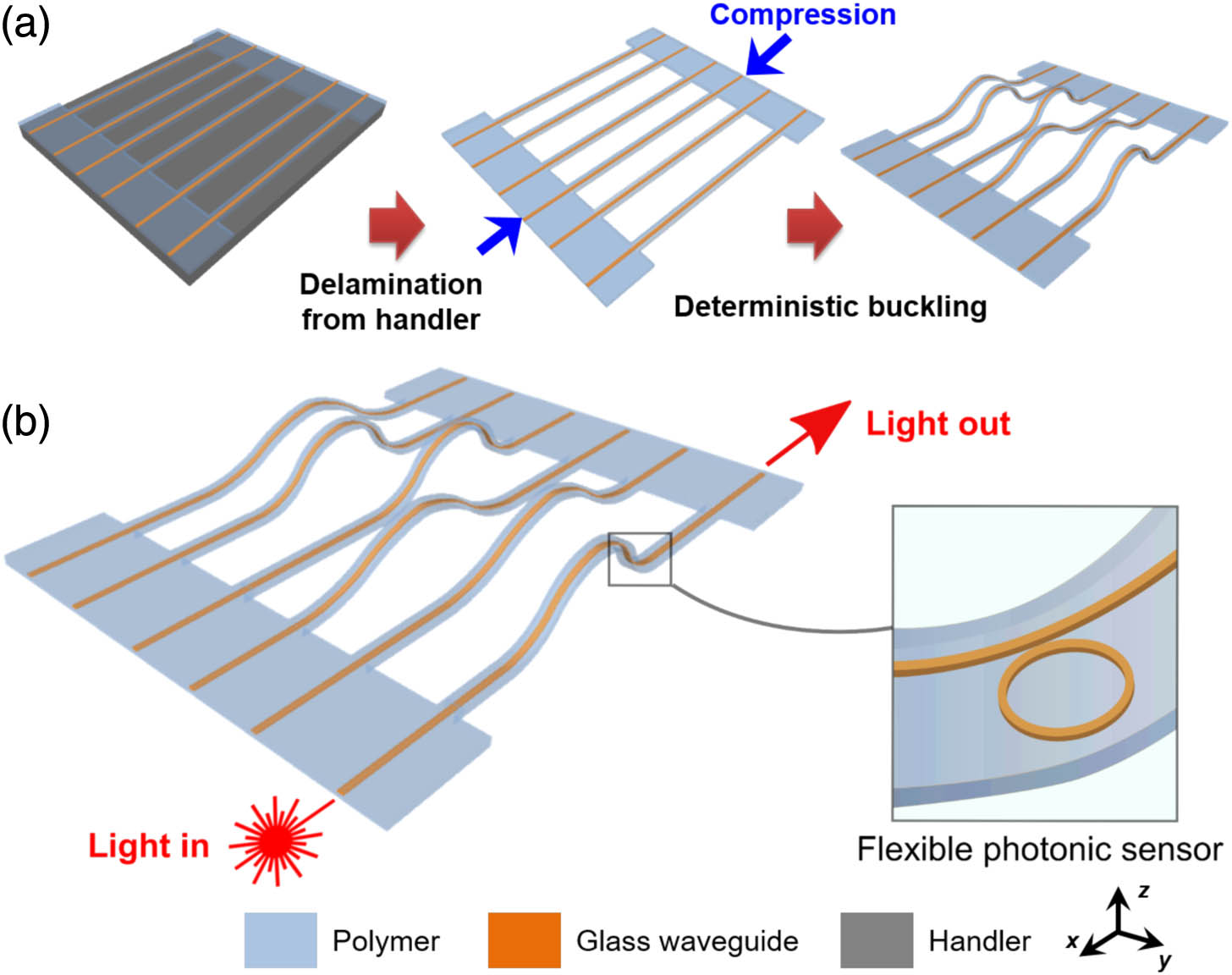
    Fig. 1. (a) Schematic of the proposed 3D fabrication process. (b) Schematic of the 3D device layout.
    Overall fabrication process flow of the 3D integrated photonics devices.
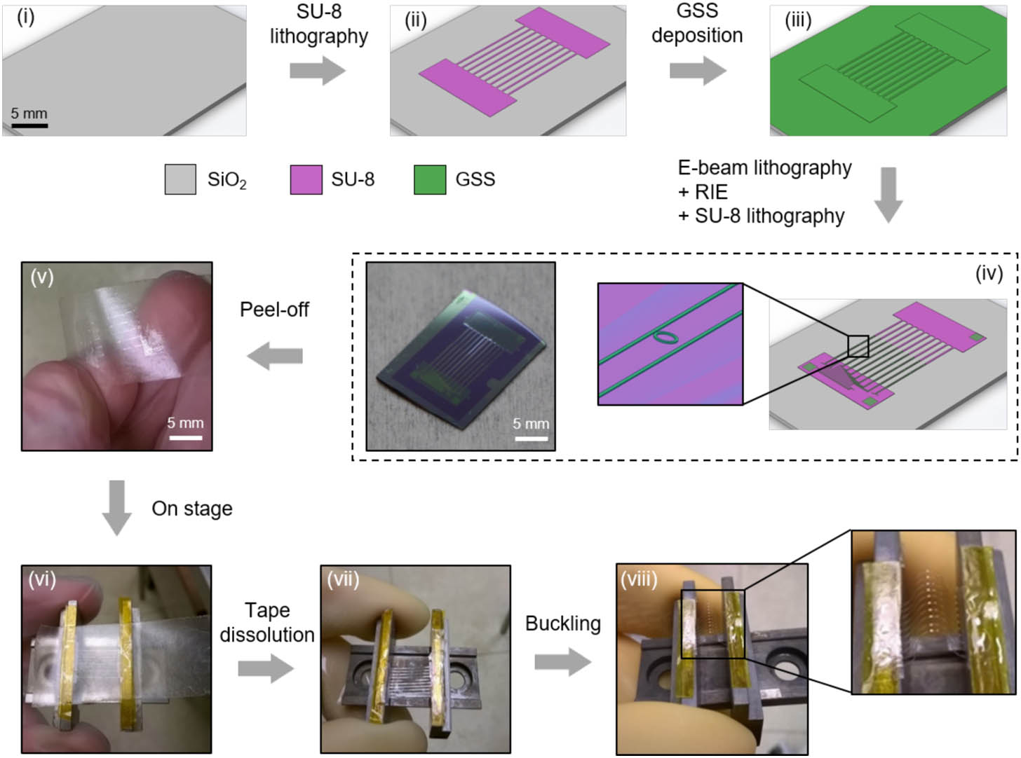
    Fig. 2. Overall fabrication process flow of the 3D integrated photonics devices.
    (a) Thickness map of the top cladding, showing the different thin/thick segments length ratios across the buckles. In practice, different thicknesses are realized by depositing a different number of cladding layers. (b) Picture of a corresponding sample fabricated using the mask. Two of the 10 buckles are missing after breaking during peel-off. (c) Comparison of the fabricated buckle shapes (full lines) with the theoretical predictions (dashed lines).
    Fig. 3. (a) Thickness map of the top cladding, showing the different thin/thick segments length ratios across the buckles. In practice, different thicknesses are realized by depositing a different number of cladding layers. (b) Picture of a corresponding sample fabricated using the mask. Two of the 10 buckles are missing after breaking during peel-off. (c) Comparison of the fabricated buckle shapes (full lines) with the theoretical predictions (dashed lines).
    (a) Buckled device with bonded 16-channel fiber array. On the left, a stress-relieving structure is used to increase the robustness of the packaged device. (b) Packaged device integrated in collagen. (c) Schematic integration process flow of the 3D sensor with a material of interest.
    Fig. 4. (a) Buckled device with bonded 16-channel fiber array. On the left, a stress-relieving structure is used to increase the robustness of the packaged device. (b) Packaged device integrated in collagen. (c) Schematic integration process flow of the 3D sensor with a material of interest.
    (a) 2D layout of the photonic device (purple) overlaid on top of the base SU-8 pattern (green). The temperature-tracking rings are boxed in red; the sensing rings are boxed in blue. (b) Resonant wavelength of the sensing resonator as a function of the peak of the temperature-tracking resonator, without any stress applied to the device. The error bars on the wavelength readings (both vertically and horizontally) are 1 pm (too small to be seen). Inset: transmission spectrum of a device over several free-spectral ranges (FSRs), with black (resp. red) arrows denoting temperature-tracking (resp. sensing) peaks, identified through the different FSRs of the two resonators. (c) Measured resonance shift as a function of local strain at the resonators. The linear fit equation is Δλ=3.2·Δϵ−0.04 nm. Inset: COMSOL model of the system, with a buckle being deformed by a moving block.
    Fig. 5. (a) 2D layout of the photonic device (purple) overlaid on top of the base SU-8 pattern (green). The temperature-tracking rings are boxed in red; the sensing rings are boxed in blue. (b) Resonant wavelength of the sensing resonator as a function of the peak of the temperature-tracking resonator, without any stress applied to the device. The error bars on the wavelength readings (both vertically and horizontally) are 1 pm (too small to be seen). Inset: transmission spectrum of a device over several free-spectral ranges (FSRs), with black (resp. red) arrows denoting temperature-tracking (resp. sensing) peaks, identified through the different FSRs of the two resonators. (c) Measured resonance shift as a function of local strain at the resonators. The linear fit equation is Δλ=3.2·Δϵ0.04  nm. Inset: COMSOL model of the system, with a buckle being deformed by a moving block.
    Schematic sideview of a uniform cross-section buckle.
    Fig. 6. Schematic sideview of a uniform cross-section buckle.
    Jérôme Michon, Sarah Geiger, Lan Li, Claudia Goncalves, Hongtao Lin, Kathleen Richardson, Xinqiao Jia, Juejun Hu. 3D integrated photonics platform with deterministic geometry control[J]. Photonics Research, 2020, 8(2): 194
    Download Citation