
Ying She, Chen Ji, Cheng Huang, Zuojun Zhang, Jianming Liao, Jiangyu Wang, Xiangang Luo, "Intelligent reconfigurable metasurface for self-adaptively electromagnetic functionality switching," Photonics Res. 10, 769 (2022)
- Photonics Research
- Vol. 10, Issue 3, 769 (2022)
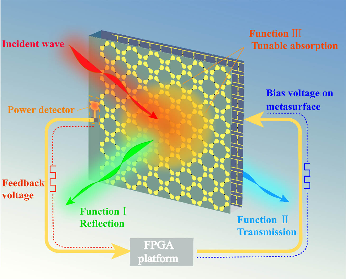
Fig. 1. Schematic configuration of the proposed intelligent metasurface.
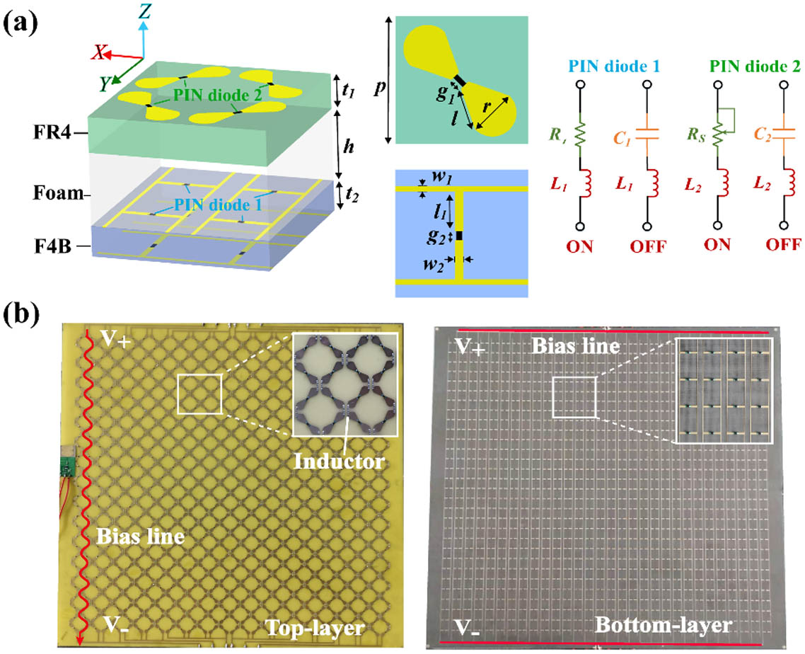
Fig. 2. (a) Geometrical model of the unit cell for the executing metasurface. (b) Photography of the fabricated metasurface sample. The metallic patterns on the top layer are serially connected in each row, while they are connected in parallel on the bottom layer.
Fig. 3. Simulated and measured reflection/transmission properties of the proposed executing metasurface under the different operation modes with the corresponding diode configurations of (PIN diode 1, PIN diode 2). (a) Reflection mode. (b) Transmission mode. (c), (d) Reflection and transmission properties at the tunable absorption mode.
Fig. 4. (a) Configuration of the sensing module for the incident power detecting. It is composed of an ultra-wideband patch antenna and a power detecting chip with the peripheral circuit. Values of the circuit parameters are chosen as follows: R 1 = 68 kΩ R 2 = 82 kΩ R 3 = 10 kΩ R 4 = 10 kΩ C 1 = 39 pF C 2 = 100 pF C 3 = 0.1 μF
Fig. 5. (a) Sketch of the measurement system for the intelligent metasurface and (b) photograph of the measurement setup in the microwave anechoic chamber.
Fig. 6. (a)–(g) Transmitted power intensity of the metasurface under the different incident power intensities at the frequency of 5, 5.2, 6, 7, 8, 9, and 10 GHz. (h), (i) Measured reflection and transmission of the proposed metasurface for the different illuminating power intensities.
|
Table 1. PIN Diode Configurations for the Different EM Functionalities of the Proposed Metasurface
|
Table 2. Mapping Relationship among the Incident Power Intensity, Received Feedback Voltage, and Controlling Bias Voltage for the Different Layers of the Proposed Metasurface


Set citation alerts for the article
Please enter your email address

© Copyright 2018-2021 | Chinese Laser Press. All Rights Reserved 沪ICP备15018463号-20