
Ying She, Chen Ji, Cheng Huang, Zuojun Zhang, Jianming Liao, Jiangyu Wang, Xiangang Luo, "Intelligent reconfigurable metasurface for self-adaptively electromagnetic functionality switching," Photonics Res. 10, 769 (2022)
- Photonics Research
- Vol. 10, Issue 3, 769 (2022)
Abstract
1. INTRODUCTION
During the past few decades, intelligent electromagnetic (EM) materials have attracted great attention owing to their tremendous application prospects, such as adaptive camouflage, intelligent cloaking, and smart skin [1]. Although there is no generally acknowledged definition of intelligent EM material, it can be understood as the ability to perceive external information and to make a feedback response with adaptive EM behavior to a changing environment [2]. A basic form of intelligent EM material can be defined on the material level by integrating various functional elements, including sensor, actuator, and memory [3]. Herein, the design of the material is very important, which is required to have the capability of handling multitasking for adapting their EM functionalities to the different environments. Recently, the emerging reconfigurable metasurface provides a good research platform for material design, because it can integrate various EM functionalities into itself, and these functionalities can be rapidly and dynamically switched with the external stimuli [4–8]. Therefore, the reconfigurable metasurface could be considered as a desirable candidate to construct intelligent EM material.
There have been various control mechanisms explored for the design of reconfigurable metasurface to achieve dynamic modulation of EM waves, such as thermal effect [9], electrical tuning [10], optical illumination [11], mechanical stretching [12], and micro-electro-mechanical systems (MEMS) [13]. Two typical structural forms have been developed to construct reconfigurable metasurfaces. One approach is to combine the passive metastructure with tunable materials, including phase change materials [14,15], two-dimensional (2D) materials (i.e., graphene and MoS2) [16–18], and liquid crystals [19], for realizing active function switching. The other one is to integrate positive–intrinsic–negative (PIN) diodes, or varactors into the design of metastructures, which is generally adopted by most of the existing reconfigurable metasurfaces at microwave frequencies [20–32]. One can dynamically control EM responses by tuning external bias voltages to the above lumped components. Many works have employed the PIN diodes to design 1-bit or multi-bit coding metasurfaces for wavefront manipulation [21–25]. In contrast to discrete phase modulation with PIN diodes, the continuous phase control can be realized by introducing varactors instead [26–28]. In addition, the PIN diode can be also used for constructing tunable absorbers by modulating its forward resistances [29,30]. Based on appropriate structure design with lumped components, reconfigurable metasurfaces can be established with multifunctional EM properties. In Ref. [31], a reconfigurable metasurface integrated with PIN diodes and varactors was proposed to simultaneously realize three different EM functionalities which are beam steering, polarization transformation, and backscattering reduction, respectively. In Ref. [32], the reported metasurface can be freely switched from transmission to reflection and then perfect absorption in real time. However, the abovementioned EM switching must rely on the control by human beings.
In order to achieve intelligent manipulation of EM waves without human intervention, reconfigurable metasurfaces should be further equipped with a sensor, actuator, and memory unit, which could rapidly and self-adaptively adjust its EM functionalities within the varying environment, just like a chameleon. Similar schemes have been proposed to design smart metasurfaces [33–35]. In the latest research [33], the smart metasurface integrated with a power detector was proposed to adaptively modulate the reflected patterns under the different microwave incidences. In Ref. [35], the intelligent cloak combining detectors and the deep-learning algorithm was reported, which can realize adaptive camouflage in response to the ever-changing incident wave and background through real-time phase compensation.
Sign up for Photonics Research TOC. Get the latest issue of Photonics Research delivered right to you!Sign up now
Here, an intelligent metasurface with the capability of self-adaptively EM manipulation is proposed. Compared with the traditional reconfigurable metasurface, it further integrates the sensing-and-feedback components to construct a closed-loop system without the aid of human beings. Our intelligent metasurface can first sense the incident EM power intensity, then acquire an operation instruction from the field programmable gate array (FPGA) controlling platform, and finally make dynamic switching of its EM functionality among reflection, transmission, and tunable absorption. Each of the EM functionalities depends on the power intensity of the incident EM wave. We have experimentally demonstrated that the proposed intelligent metasurface can not only realize high transmission for communication but also be switched to perform the strong absorption performance for reducing the probability of being detected by the threat radar. In addition, it can also behave the reflection property for avoiding EM interference. More importantly, the above EM functionalities are adaptively switched, which depends on the power intensity of the incident wave. Such design may inspire some potential applications in smart skin, radar radome, and the related EM fields.
2. DESIGN AND METHODS
A. Principle of the Intelligent Metasurface
Figure 1 shows the schematic configuration of the proposed intelligent metasurface, which consists of three main parts: power detecting module, FPGA controlling platform, and the executing material. The power detecting module serves as a sensor to perceive the intensity of the illuminating wave and then transforms the microwave signal into the feedback voltage for the FPGA controlling platform. The FPGA platform is mainly used for information processing, which can analyze the feedback voltage from the power detecting module and then send the proper instruction to the executing material for automatically adjusting its EM property with response to the changes of the EM environment. Many voltage configurations need to be pre-stored in the FPGA platform for controlling the operation state of the proposed executing material. Here, the executing material adopts the metasurface form that can generate three different EM functionalities including reflection, transmission, and tunable absorption by applying the corresponding voltage configuration to the loaded PIN diodes. When the power intensity of the incident EM wave is very low, the executing metasurface exhibits the high reflection property. If the power intensity is increased to a threshold value, it will be switched to the transmission function, which can realize communication with the outside. However, when the illuminating EM power intensity is continuously enhanced, the operation state of the proposed metasurface would be automatically changed to the absorption mode because the incoming wave may originate from threat radar in this case. In addition, the absorption performance would be gradually enhanced with the increase of the incidence intensity. All the above EM functionalities can be self-adaptively adjusted in the whole operation flow.
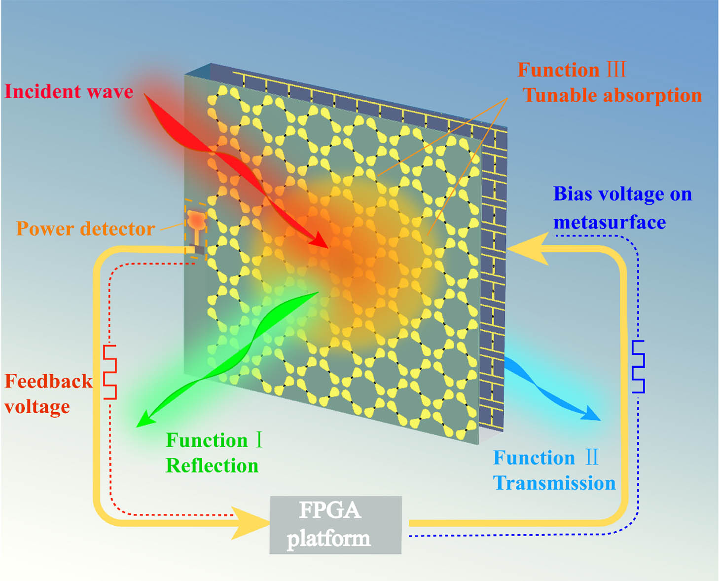
Figure 1.Schematic configuration of the proposed intelligent metasurface.
B. Design of the Reconfigured Metasurface
Figure 2(a) shows the geometrical model of the unit cell for the proposed executing metasurface, which is composed of two-layer functional structures separated by a foam spacer. The bottom-layer functional structure is made of two layers of T-type metallic patches, which are orthogonally arranged on both sides of a 0.508 mm thick F4B (
![]()
Figure 2.(a) Geometrical model of the unit cell for the executing metasurface. (b) Photography of the fabricated metasurface sample. The metallic patterns on the top layer are serially connected in each row, while they are connected in parallel on the bottom layer.
The geometrical parameters of the proposed metasurface are optimized as follows:
In order to demonstrate the tunable EM manipulation function of the proposed executing metasurface, the numerical simulation is conducted by the commercial software of CST Microwave Studio. The period boundary condition is set to the four sides of the unit cell for evaluating the infinite array. The Floquet port is defined as the exciting port to generate the plane wave normally incident onto the unit cell. Table 1 lists the operation states of the two kinds of PIN diodes corresponding to the three different EM functionalities of our metasurface. For the reflection mode, it is seen in Fig. 3(a) that high reflection property is obtained in the frequency range from 5 to 10 GHz when PIN diodes 1 and 2 respectively operate at the ON and OFF states. The measured average reflection loss is about 1 dB, indicating 79.4% reflectivity. If all the PIN diodes are switched off, the metasurface would be changed to the transmission mode where the insertion loss is less than 1.5 dB between 5 and 5.25 GHz as shown in Fig. 3(b). When PIN diodes 1 are switched on and the resistance of PIN diodes 2 is set as 80 Ω, it is obvious that there is almost no reflection and transmission at the frequency band of 4.8–10 GHz. As Figs. 3(c) and 3(d) show, both the reflection and transmission coefficients are lower than
PIN Diode Configurations for the Different EM Functionalities of the Proposed Metasurface
| Function | State of PIN Diode 1 | State of PIN Diode 2 |
|---|---|---|
| Reflection | ON | OFF |
| Transmission | OFF | OFF |
| Tunable absorption | ON | Tunable resistance |
| ON | ||
| ON |
![]()
Figure 3.Simulated and measured reflection/transmission properties of the proposed executing metasurface under the different operation modes with the corresponding diode configurations of (PIN diode 1, PIN diode 2). (a) Reflection mode. (b) Transmission mode. (c), (d) Reflection and transmission properties at the tunable absorption mode.
C. Design of the Sensing Module
To realize the self-adaptive response to the changes of environmental EM wave, the sensing module is designed as a power detector for perceiving the incident power intensity, which is directly integrated into the left side of the top-layer structure of the proposed executing metasurface. As Fig. 4(a) shows, the power detector is composed of an ultra-wideband (UWB) patch antenna and a power detecting chip (LTC5530 of Linear Technology) with its peripheral circuit. The UWB antenna is made of an elliptical-shaped patch and a defected ground, which can realize miniaturization and wideband impedance matching. It is seen in Fig. 4(b) that the antenna gain curve is relatively flat, and the gain varying range is lower than 1.5 dB at the frequency band of 5–10 GHz. In addition, the designed antenna keeps almost the same radiation patterns at different frequencies, which can effectively reduce the probability of power detecting error. The patch antenna perceives the incident EM wave power and then transmits it to an RF power detector of LTC5530 that can rectify the EM signals into the different feedback voltages. Figure 4(c) shows the measured feedback voltages corresponding to the different illuminating power intensities. When the illuminating power intensity varies from
![]()
Figure 4.(a) Configuration of the sensing module for the incident power detecting. It is composed of an ultra-wideband patch antenna and a power detecting chip with the peripheral circuit. Values of the circuit parameters are chosen as follows:
D. Design of the FPGA Controlling Platform
The FPGA controlling platform is designed for processing information and generating the proper instruction for the executing metasurface. It is mainly composed of an FPGA chip and analog-digital-analog (ADA) modules. The selected FPGA chip is XC6SLX9 from ALINX Electronics Technology, and each ADA module contains an analog-to-digital converter (ADC) submodule and a digital-to-analog converter (DAC) submodule. The AD conversion chip of the ADC submodule is AD7476 from Analog Devices, which can provide a digital output signal of 0–4095 corresponding to the input voltage of 0–12 V. Considering the received feedback voltage ranging from 0.83 to 5.7 V, the output digital signal of the ADC module would be located between 283 and 1946. The DAC submodule is equipped with a conversion chip of AD5621, which can provide the analog DC voltage of
Mapping Relationship among the Incident Power Intensity, Received Feedback Voltage, and Controlling Bias Voltage for the Different Layers of the Proposed Metasurface
| Function | Illuminating Power (dBm) | Feedback Voltage | Bias Voltage on Top-Layer Metasurface (V) | Bias Voltage on Bottom-Layer Metasurface (V) |
|---|---|---|---|---|
| Reflection | 0 | 1.5 | ||
| Transmission | −20 to −13 | 0.8–1 | 0 | 0 |
| Tunable absorption | −13 to −9 | 1–1.4 | 24–27 | 1.5 |
| −9 to −2 | 1.4–2.2 | 22–24 | 1.5 | |
| −2 to 10 | 19–22 | 1.5 |
3. EXPERIMENTAL MEASUREMENT AND DISCUSSION
To experimentally demonstrate the self-adaptive EM manipulation capability of the proposed intelligent metasurface, a measurement system as shown in Fig. 5 was set up in a microwave anechoic chamber. We utilized a vector network analyzer (VNA) and a power amplifier to generate an RF input signal with the adjustable power intensity for simulating the varying EM environment. The transmitted RF signal is captured by a spectrum analyzer through a low noise amplifier, while the reflected RF signal is received by another horn connected to the receiving port of the same VNA. With the variation of the illuminating power, our sample should automatically switch its EM functionalities.
![]()
Figure 5.(a) Sketch of the measurement system for the intelligent metasurface and (b) photograph of the measurement setup in the microwave anechoic chamber.
Figure 6 shows the transmitted power intensity and reflection of the metasurface under the different power illuminations. For the transmission measurement, the setup was normalized without a sample, and the illumination power at the position of the sample bracket is fixed as
![]()
Figure 6.(a)–(g) Transmitted power intensity of the metasurface under the different incident power intensities at the frequency of 5, 5.2, 6, 7, 8, 9, and 10 GHz. (h), (i) Measured reflection and transmission of the proposed metasurface for the different illuminating power intensities.
4. CONCLUSION
In summary, we have proposed an intelligent metasurface that can achieve self-adaptive EM manipulation with response to the different incident EM information. It is mainly composed of three parts: the sensing module, the FPGA controlling platform, and the executing material. The sensing module can perceive the power intensity of the incident EM wave, while the FPGA platform is used for information processing and thus sends the instruction to the executing material for switching its EM functionality among transmission, reflection, and tunable absorption. The whole metasurface establishes the complete sensing-feedback system, and its operation flow is automatic without human intervention. We have experimentally demonstrated the self-adaptive EM manipulation capability of our sample, which can make real-time and automatic adjustment of its operation state according to the perceived power intensity of the incoming wave. Compared with the traditional reconfigurable metasurface, our design further promotes the development of metasurfaces from manual control to self-adaptive control, which may find potential application in intelligent materials and systems.
5. EXPERIMENTAL SECTION
As shown in Fig. 5(b), the experimental setup was established in a microwave anechoic chamber. A VNA (R&S ZVA40) was adopted as the signal source and receiver for reflection measurement. Its port 1 was connected to a power amplifier with a gain of 20 dBi, and the amplified signal was transmitted through an LP standard horn (T-horn). The reflected signal was received by R-horn 1 connected to the other port of the VNA, while the transmitted signal would be captured by R-horn 2 and then transferred to the spectrum analyzer (R&S FSW50) through an LNA (with a gain of 15 dB). The distance between the T-horn (R-horn 1/2) and the sample is about 1.0 m. Here, the VNA was set as “CW mode,” which can achieve the signal output of a single frequency point. A DC power source (ITECH IT6322) was used to provide the constant offset voltage for the sample and FPGA platform. For the transmission measurement, the setup was normalized without a sample, and the illumination power is fixed as
References
[1] M. A. McEvoy, N. Correll. Materials that couple sensing, actuation, computation, and communication. Science, 347, 1261689(2015).
[2] C. Kaspar, B. Ravoo, W. van der Wiel, S. Wegner, W. Pernice. The rise of intelligent matter. Nature, 594, 345-355(2021).
[3] O. Tsilipakos, A. C. Tasolamprou, A. Pitilakis, F. Liu, X. Wang, M. S. Mirmoosa, D. C. Tzarouchis, S. Abadal, H. Taghvaee, C. Liaskos. Toward intelligent metasurfaces: the progress from globally tunable metasurfaces to software-defined metasurfaces with an embedded network of controllers. Adv. Opt. Mater., 8, 2000783(2020).
[4] T. Cui, B. Bai, H. Sun. Tunable metasurfaces based on active materials. Adv. Funct. Mater., 29, 1806692(2019).
[5] A. Nemati, W. Qian, M. Hong, J. Teng. Tunable and reconfigurable metasurfaces and metadevices. Opto-Electron. Adv., 1, 18000901(2019).
[6] C. Huang, J. Yang, X. Wu, J. Song, M. Pu, C. Wang, X. Luo. Reconfigurable metasurface cloak for dynamical electromagnetic illusions. ACS Photon., 5, 1718-1725(2017).
[7] C. Huang, B. Zhao, J. Song, C. Guan, X. Luo. Active transmission/absorption frequency selective surface with dynamical modulation of amplitude. IEEE Trans. Antennas Propag., 69, 3593-3598(2021).
[8] K. Chen, Y. Feng, F. Monticone, J. Zhao, B. Zhu, T. Jiang, L. Zhang, Y. Kim, X. Ding, S. Zhang. A reconfigurable active Huygens’ metalens. Adv. Mater., 29, 1606422(2017).
[9] M. Rahmani, L. Xu, A. E. Miroshnichenko, A. Komar, R. Camacho-Morales, H. Chen, Y. Zárate, S. Kruk, G. Zhang, D. N. Neshev. Reversible thermal tuning of all-dielectric metasurfaces. Adv. Funct. Mater., 27, 1700580(2017).
[10] A. de Lustrac, B. Ratni, G. P. Piau, Y. Duval, S. N. Burokur. Tri-state metasurface-based electromagnetic screen with switchable reflection, transmission, and absorption functionalities. ACS Appl. Electron. Mater., 3, 1184-1190(2021).
[11] M. R. Shcherbakov, S. Liu, V. V. Zubyuk, A. Vaskin, P. P. Vabishchevich, G. Keeler, T. Pertsch, T. V. Dolgova, I. Staude, I. Brener. Ultrafast all-optical tuning of direct-gap semiconductor metasurfaces. Nat. Commun., 8, 17(2017).
[12] H. S. Ee, R. Agarwal. Tunable metasurface and flat optical zoom lens on a stretchable substrate. Nano Lett., 16, 2818-2823(2016).
[13] E. Arbabi, A. Arbabi, S. M. Kamali, Y. Horie, M. S. Faraji-Dana, A. Faraon. MEMS-tunable dielectric metasurface lens. Nat. Commun., 9, 812(2018).
[14] S. H. Badri, M. M. Gilarlue, S. SaeidNahaei, J. S. Kim. Narrowband-to-broadband switchable and polarization-intensitive terahertz metasurface absorber enabled by phase change material. J. Opt., 24, 025101(2021).
[15] S. H. Badri, M. M. Gilarlue, S. G. Farkoush, S. B. Rhee. Reconfigurable bandpass optical filters based on subwavelength grating waveguides with Ge2Sb2Te5 cavity. J. Opt. Soc. Am. B, 38, 1283-1289(2021).
[16] C. Huang, J. Yang, C. Ji, L. Yuan, X. Luo. Graphene-driven metadevice for active microwave camouflage with high-efficiency transmission window. Small Methods, 5, 2000918(2021).
[17] H. Wang, C. Hao, H. Lin, Y. Wang, L. Lan, C. Qiu, H. Bao. Generation of super-resolved optical needle and multifocal array using graphene oxide metalenses. Opto-Electron. Adv., 4, 20003101(2021).
[18] B. Lee, J. Park, G. H. Han, H. Ee, C. Naylor, W. Liu, A. T. Charlie, J. Agarwal. Fano resonance and spectrally modified photoluminescence enhancement in monolayer MoS2 integrated with plasmonic nanoantenna array. Nano Lett., 15, 3646-3653(2015).
[19] R. Kowerdziej, M. Olifierczuk, J. Parka, J. Wrobel. Terahertz characterization of tunable metamaterial based on electrically controlled nematic liquid crystal. Appl. Phys. Lett., 105, 022908(2014).
[20] C. Huang, J. Song, C. Ji, J. Yang, X. Luo. Simultaneous control of absorbing frequency and amplitude using graphene capacitor and Active frequency-selective surface. IEEE Trans. Antennas Propag., 69, 1793-1798(2021).
[21] R. Wu, L. Bao, L. Wu, T. J. Cui. Broadband transmission-type 1-bit coding metasurfaces for electromagnetic beam forming and scanning. Sci. China Phys. Mech. Astron., 63, 284211(2020).
[22] T. J. Cui, M. Qi, X. Wan, J. Zhao, Q. Cheng. Coding metamaterials, digital metamaterials and programming metamaterials. Light Sci. Appl., 3, e218(2014).
[23] C. Huang, B. Sun, W. Pan, J. Cui, X. Wu, X. Luo. Dynamical beam manipulation based on 2-bit digitally-controlled coding metasurface. Sci. Rep., 7, 42302(2017).
[24] L. Zhang, Z. X. Wang, R. W. Shao, J. L. Shen, X. Q. Chen, X. Wan, Q. Cheng, T. J. Cui. Dynamically realizing arbitrary multi-bit programmable phases using a 2-bit time-domain coding metasurface. IEEE Trans. Antennas Propag., 68, 2984-2992(2020).
[25] Q. Ma, T. J. Cui. Information metamaterials: bridging the physical world and digital world. PhotoniX, 1, 1(2020).
[26] J. Liao, S. Guo, L. Yuan, C. Ji, C. Huang, X. Luo. Independent manipulation of reflection amplitude and phase by a single-layer reconfigurable metasurface. Adv. Opt. Mater., 2101551(2021).
[27] R. Feng, B. Ratni, J. Yi, H. Zhang, A. de Lustrac, S. N. Burokur. Versatile metasurface platform for electromagnetic wave tailoring. Photon. Res., 9, 1650-1659(2021).
[28] B. Liu, Y. He, S. W. Wong, Y. Li. Multifunctional vortex beam generation by a dynamic reflective metasurface. Adv. Opt. Mater., 9, 2001689(2021).
[29] H. L. Wang, H. F. Ma, M. Chen, S. Sun, T. J. Cui. A reconfigurable multifunctional metasurface for full-space controls of electromagnetic waves. Adv. Funct. Mater., 31, 2100275(2021).
[30] C. Huang, C. Ji, B. Zhao, J. Peng, L. Yuan, X. Luo. Multifunctional and tunable radar absorber based on graphene-integrated active metasurface. Adv. Mater. Technol., 6, 2001050(2021).
[31] C. Huang, C. Zhang, J. Yang, B. Sun, B. Zhao, X. Luo. Reconfigurable metasurface for multifunctional control of electromagnetic waves. Adv. Opt. Mater., 5, 1700485(2017).
[32] R. Phon, S. Ghosh, S. Lim. Novel multifunctional reconfigurable active frequency selective surface. IEEE Trans. Antennas Propag., 67, 1709-1718(2018).
[33] Q. Ma, G. D. Bai, H. B. Jing, C. Yang, L. Li, T. J. Cui. Smart metasurface with self-adaptively reprogrammable functions. Light Sci. Appl., 8, 98(2019).
[34] Q. Ma, Q. R. Hong, X. X. Gao, H. B. Jing, C. Liu, G. D. Bai, Q. Cheng, T. J. Cui. Smart metasurface with self-adaptively reprogrammable functions. Nanophotonics, 9, 3271-3278(2020).
[35] C. Qian, B. Zheng, Y. Shen, L. Jing, E. Li, L. Shen, H. Chen. Deep-learning-enabled self-adaptive microwave cloak without human intervention. Nat. Photonics, 14, 383-390(2020).
[36] H. Li, Q. Cao, L. Liu, Y. Wang. An improved multifunctional active frequency selective surface. IEEE Trans. Antennas Propag., 66, 1854-1862(2018).


Set citation alerts for the article
Please enter your email address

© Copyright 2018-2021 | Chinese Laser Press. All Rights Reserved 沪ICP备15018463号-20