
Mudassar Nazir, Xiaoyan Yang, Huanfang Tian, Pengtao Song, Zhan Wang, Zhongcheng Xiang, Xueyi Guo, Yirong Jin, Lixing You, Dongning Zheng. Investigation of dimensionality in superconducting NbN thin film samples with different thicknesses and NbTiN meander nanowire samples by measuring the upper critical field[J]. Chinese Physics B, 2020, 29(8):
- Chinese Physics B
- Vol. 29, Issue 8, (2020)
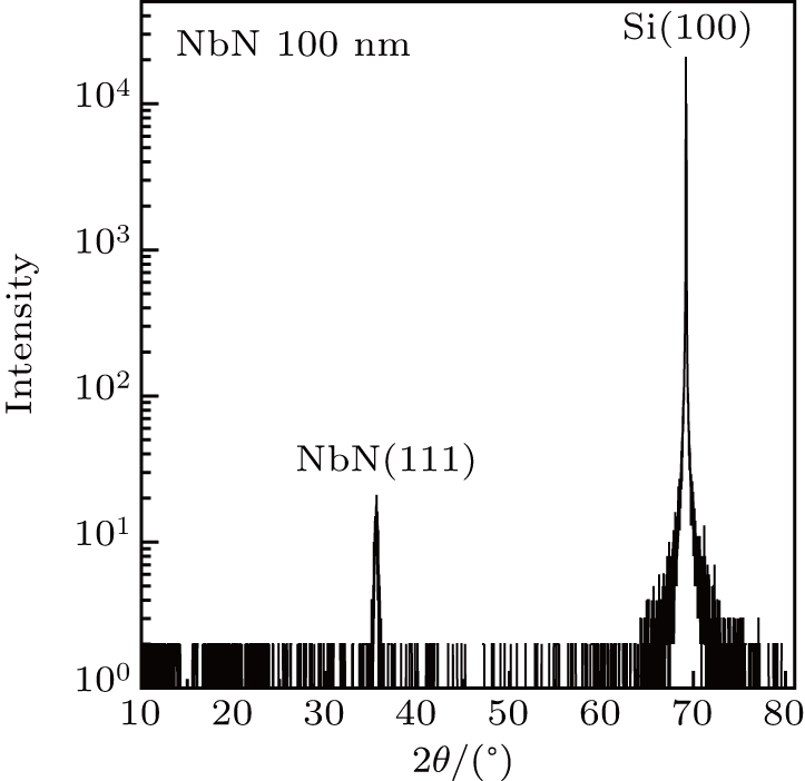
Fig. 1. XRD characterization of NbN 100 nm thin film.
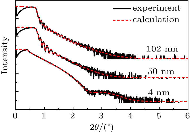
Fig. 2. XRR measurements were performed on NbN films of given thicknesses. Experimental results (black solid line) of the specimens were fitted (red short dash) by a multilayer model from bottom to top with the fitted NbN thicknesses shown.
Fig. 3. (a) Normalization of resistance as a function of temperature curves for different micro-bridges at zero fields. Inset: R –T is measured from 2 K to 300 K. (b) Thickness dependence of the transition temperature. The black solid symbols are experimental data and the red solid line is to guide the eyes.
Fig. 4. The R –T curves measured in different applied magnetic fields 0, 0.05, 0.1, 0.5, 1, 1.5, 2, 2.5, 3, 3.5, 4, 4.5, 5, 6, 7, 8, 9 (right to left, in units of T) for given specimens in both parallel and perpendicular orientations. By increasing the field, all curves move towards lower temperatures apparently and do not broaden.
Fig. 5. The temperature dependent parallel and perpendicular upper critical field diagrams. (a) The upper critical field for ultra thin 4 nm film and NbTiN 5 nm nanowire. The H c2∥(t ) shows pronounced 2D behavior and is well fitted with 2D GL Eq. (1 ) as indicated by the blue dash line. The black open circles and red open squares represent H c2∥(t ) for 4 nm NbN film and NbTiN 5 nm wire, respectively, and the H c2∥(t ) dependence shows a similar behavior. The solid triangles illustrate the H c2⊥(t ) data for NbN 4 nm film. (b), (c) The parallel critical field decreases while the perpendicular upper critical field rises with increasing thickness and the bending curvature moves towards T c. The H c2∥(t ) is explained with AGL interpolation crossover Eq. (2 ) and the perpendicular upper critical field data exhibit a linear behavior and are well fitted with Eq. (3 ). The arrows show t cr crossover temperature, and H c2(t ) shows crisscross in high thickness samples. The open circles and solid triangles represent parallel and perpendicular field experimental data, respectively, and are fitted using Eqs. (2 ) and (3 ) as shown by the red and green solid lines.
Fig. 6. Temperature dependence of the perpendicular upper critical field results for the ultra-thin NbN and the NbTiN nanowire samples. Bending curvature close to T c is observed and the red solid lines are the fitted curves using a (1−t )γ relation.
Fig. 7. Superconducting resistive transition curves under applied magnetic field 0 up to 9 T at different angles for (a) NbN 4 nm at temperature 7.8 K and (b) NbTiN 5 nm at 7.8 K. The upper critical field is defined at half of residual resistance and its angular dependence is shown for (c) NbN 4 nm and (d) NbTiN 5 nm nanowire. The sharp peak is seen at θ = 90° for given samples which is fitted with the 2D Tinkham and 3D anisotropic formulas given in Eqs. (4 ) and (5 ) as indicated by the red and blue solid lines, respectively. The black circles represent the experimental data. The inset shows a zoom-in view of the region around θ = 90°.
Fig. 8. (a) Angular dependence of upper critical field graph for NbN 100 nm is taken at temperature 11.25 K. The upper critical field shows maxima for both parallel and perpendicular orientations. The H c2 peak for the perpendicular orientation is believed to be due to the columnar structures formed during the growth of the thick films. (b) TEM image clearly shows columnar in NbN 100 nm film. The top, middle, and bottom layers represent the substrate, film, and protection layer, respectively. The red arrow indicates the one typical columnar structure.
Fig. 9. (a), (c) Angular variation of the resistance for NbN 4 nm thin and 100 nm thick films at fixed applied field for different temperatures. (b), (d) Polar plot of magneto-resistance is observed folding symmetry.
|
Table 1. The parameters, coherence lengths, and Tc defined at half of residual resistance for given samples.

Set citation alerts for the article
Please enter your email address
© Copyright 2018-2021 | Chinese Laser Press. All Rights Reserved 沪ICP备15018463号-20