• Opto-Electronic Advances
  • Vol. 5, Issue 8, 210119 (2022)
Pei Hang He1、2、†, Ling Yun Niu1、2、†, Yi Fan1、2, Hao Chi Zhang1、2、*, Le Peng Zhang1、2, Dayue Yao1、2, Wen Xuan Tang1、2, and Tie Jun Cui1、2、*
Author Affiliations
  • 1State Key Laboratory of Millimeter Waves, Southeast University, Nanjing 210096, China
  • 2Institute of Electromagnetic Space, Southeast University, Nanjing 210096, China
  • show less
    DOI: 10.29026/oea.2022.210119 Cite this Article
    Pei Hang He, Ling Yun Niu, Yi Fan, Hao Chi Zhang, Le Peng Zhang, Dayue Yao, Wen Xuan Tang, Tie Jun Cui. Active odd-mode-metachannel for single-conductor systems[J]. Opto-Electronic Advances, 2022, 5(8): 210119 Copy Citation Text show less
    The insulator-metal-insulator model.
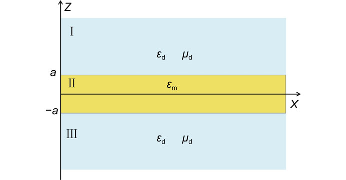
    Fig. 1. The insulator-metal-insulator model.
    Schematic diagram of the whole amplifier-integrated OMM.
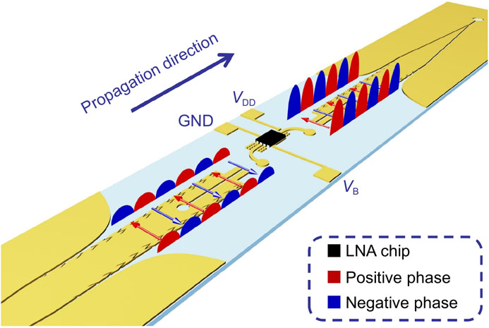
    Fig. 2. Schematic diagram of the whole amplifier-integrated OMM.
    Geometrical parameters and dispersion curves of the typical SSPP waveguide and the OMM. (a) Geometrical parameters of the typical SSPP structure, where the width of the center strip is w fixed as 4 mm, the period of the unit is p, the width of the grooves is a and the width of the narrow strip is w0. (b) Dispersion curves of the typical SSPP structure with varying a, where p = 1.5 mm, w0 = 1 mm. (c) Dispersion curves of the typical SSPP structure with varying p, where a = 0.75 mm and w0 = 1 mm. (d) Dispersion curves of the typical SSPP structure with varying w0, where p = 1.5 mm, a = 0.75 mm. (e) Geometrical parameters of the OMM, where the width of the center strip is w1 fixed as 4 mm, the period of the unit is p1, the width of the narrow strip is w01, the folding extent of the zigzag grooves is described by X and Y. (f) Dispersion curves of the typical SSPP structure with varying X, where w1 = 4 mm, w01 = 2.8 mm, a1 = 0.3 mm, p1 = 1.5 mm, Y = 0.2 mm.
    Fig. 3. Geometrical parameters and dispersion curves of the typical SSPP waveguide and the OMM. (a) Geometrical parameters of the typical SSPP structure, where the width of the center strip is w fixed as 4 mm, the period of the unit is p, the width of the grooves is a and the width of the narrow strip is w0. (b) Dispersion curves of the typical SSPP structure with varying a, where p = 1.5 mm, w0 = 1 mm. (c) Dispersion curves of the typical SSPP structure with varying p, where a = 0.75 mm and w0 = 1 mm. (d) Dispersion curves of the typical SSPP structure with varying w0, where p = 1.5 mm, a = 0.75 mm. (e) Geometrical parameters of the OMM, where the width of the center strip is w1 fixed as 4 mm, the period of the unit is p1, the width of the narrow strip is w01, the folding extent of the zigzag grooves is described by X and Y. (f) Dispersion curves of the typical SSPP structure with varying X, where w1 = 4 mm, w01 = 2.8 mm, a1 = 0.3 mm, p1 = 1.5 mm, Y = 0.2 mm.
    Cutoff frequency and decay factor curves with varying X, where the other parameters are the same with those in Fig. 3(f).
    Fig. 4. Cutoff frequency and decay factor curves with varying X, where the other parameters are the same with those in Fig. 3(f).
    Electric-field distributions of the cross sections of the SSPP structures at 15 GHz. (a–c) Absolute value of electric-field distributions on the cross-section of (a) even-mode of the typical SSPP (X = 0 mm) waveguide, (b) even mode and (c) odd mode of the OMM (X = 0.7 mm). (d) X-component, (e) Y-component and (f) Z-component of electric field of even mode of the OMM. (g) X-component, (h) Y-component and (i) Z-component of electric field of odd mode of the OMM. (j) X-component, (k) Y-component and (l) Z-component of electric field of slot line. (m) X-component, (n) Y-component and (o) Z-component of electric field of SOMM.
    Fig. 5. Electric-field distributions of the cross sections of the SSPP structures at 15 GHz. (ac) Absolute value of electric-field distributions on the cross-section of (a) even-mode of the typical SSPP (X = 0 mm) waveguide, (b) even mode and (c) odd mode of the OMM (X = 0.7 mm). (d) X-component, (e) Y-component and (f) Z-component of electric field of even mode of the OMM. (g) X-component, (h) Y-component and (i) Z-component of electric field of odd mode of the OMM. (j) X-component, (k) Y-component and (l) Z-component of electric field of slot line. (m) X-component, (n) Y-component and (o) Z-component of electric field of SOMM.
    The conversion structures. (a) Conversion structure between the quasi-TEM mode and odd-mode SSPPs, where 5 linearly gradient SSPP units are employed. (b) Simulated S-parameters of the conversion structure, where the OMM is composed of 46 units. (c) The compact conversion structure to convert odd-mode SSPP waves into voltage input of chips.
    Fig. 6. The conversion structures. (a) Conversion structure between the quasi-TEM mode and odd-mode SSPPs, where 5 linearly gradient SSPP units are employed. (b) Simulated S-parameters of the conversion structure, where the OMM is composed of 46 units. (c) The compact conversion structure to convert odd-mode SSPP waves into voltage input of chips.
    Experiments of the amplifier-integrated OMM. (a) Top view of the sample. (b) Bottom view of the sample. (c) Measured S-parameters of the sample. (d) The photograph of the EM scanning system composed of a VNA and a monopole probe installed in a mechanical platform in an EM shielding chamber. (e, f) The measured near-electric-field distributions of the amplifier-integrated OMM sample at (e) 14 and (f) 16 GHz.
    Fig. 7. Experiments of the amplifier-integrated OMM. (a) Top view of the sample. (b) Bottom view of the sample. (c) Measured S-parameters of the sample. (d) The photograph of the EM scanning system composed of a VNA and a monopole probe installed in a mechanical platform in an EM shielding chamber. (e, f) The measured near-electric-field distributions of the amplifier-integrated OMM sample at (e) 14 and (f) 16 GHz.
    Crosstalk suppression and low RCS properties of the OMM. (a) Coupling pair of SSPP channel. (b) Crosstalk of typical even-even coupling pair and odd-even coupling pair. (c) RCS of the OMM compared to that of a CPW with the same total size.
    Fig. 8. Crosstalk suppression and low RCS properties of the OMM. (a) Coupling pair of SSPP channel. (b) Crosstalk of typical even-even coupling pair and odd-even coupling pair. (c) RCS of the OMM compared to that of a CPW with the same total size.
    Flexibility test of the amplifier-integrated OMM.
    Fig. 9. Flexibility test of the amplifier-integrated OMM.
    Radius13 GHz14 GHz15 GHz16 GHz17 GHz
    11 cm3.516.213.16.316.8
    14 cm3.415.813.77.316.7
    22 cm6.022.317.514.918.9
    Table 0. Flexibility test of gain (dB) of the amplifier-integrated OMM.
    ParametersValues (mm)ParametersValuesParametersValues (mm)ParametersValues (mm)
    r10.9Lt20 mmr30.6r40.7
    r20.9Lx12.5 mmSs0.3r50.7
    d11Ly6 mmLs18.85d30.9
    d21.2ac0.00587Ls22.1d40.7
    S0.2bc2Ls33.1Wg9.4
    Wm0.4cc0.8Ws0.7
    i0.6g0.2 mmLg14.3
    Table 0. Geometrical parameters of the conversion structures.
    ParametersExEyEz
    Even mode of the OMM18.50730.00121
    Odd mode of the OMM0.527325.87231
    Odd mode of the SOMM2.99593.1391
    Mode of the slot line0.1611.65561
    Table 0. Normalized field integral of different modes.
    Pei Hang He, Ling Yun Niu, Yi Fan, Hao Chi Zhang, Le Peng Zhang, Dayue Yao, Wen Xuan Tang, Tie Jun Cui. Active odd-mode-metachannel for single-conductor systems[J]. Opto-Electronic Advances, 2022, 5(8): 210119
    Download Citation