Andrey S. Sokolov1, Haider Abbas1, Yawar Abbas2, and Changhwan Choi1
Abstract
Resistive random-access memory (RRAM), also known as memristors, having a very simple device structure with two terminals, fulfill almost all of the fundamental requirements of volatile memory, nonvolatile memory, and neuromorphic characteristics. Its memory and neuromorphic behaviors are currently being explored in relation to a range of materials, such as biological materials, perovskites, 2D materials, and transition metal oxides. In this review, we discuss the different electrical behaviors exhibited by RRAM devices based on these materials by briefly explaining their corresponding switching mechanisms. We then discuss emergent memory technologies using memristors, together with its potential neuromorphic applications, by elucidating the different material engineering techniques used during device fabrication to improve the memory and neuromorphic performance of devices, in areas such as ION/IOFF ratio, endurance, spike time-dependent plasticity (STDP), and paired-pulse facilitation (PPF), among others. The emulation of essential biological synaptic functions realized in various switching materials, including inorganic metal oxides and new organic materials, as well as diverse device structures such as single-layer and multilayer hetero-structured devices, and crossbar arrays, is analyzed in detail. Finally, we discuss current challenges and future prospects for the development of inorganic and new materials-based memristors.1. Introduction
With the increase in demand for memory storage technology, the physical limitations of conventional silicon (Si)-based memory devices represent a major challenge for further miniaturization[1, 2]. With a comparatively high voltage and low retention time, flash memory is currently the most dominant memory technology on the market[3, 4]. However, it has almost reached its physical and technological limits; as a result, meeting the requirements of future or next-generation memory technology represents a major challenge[5, 6]. Due to these limitations, interest in the development of new and next-generation memory technology has increased in both industry and academia[7-9].
Depending on the data storage time, memory is classified as either volatile memory or nonvolatile memory[10-12]. In volatile memory devices, information can be stored for a short time (i.e., temporarily). In contrast, data can be stored in nonvolatile memory devices for a long time (i.e., permanently), typically for a period of years[5]. The information in memory devices can be stored in the form of charge[13, 14], the alignment of magnetic domains[15, 16], phase[17, 18], and resistance state in the material[19-21]. Researchers have struggled to adapt various engineering techniques in order to achieve improvements in these memory technologies in terms of retention, endurance, memory density, and low power consumption. Proposed memory technologies include ferroelectric random-access memory (FeRAM)[22], magnetic random access memory (MRAM)[23], phase-change random access memory (PCRAM)[24], and resistive random access memory (RRAM)[25-27].
With sub-nanosecond switching speed[28, 29], very high endurance[30, 7] and low power consumption capability[31, 32], RRAM is considered to be the ideal replacement for nonvolatile memory in the future, and it is anticipated to revolutionize the future of memory technology in every respect. RRAM is a two-terminal memory device with a stacked structure of metal–insulator–metal (MIM)[33], where the metals are considered as top electrode (TE) and bottom electrode (BE) and the insulator is referred to as the switching medium. Since the information stored in RRAM is contained in the resistance state of the device, RRAM is also known as a memristor (a portmanteau word, comprising ‘memory’ and ‘resistor’)[34, 35]. The resistance of RRAM can be altered via the appropriate application of a voltage sweep or pulse. The process of changing a device’s resistance from a high resistance state (HRS) to a low resistance state (LRS) is known as the SET process. Conversely, when a device’s resistance switches from LRS to HRS, the process is referred to as the RESET process. In general, RRAM devices are found to be in HRS in their pristine state[36, 37]; however, depending on the fabrication conditions, a device could potentially be in LRS in its pristine state[38, 29]. The acknowledged benchmark mechanism for resistance change in RRAM devices among the RRAM community is either via the migration of oxygen vacancies[39-41] or the migration of active metal ions (Ag or Cu)[42, 30, 29]. The RRAM variants based on resistance changes due to the migration of vacancies are known as valence change random access memory (VCRAM)[43], and those based on resistance change caused by the migration of metal ions are referred to as conductive bridge random access memory (CBRAM)[44] or electrochemical metallization memory (ECM) cells[45, 46]. The memory characteristics exhibited by RRAM depend on the selection of appropriate TE, BE and switching media[20, 47, 48], whose characteristics can be improved by different engineering techniques, which we will discuss in detail in the later sections of this review.
Moreover, as with the technical and scaling limitations faced by conventional memory devices, conventional computing systems also face challenges in terms of computing efficiency and computing capacity. The conventional computing system is based on the well-known von Neumann computing architecture. The separation between the memory and processing units in a von Neumann architecture, the so-called von Neumann bottleneck, limits the efficiency of current computing systems. Therefore, neuromorphic computing, with its in-memory-computing capabilities, may prove useful in the development of a new computing paradigm, overcoming the von Neumann bottleneck. For the realization of a neuromorphic computing system, the emulation of essential biological functions is a key step[49]. Of the various emerging technologies investigated in relation to the emulation of biological synaptic functions, the memristor is a promising candidate, owing to its simple two-terminal structure, low power consumption, and fast switching speed.
In this review, we discuss various materials-based RRAM devices for non-volatile memory applications, as well as for emerging neuromorphic applications. In Section 2, we focus on different materials used as switching media in memristive devices and their electrical characteristics, as reported in the literature, explaining the mechanism for these electrical behaviors with a brief summary of the general biology underpinning the electronic synapse. Section 3 presents recent applications of memristors in memory technology. This section discusses the different switching materials and engineering methodologies used to improve non-volatile memory characteristics, such as ION/IOFF ratio, retention, switching speed and endurance. Section 4 discusses the application of memristors for neuromorphic engineering using different materials, and their respective engineering techniques. Finally, Section 5 elaborates on future directions for memory technology and neuromorphic engineering using memristors.
2. Fundamentals of memristors and neuromorphic computing
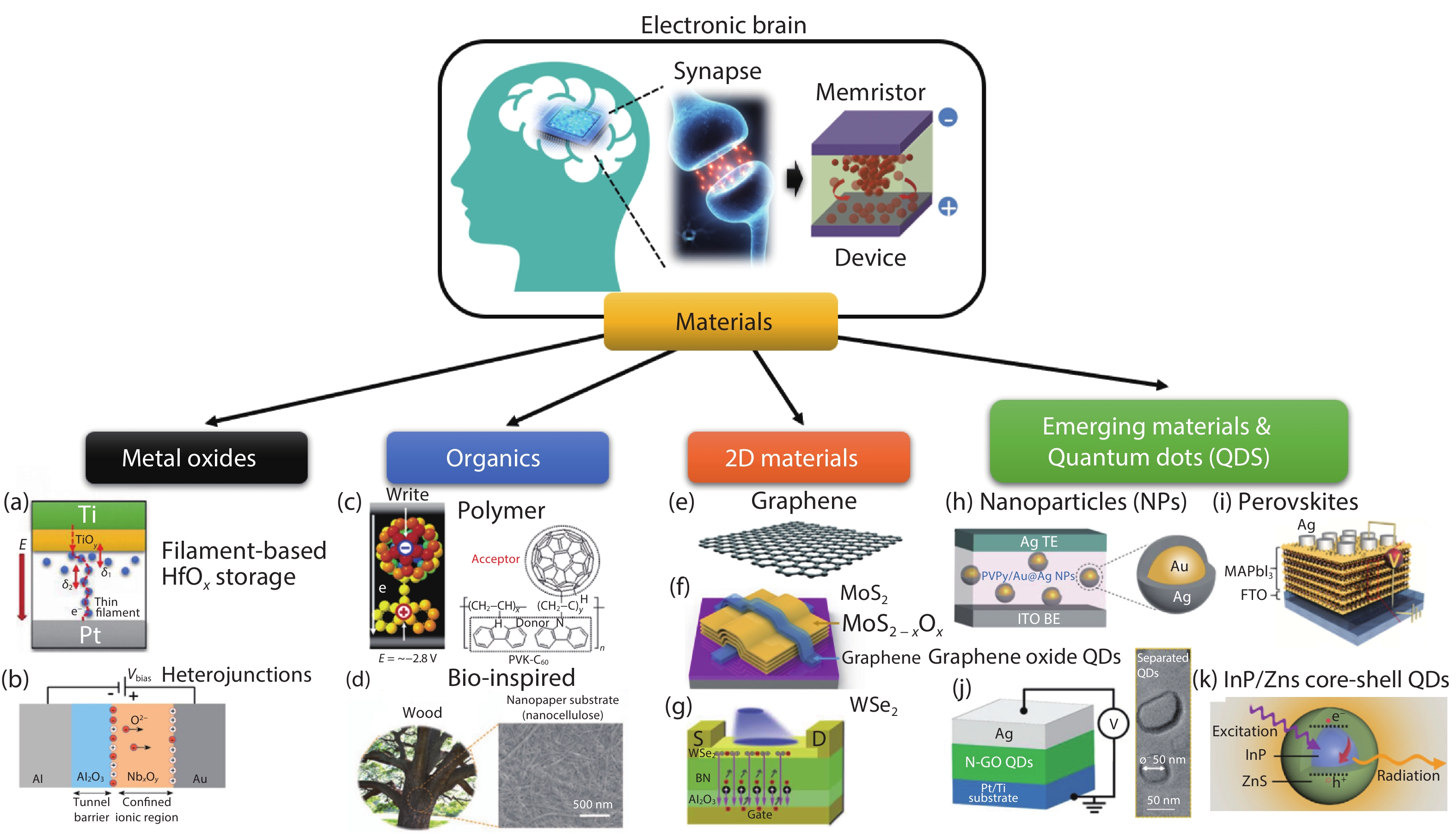
Emerging memristor technology possesses a variety of advantages, such as non-volatility, simple structure, nanometer cell size, and, importantly, low-power operation. Therefore, the investigation of new materials possessing resistive switching characteristics, is key to the realization of upgraded memristor devices, which can also be utilized as artificial synapses, as illustrated in Fig. 1. This artificial synapse technology is in high demand for hardware-based neuromorphic computing, given the rapid growth of software analog applications such as sensors, the internet of things (IoT), robotics, and artificial intelligence (AI)[50]. Compared with classic von Neumann computing, neuromorphic computing operates in a largely parallel fashion, with a high operating speed, consuming little energy, and with minimal size-volume requirements. Therefore, artificial synapses, being a basic building block of neuromorphic computing, are required to be explored in relation to any material broadly capable of emulating the crucial functions of the brain. Memristor operation as a single synapse unit is of great value, due to the absence of a peripheral circuit; memristor-based crossbar architecture can therefore operate in a highly parallel fashion, at high speed[51]. To date, various materials displaying memristive properties have been explored, as shown in Fig. 1. These comprise simple transition metal oxides (TMO)[52, 41, 53, 54], structured inorganic oxides[55, 56, 42], perovskites[32, 57], polymers[58, 59], 2D materials[60-64], organic materials[65, 66], and low-dimensional emerging materials[67]. While each material facilitates resistive switching (RS) in memristors, artificial synapse characteristics differ greatly depending on the type of material employed, which result in enhanced performance in both memristors and synapse devices, respectively. The materials mentioned above are primarily discussed in this review from the perspective of emerging memristor memory devices, followed by neuromorphic memristor-based artificial synapse devices. Recent reviews have focused on switching materials for memristors, examining resistive switching filament controls for synapse applications[68] and different types of memristor materials[69], as well as collating studies relating to the thickness, doping and specific design of memristor devices[70].
![(Color online) Recent materials used for memristive storage and applied in artificial synapses. (a) The sketch of filamentary-based resistive switching in an inorganic metal oxide (HfOx) memristor. Reprinted from Ref. [41]. (b) Schematic of inorganic metal oxide-based hetero-structured device, as Al/Al2O3/NbxOy/Au device. Reprinted from Ref. [52]. (c) Chemical diagram and schematic of polymer-based PVK-C60 memristive device. Reprinted from Ref. [58]. (d) Naturally extracted nanocellulose-based memristive device. Reprinted from Ref. [65]. (e) 2-dimensional (2D) shape of graphene. Reprinted from Ref. [71]. (f) 2D material MoS2, sandwiched between graphene electrode-based memristive device. Reprinted from Ref. [61]. (g) 3-terminal memristive device based on WSe2 2D material. Reprinted from Ref. [64]. (h) Schematic of PVPy-doped Au@Ag bimetal nanoparticle memristor storage. Reprinted from Ref [72]. (i) Sketch of an Ag/MAPbI3/FTO organic-inorganic hybrid perovskite artificial synapse device. Reprinted from Ref. [32], (j) Graphene oxide (GO) quantum dots (QDs) -based memristive storage device. Reprinted from Ref. [73], (k) InP/ZnS core-shell QDs-based memristive device, applied as an artificial synapse. Reprinted from Ref. [74].](/Images/icon/loading.gif)
Figure 1.(Color online) Recent materials used for memristive storage and applied in artificial synapses. (a) The sketch of filamentary-based resistive switching in an inorganic metal oxide (HfOx) memristor. Reprinted from Ref. [41]. (b) Schematic of inorganic metal oxide-based hetero-structured device, as Al/Al2O3/NbxOy/Au device. Reprinted from Ref. [52]. (c) Chemical diagram and schematic of polymer-based PVK-C60 memristive device. Reprinted from Ref. [58]. (d) Naturally extracted nanocellulose-based memristive device. Reprinted from Ref. [65]. (e) 2-dimensional (2D) shape of graphene. Reprinted from Ref. [71]. (f) 2D material MoS2, sandwiched between graphene electrode-based memristive device. Reprinted from Ref. [61]. (g) 3-terminal memristive device based on WSe2 2D material. Reprinted from Ref. [64]. (h) Schematic of PVPy-doped Au@Ag bimetal nanoparticle memristor storage. Reprinted from Ref [72]. (i) Sketch of an Ag/MAPbI3/FTO organic-inorganic hybrid perovskite artificial synapse device. Reprinted from Ref. [32], (j) Graphene oxide (GO) quantum dots (QDs) -based memristive storage device. Reprinted from Ref. [73], (k) InP/ZnS core-shell QDs-based memristive device, applied as an artificial synapse. Reprinted from Ref. [74].
In addition, we focus on the different electrical characteristics reported in relation to memristors. Depending on the fabrication method, structural stacking, and conditions of the electrical measurements (such as stopping voltage and compliance current), a memristor exhibits different (current–voltage) I–V characteristics. There is general agreement in the memristor community regarding the key electrical characteristics exhibited by memristors. Although most published research is based on capacitor structure, the main goal is to achieve a transistor-less crossbar array with a 100% device yield[75] to fulfill the market requirements. Fig. 2 shows a schematic diagram of a memristor, with the different electrical characteristics exhibited by RRAM, given in the literature. Fig. 2(a)[76] shows an atomic force microscope image of a crossbar array, and the inset shows the schematics of an MIM at the cross point. Fig. 2(b)[73] shows the schematics of a synapse, considered to be the biological analog of the memristor. Figs. 2(c)[77] and 2(d)[78] show the digital and abrupt switching characteristics of RRAM, respectively referred to as bipolar resistive switching (BRS) and unipolar resistive switching (URS. In BRS (Fig. 2(c)), the filament is formed for one polarity of applied bias with appropriate compliance current, whereas the filament breaks or dissolves for the opposite polarity. In the case of URS, filament formation and breakdown take place for the same polarity of applied voltage, as shown in Fig. 2(d). The independence of filament breakdown on the voltage polarity is evidence that the switching from LRS to HRS in URS is caused by the joule heating effect[79, 80]. It should be noted that BRS and URS characteristics are observed both in VCRAM[81, 82] and CBRAM[29, 80]. Multilevel resistive switching is also achieved in a single device by controlling the compliance current during the SET process, as shown in Fig. 2(e)[83]. Multilevel switching is favorable for improving a device’s memory density[84]. Unlike abrupt resistance change switching characteristics, Fig. 2(f)[75] depicts gradual switching characteristics. Gradual switching is also a type of digital switching, but one cannot observe an abrupt change in resistance at specific voltages (i.e., SET and RESET voltages). Recently, gradual switching has been observed in an Si-based memristor crossbar array with alloyed conduction channels[75]. Similar switching can be obtained by permitting moments of vacancy at the interface of the metal electrode and the oxide[85]; as a result, this type of switching is referred to as interface switching[86, 87].
Figure 2.(Color online) Memristor and resistive switching characteristics. (a) Atomic force micrograph of 17 × 17 nano-cross bar array: the inset shows the schematic structure of the cross point. Reprinted from Ref. [76]. (b) Representation of biological synapse, including pre-/postsynaptic neurons and synaptic cleft. Reprinted from Ref. [73]. (c) Bipolar resistive switching characteristic with insets depicting the electroforming process and scanning electron microscope image of a 100 × 100 μm2 device. Reprinted from Ref. [77]. (d) Unipolar resistive switching characteristics. (e) Multi-level resistance states at different compliance currents. Reprinted from Ref. [78]. (f) The gradual switching performance of a Si memristor with an Ag–Ti alloy. Reprinted from Ref. [75]. (g) The complementary resistive switching behavior achieved by tailoring nanoplateau structures using solution-processed rutile TiO2 thin films. Reprinted from Ref. [30]. (h) Analog resistive characteristic induced by the structural engineering of a tantalum oxide-based memristor. Reprinted from Ref. [56]. (i) The threshold resistive switching I–V characteristics of N-GOQDs-based devices. The inset shows the controlled repetitive threshold switching I–V characteristics of the device under an Icc of 50 µA. Reprinted from Ref. [73]
Because of the gradual change in resistance (absence of abruptness) during the application of a single sweep, gradual switching or interfacial switching provides a perfect platform for the application of memristors in artificial neuromorphic systems. The transistor-less architecture of the crossbar array is extremely appealing with regard to high memory density[75, 88, 49]. However, the sneak current through the cross point of the crossbar, particularly when the cells are in LRS, causes higher power consumption and errors in reading operations. Fig. 2(g)[30] illustrates complementary resistive switching (CRS)[89, 90], which is proposed as the most appropriate switching to eliminate excess power consumption due to sneak path currents in crossbar arrays. Fig. 2(h)[56] shows the analog resistive switching characteristics of an oxide-based memristor. In these devices, conductance increases with the application of consecutive positive sweeps, and conductance decreases over successive negative sweeps[91, 92]. The change in conductance is ascribed to the re-distribution of oxygen vacancies[93, 54]. Such characteristics are also achieved in layered structures with Ag-rich and Ag-poor regions via the appropriate design of the Ag/Si mixture ratio gradient. Here, conductance can be controlled via the moment of Ag+ between the regions[94]. Finally, Fig. 2(i)[73] depicts threshold resistive switching characteristics[95, 96]. The resistance of the device decreases when an external bias is applied to the top electrode by the formation of Ag or Cu-based channels. Nevertheless, unlike CBRAM, the resistance recovers spontaneously when the applied electric field is removed. Threshold switching devices are also known as ‘diffusive memristors’[97], and threshold switching offers unique temporal conductance evolution dynamics, making it suitable for innovative applications in both systems and circuits[98, 99]. In addition, the self-dissolution of the filament in diffusive memristors is caused by the minimization of interfacial energy[100-102].
As mentioned in the introduction, current computing systems are largely based on a von Neumann architecture. For a general-purpose computer, this architecture works well, and is useful and convenient for performing simple tasks. However, these conventional computing systems are inefficient in relation to the data-intensive tasks associated with a big data era. The separation between processing and memory units is a bottleneck for data transfer, limiting efficiency. In recent years, neuromorphic computing has emerged as a promising computing technology, offering an alternative to the von Neumann architecture. The neuromorphic computing system combines memory and processing into a single unit, similarly to the biological brain. The human brain has ~1011 neurons, which act as the main processing unit. These neurons are connected by ~1015 reconfigurable connections called synapses, which are responsible for learning and memory[103]. For the implementation of a neuromorphic system in hardware terms, it is essential to realize an effective emulation of biological synaptic function using artificial synapses. Of the various devices investigated in the context of artificial synapses, the memristor, being a two-terminal device, most closely resembles the biological synapse, exhibiting several promising synaptic characteristics, as shown in Fig. 3. Synapses play a key role in the performance of learning and memory functions in the brain. The strength of the connection between two neurons lies in the weight of the synapse connecting them. Synaptic weight changes in a sequential manner during the learning process[104]. Therefore, the memristor synapse must also exhibit such a weight modulation (conductance) in an analog fashion, in order to effectively mimic synaptic plasticity. Figs. 3(a) and 3(c) correlate the potentiation and depression characteristics of a biological synapse and an electronic memristor synapse, respectively[105, 106]. Moreover, to demonstrate the feasibility of an electronic device for neuromorphic computing applications, it is essential that the device demonstrates Hebbian learning rules, such as spike-timing-dependent plasticity (STDP). The STDP behavior of the biological synapse is depicted in Fig. 3(b)[105]. The emulation of STDP behavior by a memristor synapse is shown in Fig. 3(d)[106]. The STDP behavior emulated by the artificial synapse demonstrates a good correlation with that of the biological synapse, which confirms the feasibility of the memristor synapse for neuromorphic computing applications.
Figure 3.(Color online) Memristor synapse mimicking the representative synaptic functions of biological synapses for neuromorphic computing applications. (a) Synaptic potentiation and depression behavior of biological synapses obtained from a pair of glutamatergic neurons in hippocampal culture. (b) STDP behavior of biological synapse. Reprinted from Ref. [105]. (c) LTP/LTD characteristics exhibited by a memristor synapse. (d) STDP behavior, mimicked by a memristor-based artificial synapse, which follows the asymmetric Hebbian learning rule. Reprinted from Ref. [106].
3. Emergent memory technology with memristors
In this section, we discuss emerging memory technology using memristors, their resistive switching (RS) properties and characteristics, and common engineering techniques for achieving the desired memory RS behavior for applied memory storage. Section 3.1 describes ternary oxides, such as ABOx-based memristors, focusing on ternary oxides the superior RS characteristics of ternary oxides as compared to simple binary oxides, due to the extended defect chemistry considerations of ternary oxides. Section 3.2 further explains doping effects on binary transition metal oxides (TMO) and their evident modulation of RS behavior for the achievement of desired characteristics. Primarily, this discussion focuses on methods of dopant engineering and specific dopant implantation, respectively. Section 3.3 discusses memory advances in bi-layered memristors, together with their respective RS characteristics. Specifically, we examine the RS improvement in memristors, due to the redistribution of switching ions in the filament, and the potential for controlling volatile/non-volatile properties, including multi-level RS behaviors. Section 3.4 further discusses the influence of oxide stack sequences on RS behaviors in memristor devices. Briefly, by stacking sequence of oxides, the RS behavior of a memristor can be substantially tuned, for example, from bipolar RS to unipolar RS; however, control of the stoichiometry of bi-layered oxides is key, since oxide stoichiometry affects the migration movement of ions.
3.1. Memory advances with ternary memristors
Ternary metal oxides (TMOs), also known as ABOx structures, exhibit superior electrochemical performance as compared to binary oxides. Specifically, TMOs can retain multiple oxidation states and, therefore, demonstrate superior resistive switching memory characteristics, such as reduced randomness in switching filament formation, stabilization of SET/RESET voltage values, and an improvement in overall uniformity[107, 108]. Research into memristors has been widely conducted, employing a variety of TMOs as a switching media. For example, Faita et al. studied oxygen-rich / oxygen-poor, as well as bilayer structured HfAlOx based memristors, demonstrating improved multilayer resistive switching characteristics[108]. Wang et al. researched ZnAl2O4 thin films for memristor applications, discovering unipolar resistive switching with a resistance ratio of one order, impressive endurance, and long retention time[109]. Katiyar et al. investigated a unipolar resistive switching with a polycrystalline BiFeO3-based planar memristor, reporting non-overlapping SET/RESET voltages, high resistance ratio of ~104, and a long memory state retention of ~3000 s[110]. Non-volatile resistive switching has also been observed in LaAlO3/SrTiO3 heterostructures, in which switching is attributed to the reversible transition between tunneling and Ohmic characteristics, possibly due to the charged movement of oxygen vacancies via the LaAlO3/SrTiO3 interface, as observed by Wu et al.[111] Detailed studies of the origin and mechanisms of nanofilament formation, responsible for memory resistive switching, in polycrystalline ternary SrTiO3 based memristors, have been conducted by Kwon et al., highlighting the SrTi11O20 conducting phase identified at specific grain boundaries, which is driven by electrochemical polarization and nearby oxygen activity[112]. Modulated resistive switching, functioning as both non-homogeneous and homogeneous memory, has been observed by Hu et al., who note that by changing the crystal structure of LiCoO2 based memory storage from the amorphous to the R-3m crystal phase, different fingerprints of resistive switching can be obtained[113]. To conclude, the ternary phase ABOx-type oxides, from conventional varieties such as HfAlOx, HfZrOx, etc., to unconventional types such as LiCoO2 etc., with their intriguing physical and chemical properties in terms of broad defect chemistry variations, represent the next stage of research into next-generation memory devices, capable of stable operation, based on the resistive switching (RS) phenomenon.
Advances in memory technology based on ternary ABOx oxide storage have tremendous potential, due to combined memory attributes, such as resistive switching, ferroelectricity, ferromagnetism, and photovoltaic effects[114]. The superiority of ternary oxides over binary oxides inemerging memory storage matrices has been demonstrated by means of recent advances in resistive memory. Sokolov et al. researched three ALD-based types of memory storage oxides, Al2O3, HfO2, and HfAlOx, in the same device structure as that shown in the TEM image in Fig. 4(a). Superior resistive switching behavior was found in the HfAlOx based memristor in comparison to simple binary oxides in terms of higher resistance ratio (> 102), more uniform SET/RESET voltages, and longer endurance and retention[53]. The authors concluded that a highly thermally stable amorphous phase in the HfAlOx thin film allows for more controllable switching filament formation, resulting in the improved self-compliance resistive switching behavior of the HfAlOx based memristor, as against binary Al2O3 and HfO2-based memristors, as shown in Fig. 4(b). Effective oxygen scavenging from HfAlOx oxide by the reactive Ti top electrode, along with defect chemistry considerations of intermixing Al2O3 and HfO2 oxides, where Al interstitials of Hf sites also give out additional oxygen vacancies, is responsible for this effective switching filament formation, generated by oxygen vacancies, as displayed in Fig. 4(c). Resistive switching associated with ferroelectric polarization has been researched in relation to ternary Hf0.5Zr0.5O2 epitaxial thin films by Sulzbach et al., as shown in Fig. 4(d)[115]. Capping dielectrics, such as crystalline SrTiO3 and amorphous AlOx, can block unnecessary ionic drift via grain boundaries of m-HZO and o-HZO, allowing for better homogenic polarization, and improving the overall performance of resistive switching memory devices, as depicted in Fig. 4(e). Strained interface heterostructures with ternary ABOx based memristive devices could represent a further possible approach to the construction of resistive switching memory devices. Designed by Schweiger, ternary Gd0.1Ce0.9O2–δ oxide storage, layered with Er2O3 oxide, can induce a strained interface of compressive strain from unstrained of ~–1.26%, as confirmed by TEM, XRD and Raman Spectroscopy and shown in Fig. 4(f)[116]. The growth of two oxides with a lattice mismatch at the interface leads to this intentionally induced strain, which alters ionic movement in the oxides, e.g., oxygen vacancies, with a concomitant effect on the resistive switching characteristics of the memory device. Devices without strained interface and with strained interface show memory resistance window ratio values of 1.5 and 15, respectively, as displayed in Fig. 4(g). Interface-type resistive switching ternary oxides such as La2NiO4+δ are used for memory storage and extended artificial synapse applications, as reported by Maas[117]. Here, an La2NiO4+δ planar storage matrix, known as a mixed ionic-electronic conducting (MIEC) oxide, demonstrated homogeneous bipolar resistive switching at a very low current range and high resistance, as shown in Fig. 4(h). With two orders of resistance magnitude, the device further exhibited around 5 multilevel resistance memory states, taken at small read-out voltages, as depicted in Fig. 4(i). To conclude, ternary ABOx oxides used for resistive switching memory operations are attractive in research terms, due to their unique physical and chemical properties, related to extended defect chemistry considerations. Furthermore, since simple ternary oxides are currently being researched for memory storage applications in memristors with a switchable (SET/RESET) filament generated by oxygen vacancies, more sophisticated effects, such as the amorphous phase thermally stable oxide matrix, the homogenic polarization of the crystalline phase, strain-induced ionic movement control, and homogeneous interface-based resistive switching may potentially be discovered, relating to the resistive switching phenomenon in ternary oxide based memristors.
Figure 4.(Color online) Memristors with ternary - ABOx oxide storage. (a) TEM image of ALD Al2O3, HfO2, and HfAlOx based memory devices. (b) I–V characteristics of Al2O3, HfO2 and HfAlOx based memristors. (c) Switching mechanism of HfAlOx based memory device. Reprinted from Ref. [53]. (d) HZO thin film-based memory containing a network of grain boundaries, (e) Current-voltage hysteresis loops of the device. Reprinted from Ref. [115]. (f) STEM cross-sectional image of a 6 and 60 interface Gd0.1Ce0.9O2-δ/Er2O3 multilayer device. (g) I–V curve of the 60 interface memory device with a strain of –1.26%. Reprinted from Ref. [116]. (h) Hysteretic R–V characteristics of the memory device. (i) Device R–V memory state characteristics. Reprinted from Ref. [117].
3.2. Doping effects on memristor storage oxides
Manipulation of the matrix properties of memristor oxide storage is key to achieving sustainable and reliable resistive switching (RS) phenomena, i.e., the improved performance of RS memory operations. Typical methods are either to modulate the properties of the storage oxide via deposition, via e.g. ALD, DC / RF sputtering, or to employ specific doping, such as metal clusters, inorganic nanocrystals, etc., of an external element onto the primary matrix oxide. The benefit of such doping/engineering of memory cells include improving the uniformity of resistive switching, an enlarged Ron/Roff ratio, increased switching speed, lowered switching voltage, improved retention, increased device-to-device yield, and elimination of the electro-forming process[54, 118]. These improvements are based on changes in the behavior of resistive switching mechanisms. These include modifying the distribution and concentration of metal ions/oxygen vacancies, guiding filament formation – suppressing its randomness in switching – decreasing the formation energy of a single oxygen vacancy, reducing oxygen migration barriers, and inducing valence changes in the metallic elements. Furthermore, doping/engineering RS effects in memristors can be subdivided into methods such as ion implantation, co-sputtering, deposition from the doped target, tool-modulated oxide, oxidation with a doping metal, an external source (e.g., plasma) modulated oxide, an embedded metal-layer, or metal nanocrystal incorporation[119].
Traore et al. conducted a detailed study into alloying Al metal with an HfO2 oxide memory matrix, taking advantage of the improved thermal stability of the Hf1–xAl2xO2+x storage oxide. They showed that the oxygen vacancy (VO) movement involved in a low resistance state can endure longer as a retention state, compared to similar VO movement in HfO2 and HfTiOx-based memristors, arguing that this is due to the later out-diffusion of oxygen vacancies[120]. Zhang et al. researched the Gd doping effect on HfO2 based memristors via an implantation process, indicating the improved uniformity of RS switching parameters, enlarged Ron/Roff ratio, and increased switching speed, with no noticeable degradation in RS behavior. Trivalent Gd-doping is also demonstrated to suppress randomness in oxygen vacancy filaments, further reducing the oxygen ion migration barrier[121]. Kim et al. reported a NiOx based memristor, defect-engineered via co-sputtered metallic Nb impurity incorporation. Here, Nb doping into the NiOx matrix resulted in an enlarged memory resistance ratio, narrowed distribution of the VSET voltage, and highly endured SET/RESET operations. Analyisis via XPS indicated that Nb doping into the NiOx matrix creates an increase in the density of conductive metallic Ni0 elements, serving as aiding sites for propagating conductive oxygen vacancy filaments[122]. Jung et al. studied the RS behavior of sputter target pre-defined Li-doped NiO thin film used as oxide storage in memristor devices. They demonstrated that Li doping can improve an NiO-based memristor’s retention properties, as well as the stability of RON/ROFF switching voltages. Moreover, temperature studies (10 K < T < 300 K) revealed a polaron hopping mechanism in Li-doped devices, which dominates over weak metallic conduction thereby improving the retention properties of the device [123]. Zhang et al. investigated the impact of ionic doping (Al, Ti and La) in a ZrO2-based memristor device. They found that trivalent dopants such as Al or La can significantly reduce the formation energy level for oxygen vacancies, consequently improving the homogeneity of the oxygen vacancy RS filament[124]. Wang et al. researched an embedded Cu interlayer on an HfO2 RS switching matrix. Their results demonstrated an excellent RS performance with durability, retention, and resistance window (>107) order, including multi-level RS properties. Temperature analysis revealed a conduction mechanism related primarily to Cu ion migration, where the quantity of oxidized Cu could be controlled, resulting in multi-level RS behavior in the memristor device[125]. Chang et al. studied Pt nanocrystals (Pt-NC) embedded into TiO2 thin films, utilized in memristor oxide storage applications. Reversible and steady bipolar resistive switching was observed, where uniform and fine Pt-NCs aided RS behavior, providing improved stability and retention. Furthermore, Pt-NCs were found to contribute to the local enhancement/concentration of the electric field of a memristor device under test conditions, providing a directed smooth/easy path for the conducting filament[126].
As stated above, memristor oxide storage doping/engineering is a feasible approach to modulating RS behavior based on desired enhanced memory characteristics, which constitutes an advance in the fabrication of memristor devices. Sokolov et al. extensively researched a VO-modulated HfO2–x thin film via ALD precursor/oxidant time change[41]. These oxygen deficient HfO2–x thin films were subsequently used as memristor oxide storage, revealing differences in RS behavior from device to device, further indicating that most oxygen-deficient HfO2–x thin films possess very low-current RS behavior compared to other memristor devices, as shown in Fig. 5(a). The current transport mechanism was found to shift from Ohmic conduction to trap-filled space charge limited conduction (TF-SCLC), in full stoichiometric HfO2 to HfO2–x thin films, respectively. Moreover, the RS mechanism revealed that intentionally induced defects, such as oxygen vacancies, facilitate oxygen vacancy filament propagation by connecting a tiny island of pre-created oxygen vacancies or electron trap/de-trap of HfO2–x defective sites, as displayed in Fig. 5(b). In addition, the stability of RS switching in most non-stoichiometric HfO2–x oxides has been confirmed via a DC endurance test of the memristor device, as illustrated in Fig. 5(c). Plasma modulation of storage oxide in memristors is another feasible approach to tuning the RS characteristics of a device. Sokolov et al. studied a flexible bilayer TaOx/IGZO-based memristor device, where Ar plasma pre-treatment had been applied to TaOx/IGZO thin films, in order to tune the current leakage paths of the TaOx thin film as well as the TaOx/IGZO interface[127]. Fig. 5(d) shows the RS behavior of a TaOx/IGZO-based memristor after Ar plasma pre-treatment improved the uniformity of LRS and HRS states, VSET and VRESET, with the memristor being switched over 50 times by DC voltage. The sustainable resistance window, RON/ROFF ~ 103, has been noted, with only minimal current leaky site deviation due to oxide stack Ar plasma pre-treatment, as displayed in Fig. 5(e). Wang et al. reported a feasible doping approach via embedding metal nano-islands into HfO2 oxide storage, with the benefit of concentrating the electric field across the memristor; filament formation near metal nano-islands sites was also observed[128]. Fig. 5(f) shows a schematic of the fabrication process of a memristor with embedded nano-islands. Here, distinctive improvements in RS behavior are obtained in terms of significantly reduced VSET and VRESET, and uniformity of resistance states was also achieved, as shown in Fig. 5(g). Kim et al. investigated an Si-doped Ta2O5–x based memristor device, demonstrating that a higher resistance window ratio, together with ultra-fast memory switching speed (~100 ns) could be achieved, as shown in Fig. 5(h)[129]. Further, it is implied that ionic motion of VO is related to VO drift through the energy wells, in which ionic hopping distance can be controlled via the atomic percentage of suitable doping, as displayed in Fig. 5(i). Yan et al. discovered an Ag nanocluster-doped TiO2 based memristor, demonstrating the tuning of RS characteristics from digital (abrupt) switching to analog (gradual) RS, to obtain multi-level memristor behavior, as well as potential use in neuromorphic applications, as shown in Fig. 5(j)[130]. Rehman et al. tuned ionic mobility by means of Zn-doped CeO2, resulting in the creation of defect clusters, i.e., oxygen vacancies, inside the oxide matrix, aiding VO formation and memristor operation at the reduced VSET/VRESET, as depicted in Fig. 5(k)[131]. Evidently, dopant engineering of the main oxide matrix of a device is a feasible approach to tuning memristor RS behavior towards desired memristive characteristics.
Figure 5.(Color online) Doping effects and modulation of memory oxide storage. (a) Resistive switching effect variations in HfO2–x oxygen vacancy modulated thin films. (b) Switching mechanism of HfO2–x oxygen vacancy modulated oxide storage. (c) Depth of resistance switching in HfO2–x oxygen vacancy modulated thin films. Reprinted from Ref. [41]. (d) Argon plasma pre-treated TaOx/IGZO-based memristive device. (e) Cumulative distribution of resistance of TaOx/IGZO-based memory device. Reprinted from Ref. [127]. (f) Schematic and fabrication process of metal nano-island embedded into HfO2 matrix, functioning as memristor storage. (g) I–V response of the device with b-PtD90 and m-PtD90 nano-islands embedded at the bottom electrode. Reprinted from Ref. [128]. (h) Si-doped Ta2O5–x memristor device displays an enlarged resistance ratio at RESET pulse operation. (i) Potential energy of ion hopping can be effectively modulated by, e.g. Si doping. Reprinted from Ref. [129]. (j) Ag cluster implantation could yield an analog-type memristor. Reprinted from Ref. [130]. (k) Zn doping into CeO2 oxide alters ion mobility in a CeO2 memristor storage oxide. Reprinted from Ref. [131].
3.3. Memory advances with bilayer memristors
Several ingenious methodologies have been adopted for memory advances in memristor-based nonvolatile memory devices[132, 133, 33]. Although most of these advanced methods greatly improve the switching characteristics of memristive devices, such procedures are not economical, since such techniques generally require complex manufacturing processes. Having a simple structure with an easy and cost-effective fabrication process is one of the main advantages of memristor-based memory devices. Any advancement in memory devices will therefore require simple but efficient methods. In recent years, in place of a single-layer switching medium, bilayer and multilayer thin films have been investigated extensively as switching materials, due to their excellent resistive switching performance[21, 134-136]. In most metal oxide-based memristors, bilayer structures with engineered oxygen profiles have been utilized to improve resistive switching performance. Both homogeneous and heterogeneous structures facilitate increased control of the switching mechanism, with the additional quality of superior reliability. In a recent study, Huang et al. reported a homogeneous bilayer memristor, exhibiting forming-free, fast, uniform, and high endurance resistive switching properties[137]. Their W/AlOx/Al2O3/Pt bilayer device comprises an oxygen-deficient AlOx layer, and a near-stoichiometric Al2O3 layer. This bilayer switching material enabled the device to achieve excellent switching behaviors, from cryogenic to high temperatures. Another similar study, involving an AlOx-based homogeneous bilayer memristor, has demonstrated reliable switching with multilevel switching capabilities[138]. This W/AlOx/AlOy/Pt bilayer device is fabricated with a sputtered AlOx layer, serving as an oxygen reservoir, whereas the atomic layer of deposited AlOy serves as an insulating layer. The HfOx-based homostructure W/HfOy/HfOx/Pt bilayer device, formulated by Yin et al., displayed the repeatable analog switching characteristics needed for the effective emulation of biological synapses[139]. Similarly to homogeneous bilayer memristive devices, some recent studies have reported improved and reliable switching characteristics in heterostructured bilayer memristors[140-142]. For example, Siddik et al. demonstrated enhanced data storage capability in a heterogeneous ZnO/NiO bilayer CBRAM device[143].
Device scaling represents a challenging task in the effort to increase the storage density of memory devices. One of the efficient and cost-effective approaches for high-density storage is to obtain multiple resistance states in a single memristor cell. For this, the bilayer memristor device may be one of the best solutions for realizing multistate switching. The heterostructured bilayer device shown in Fig. 6(a), demonstrates reliable multistate switching[37]. Here, the switching material is composed of heterostructured IGZO/MnO thin films, with equal thicknesses in both layers. Fig. 6(b) shows the typical I–V characteristics of the device, which displays highly reliable and repeatable multistate bipolar switching characteristics. The multilevel switching is controlled by modulating the compliance current. For a positive voltage application on the top electrode, Ag from the top electrode diffuses into the bilayer switching medium. When operated at a low compliance current, the conducting filament is restricted to the MnO layer, and a weak filament is formed, resulting in a volatile resistance state (VRS) with volatile threshold switching. During the device operation at medium and higher compliance currents, the conducting filament becomes stronger, and multiple filaments are formed, providing IRS and LRS, respectively, as depicted in Fig. 6(c). Interestingly, the transition between volatile threshold switching and nonvolatile bipolar switching in this instance showed reversible behavior, which supports multiple simultaneous applications of the device[37]. Zhu et al. investigated homostructured bilayer devices, comprising Al2O3 and Al nanocrystal induced AlxO, for multistate switching[144]. Their device exhibited unipolar switching characteristics, as shown in Figs. 6(d) and 6(e). Here, multistate switching characteristics are achieved by controlling the compliance current during the SET process. The filament growth is restricted by imposing current compliance during the SET process, as shown in Figs. 6(d) and 6(f). The device follows the same current level during the RESET process, confirming the retention of the resistance state, as depicted in Fig. 6(e). The device presents repeatable unipolar switching with five resistance states. This multilevel switching capability may be ascribed to partially formed conducting filaments in the Al2O3/AlxOy layers. A dual-mode conducting filament formation is suggested, with an oxygen vacancy filament in the Al-rich AlxOy layer, and an Al-dominant filament in the Al2O3 layer, as shown in Fig. 6(f). Memristor devices with reliable unipolar switching are highly desirable for a variety of applications requiring low-cost devices with simple circuitry. The stochastic switching behavior of memristive devices is one of the main hurdles for their use in practical applications. Due to this stochastic behavior, the repeatability in the switching voltages and resistance levels do not remain reliable. Moreover, flexible devices, which are highly desirable for wearable electronics, suffer increased reliability and repeatability issues. To eliminate the reliability impediment and achieve high reproducibility in the flexible devices, Zhang et al. investigated the role of oxygen vacancies at the HfO2/TiO2 interface in a flexible bilayer device[145]. Fig. 6(g) depicts the typical I–V characteristics of their ITO/TiO2/HfO2/Pt device, with a schematic diagram of the device shown in the inset. The device exhibits typical bipolar switching characteristics, repeated for 500 DC sweep cycles. The reproducibility in the switching voltages (SET/RESET voltages) is excellent. The device follows almost the same path during repeated switching operations. Furthermore, the outstanding reproducibility in terms of resistance states is confirmed by the endurance characteristics of HRS and LRS, as shown in Fig. 6(h). The proposed switching mechanism defines the formation and rupture of conducting filaments at the TiO2/HfO2 interface, as presented in Fig. 6(i). Due to this restriction of the formation/rupture of the filament to the bilayer interface only, a high degree of uniformity is observed during both SET and RESET operations. Furthermore, the device exhibited excellent flexibility characteristics in response to mechanical stress tests[145]. To conclude, bi-layered memristor devices show improved RS characteristics, as compared to single layer memristors, owing to better filament ion redistribution, leading to a more reliable and improved RS filament operation.
Figure 6.(Color online) Bilayer memristors with heterostructured and homostructured switching materials. (a) Cross-sectional TEM image of the IGZO/MnO heterostructured bilayer device. (b) Typical I–V characteristics of the heterostructured device, presenting repeatable multilevel bipolar switching. (c) The switching mechanism for volatile switching and multilevel bipolar switching. Reprinted from Ref. [37]. I–V characteristics of an Al2O3-based homostructured device, presenting multilevel unipolar switching characteristics during the (d) SET process and (e) RESET process. (f) Schematic representation of the switching mechanisms for multilevel unipolar switching behavior. Reprinted from Ref. [144]. (g) I–V characteristics of an HfO2/TiO2 bilayer device, exhibiting highly repeatable bipolar switching characteristics. (h) The endurance characteristics of the bilayer device, presenting excellent repeatability in HRS and LRS without any prominent degradation. (i) Schematic of the switching mechanism, presenting the formation and rupture of localized conductive filaments at the HfO2/TiO2 interface, which is responsible for the excellent reliability of the switching mechanism. Reprinted from Ref. [145].
3.4. Versatile switching behaviors by controlling stacking sequences in memristors
Of the various outstanding characteristics of memristive devices, bilayer memristors have attracted considerable attention, owing to their versatile switching behaviors, such as bipolar switching, unipolar switching, complementary switching, threshold switching, digital switching, and analog switching. By controlling the stacking sequences of the switching layers, a diverse range of switching behaviors can be obtained in bilayer memristors, which may prove beneficial for various applications[146]. In a recent study, Lin et al. studied the effects of the film stacking sequence in Sm2O3 and V2O5-based bilayer devices[147]. The team investigated bilayer devices, with the stacking sequences V2O5/Sm2O3 and Sm2O3/V2O5, respectively. Their results indicate that the stacking sequence of individual switching layers in a bilayer structure can affect the switching behavior of the device. Film stacking-dependent bipolar and unipolar switching characteristics were achieved by changing the stacking sequences of Sm2O3 and V2O5.
Devices with different switching behaviors have advantages according to their applications. For instance, devices with bipolar switching characteristics are known for their excellent endurance characteristics in memory applications. Although unipolar switching devices suffer from issues of poor endurance, these devices are highly desirable for a variety of applications requiring low-cost devices with simple circuitry. Utilizing stacking-dependent switching, the switching behavior of a device can conveniently be tuned to be application-specific. In a recent study, the dependence of an SnO2 and IGZO thin film stacking sequence on switching behaviors were studied in relation to bilayer CBRAM devices[80]. Here, both single-layer and hybrid bilayer devices were fabricated. The single-layer SnO2 and IGZO devices presented typical bipolar resistive switching characteristics, as shown in Figs. 7(a) and 7(b). The bilayer SnO2/IGZO device also exhibited typical bipolar switching, with a SET process on positive polarity and a RESET process on the negative voltage sweep (Fig. 7(c)). Interestingly, the device with a reverse stacking of IGZO/SnO2 exhibited reproducible unipolar switching on both positive and negative voltage polarities, as shown in Fig. 7(d). This study suggests that the stacking sequence of SnO2 and IGZO in the hybrid switching layer determines the switching behavior as either bipolar or unipolar switching. These different switching behaviors in bilayer structures are ascribed to the different diffusion rates of Ag ions in each thin film, and redox reaction rates at the electrodes. Depending on the rate of redox reaction and migration or diffusion of metal ions in the switching layer, there are various possible permutations of the growth and shape of the conducting filament[80, 148]. Taking into consideration the diffusion rate of Ag ions in SnO2 and IGZO layers, it is therefore believed that a conical shaped conducting filament is formed in the SnO2/IGZO stack, as depicted in Fig. 7(e), which requires a negative bias to rupture the filament at the weakest point near the bottom electrode. In contrast, an hourglass-shaped thick conducting filament is formed in the IGZO/SnO2 stack, as shown in Fig. 7(f). The hourglass-shaped filament can be ruptured by either polarity at its weak mid-point, due to joule heating.
Figure 7.(Color online) Tuning switching behaviors by controlling the stacking sequence of the switching layers in bilayer memristors. Typical I–V characteristics of the single-layer (a) SnO2 and (b) IGZO devices, both presenting bipolar resistive switching. Typical I–V characteristics of bilayer-layer devices with (c) SnO2/IGZO stacking, exhibiting bipolar resistive switching, and (d) IGZO/SnO2 stacking, presenting unipolar switching characteristics. Schematic representations of the switching mechanisms during (e) bipolar switching in a SnO2/IGZO device and (f) unipolar switching in a reverse-stacked IGZO/SnO2 device. Reprinted from Ref. [80]. I–V characteristics indicating the coexistence of bipolar and unipolar switching in the single-layer (g) TaOx and (i) HfO2 device. (k) I–V characteristics demonstrating the existence of unipolar-only switching characteristics in a bilayer TaOx/HfO2 device. Reprinted from Ref. [149].
Stacking-dependent switching behaviors were also observed in another study of bilayer memristive devices, based on TaOx and HfO2 switching layers[149]. The single-layer TaOx device exhibited the co-existence of bipolar and unipolar switching, as shown in Figs. 7(g) and 7(h). Similarly, the single-layer HfO2 device also presented the co-existence of bipolar and unipolar switching behaviors, as shown in Figs. 7(i) and 7(j). In contrast, the bilayer device with the structure TaOy/HfO2 presented only unipolar switching characteristics, as depicted in Fig. 7(k). It is interesting to note that the utilization of bilayer switching materials is not only beneficial for the improvement of switching characteristics, but also provides an opportunity to achieve versatile switching behaviors efficiently.
Moreover, the tailoring of switching behaviors is not only limited to the stacking sequences of the hybrid switching layers in bilayer memristors. In addition to the stacking sequence, different switching behaviors can also be obtained by controlling the composition of the component materials in the bilayer switching media. Yang et al. showed that switching characteristics can be systematically controlled, ranging from bipolar switching to complementary switching and unipolar switching, via the structure engineering of the oxide multilayer structures[146]. Such tuning of switching behaviors was performed in a device with a bilayer structure of Ta2O5−x/TaOy, as shown in Fig. 8(a). To accomplish this tuning, the stoichiometry and the electrical properties of the TaOy base layer were adjusted by controlling the oxygen partial pressure during the sputtering process. Three different devices with the same bilayer structure were fabricated, varying the composition of the TaOy layer with different oxygen partial pressures in each one (3%, 10%, 15%). Interestingly, all three devices exhibited different switching behaviors. The device fabricated at low oxygen partial pressure (3%) displayed typical bipolar switching, as shown in Fig. 8(b). The devices fabricated with higher oxygen partial pressures of 10% and 15% demonstrated well-defined complementary resistive switching and unipolar switching, respectively, as depicted in Figs. 8(c) and 8(d). This confirms that bilayer memristors are amenable to the systematic tuning of their switching behaviors by a variety of approaches. Furthermore, by fabricating precisely designed bilayer memristors, interesting switching behaviors can be achieved, which may prove useful for various applications. For memory applications, abrupt digital switching is desirable, while for neuromorphic applications, gradual switching is generally required. Abrupt digital switching can be tuned to gradual switching by utilizing the appropriate bilayer switching materials. In a recent study, HfO2 and TaOx-based single-layer and bilayer devices were fabricated[150]. The single-layer device demonstrated digital switching, which is beneficial for memory applications, as shown in Fig. 8(e). In order to tune abrupt switching to gradual switching, an additional sputtered TaOx thin film was deposited on the ALD HfO2 switching layer. The TaOx/HfO2 bilayer device exhibited the gradual switching desirable for neuromorphic applications, as shown in Fig. 8(f). We can therefore conclude that switching behaviors can be successfully tuned for specific requirements by means of the precise design of the bilayer switching medium.
Figure 8.(Color online) Engineering of the switching modes of single-layer memristors using bilayers, and by controlling the composition of the component materials in the bilayer structures. (a) Schematic of a bilayer device structure, with a cross-sectional TEM image. I–V characteristics of devices fabricated using different oxygen partial pressures during TaOy deposition, exhibiting switching behaviors as (b) bipolar resistive switching for 3% oxygen partial pressure, (c) complementary resistive switching for 10% oxygen partial pressure, and (d) unipolar resistive switching for 15% oxygen partial pressure. Reprinted from Ref. [146]. (e) The abrupt digital switching characteristics in an HfO2 single-layer device. (f) The realization of gradual switching in a bilayer TaOx/HfO2 bilayer device. Reprinted from Ref. [150].
4. Memristors for synapse and neuromorphic applications
In this section, we further discuss the utilization of engineering techniques detailed in previous sections, in relation to the use of memristor devices in applications where they function as artificial synapses, with extended characteristics. Section 4.1 describes bi-layered, doped and annealed memristors, utilized for electronic synapse applications. Specifically, synapse device characteristics, i.e. linear potentiation and depression, are quite important. To achieve these, the memristor device should possess bi-directional analog resistance states in both SET/RESET operation. Therefore, analog-state memristor engineering has been widely explored, including oxide bi-layered stacking, metal doping, post-annealing, and rapid thermal annealing. Section 4.2 discusses analog multi-state memristor devices and their synapse characteristics. The structural engineering of a cone-shaped n-ZnO memristive Schottky diode produced a very low-power multi-resistance state synapse device with frequency-related synapse functioning, in accordance with the Bienenstock, Cooper, and Munro (BCM) theory. Section 4.3 argues that both non-volatile and volatile memristor characteristics can be utilized for synapse devices. Specifically, memristor devices based on metal cation migrations, such as Ag+/Cu+, can be RS switched in two modes: non-volatile and volatile regimes. These can be utilized to emulate such important synaptic characteristics as short- and long-term potentiation (STP & LTP) and its transition, and spike-time dependent plasticity (STDP), all in a single memristor device, which has been applied in a real crossbar structure (10 × 10). Section 4.4 elaborates on volatile / non-volatile low-dimensional organic-based memristor devices utilized for synapse applications, i.e. paired-pulse facilitation (PPF), STP & LTP, STDP, etc. In addition, basic neuron device characteristics are demonstrated, i.e. delay-shoot-relax, leaky-integrate and fire (LIF) neurons, etc.
4.1. Bilayer, doped and annealed memristors for neuromorphic applications
For the realization of bioinspired neuromorphic computing, the emulation of biological synaptic functions is the crucial step. In order to simulate these synaptic functions using memristive devices, the memristors are required to exhibit specific switching behaviors. In general, devices exhibiting analog switching characteristics are the most suitable devices for accomplishing bio-realistic synaptic functions. In addition, volatile threshold switching characteristics are also utilized, to mimic synaptic plasticity. As discussed in section 3, the utilization of bilayer switching materials and the structural engineering of metal-oxide switching layers by means of various techniques, such as doping and annealing, are feasible and efficient approaches to modulating the switching behaviors of memristors. In this way, the switching characteristics of memristors can be tuned based on a given application[151, 152]. Wu et al. developed a novel methodology to achieve analog switching characteristics in an HfOx device[153]. Here, a TaOx layer is used as a thermally enhanced layer (TEL), resulting in a bilayer structure HfOx/TEL in order to realize uniform analog switching, which is useful for neuromorphic computing. Li et al. proposed a method of realizing bidirectional analog switching with a wide dynamic range of weight modulation by stacking Ag-nanocluster-doped SiO2 on a TiO2 buffer layer[154]. The SiO2:Ag/TiO2 bilayer device demonstrated various synaptic functions. Kim et al. compared the analog switching characteristics in CeO2 single-layer and ITO/CeO2 bilayer memristors[155]. The bilayer device exhibited linear and symmetric synaptic weight changes, with superior long-term stability in terms of modulated synaptic weight, which is essential for neuromorphic systems. This improvement in analog switching characteristics is attributed to the added ITO layer, which acts as an oxygen ion reservoir for ion migration from the CeO2 layer during switching. In another study by Chen et al., abrupt switching in a TaOx-based memristor is tuned to gradual switching by inserting a WOx redox layer between the TaOx switching layer and the top electrode, effectively mimicking essential synaptic functions[140]. Moreover, this synaptic linearity can be enhanced by engineering the switching layer via doping. The memristor device with Al-doped HfO2 (Al:HfO2) layer, proposed by Chandrasekaran et al., demonstrated a clear improvement in synaptic weight linearity, resulting in a learning accuracy of 91% with only 13 iterations[156]. In comparison, the learning accuracy of the undoped pure device was 78%.
As stated above, the utilization of bilayer switching layers is a facile and efficient approach to modulating switching characteristics to the gradual switching required for neuromorphic applications. In one of our recent studies, bilayer ZrO2/ZTO-based memristor devices were fabricated to achieve stable and controllable analog switching behaviors for improved emulation brain function for neuromorphic computing[106]. Here, the amorphous ZTO layer acted as an oxygen reservoir layer, resulting in greater control of the gradual switching characteristics. The TiN bottom electrode partially oxidized to form TiON at the bottom electrode interface, leading to a non-uniform distribution of oxygen vacancies in the oxide switching layer, as shown in the TEM image of the device in Fig. 9(a). The formation of the TiON interface layer was also confirmed by XPS and XRD analyses[106]. In general, gradual multistate switching is achieved by controlling the compliance current or RESET-stop voltage during the SET or RESET processes, respectively. Gradual analog switching with multiple conductance states has been achieved in a ZrO2/ZTO bilayer device by controlling the SET compliance current and RESET-stop voltage simultaneously, as depicted in Figs. 9(b) and 9(c). The highly desirable linearity in relation to synaptic weight (conductance) modulation is confirmed by the long-term potentiation (LTP) and long-term depression characteristics illustrated in Fig. 9(d). Furthermore, short-term synaptic plasticity behavior is confirmed by the successful emulation of paired-pulse facilitation (PPF). As shown in Fig. 9(e), pulse interval-dependent synaptic weight modulation was observed for a pair of pulses with varied pulse intervals. Spike-timing-dependent plasticity (STDP) is an essential biological process in neurobiology, and is one of the Hebbian learning rules of synapses and neurons[153, 105]. The emulation of STDP behavior by the ZrO2/ZTO memristor confirms the applicability of bilayer memristors to neuromorphic applications, as shown in Fig. 9(f).
Figure 9.(Color online) Tunability of switching behaviors with bilayer and doped switching materials for improved emulation of synaptic functions. (a) Cross-sectional TEM image of a bilayer ZrO2/ZTO memristor device. The realization of a gradual multilevel switching in the bilayer device by controlling (b) compliance current during the SET process and (c) RESET-stop voltage during the RESET process. (d) Synaptic conductance modulation mimicking LTP and LTD behaviors. (e) Successful emulation of inter-spiking interval dependent PPF behavior, evaluated for various pulse intervals. (f) Experimental demonstration of STDP learning rule. Reprinted from Ref. [106]. (g) An illustration of spatial and temporal variations in the synaptic weight update process. Reprinted from Ref. [157]. (h) Schematic image of an HfO-based device, treated with Al-doping and post-deposition annealing methods. (i) Analog switching characteristics of a doped and annealed device. (j) Emulation of potentiation and depression behaviors with excellent linearity. (k) Simulation of STDP behavior. Reprinted from Ref. [158].
As mentioned above, spatial (device-to-device) and temporal (cycle-to-cycle) variations in the synaptic weight modulation process, due to stochastic switching behaviors, hinder the application of memristors to synaptic emulation, as depicted in Fig. 9(g)[157]. Therefore, extensive research is currently being undertaken to develop methods of addressing the weight update linearity issue. A recent study demonstrated reliable synaptic emulation with HfO2-based memristive devices by means of metal doping and post-deposition annealing procedures[158]. As depicted in Fig. 9(h), Al-doping and post-deposition annealing methods were utilized, which enhanced the formation of oxygen vacancies in the HfO2 switching layer, thereby improving its switching characteristics. The device with a 16.5% Al doping concentration demonstrated superior switching properties, and was subsequently utilized to achieve gradual multilevel switching, as shown in Fig. 9(i). Having achieved reliable and controllable analog switching behavior, potentiation and depression characteristics with a near-linear behavior were duly demonstrated, as presented in Fig. 9(j). Furthermore, the successful emulation of STDP behavior was also confirmed in relation to the doped memristor devices, as shown in Fig. 9(k).
Furthermore, the structural engineering of switching layers via thermal annealing can also alter switching behavior. This is a simple and efficient approach to engineering the morphology of a switching material, using appropriate annealing procedures to obtain the required switching characteristics, as well as to enahnce stochastic switching behaviors. The structural engineering of a tantalum oxide-based memristor using rapid thermal annealing (RTA) demonstrated the coexistence of reliable digital and analog switching characteristics[56]. The as-deposited Ta2O5–x switching layer was found to be amorphous, as shown in Fig. 10(a). To engineer the morphology of the switching layer, the RTA process was carried out for 60 s at the crystalline temperature of Ta2O5, i.e., 700 °C. The appropriate RTA process changed the morphology of the switching layer, rendering it favorable for reliable analog switching. For the annealed device, polycrystalline regions with different grain boundaries were observed in the Ta2O5 layer, as depicted in Fig. 10(b). The morphological transition from an amorphous to a polycrystalline structure in the Ta2O5 and Ti/Ta2O5 interface via a simple annealing procedure resulted in reliable and repeatable analog switching characteristics. The device without RTA exhibited bipolar switching with abrupt SET and gradual RESET processes, whereas the RTA-processed device demonstrated reliable bidirectional analog switching, as shown in Figs. 10(c) and 10(d). The annealed device also displayed excellent digital switching characteristics, in addition to an electroforming process which is useful for memory applications[56]. Repeatable potentiation and depression behaviors were demonstrated, as shown in Fig. 10(e). By utilizing the reliable analog switching characteristics of the annealed device, spike-rate-dependent plasticity (SRDP) and spike amplitude-dependent current modulations were successfully demonstrated, as presented in Figs. 10(f) and 10(g). Spike height and inter-spike interval-dependent PPF and post-tetanic potentiation (PTP) behaviors were also confirmed. Moreover, Hermann Ebbinghaus' forgetting curves were replicated using the RTA-processed device[159]. Device evaluations, performed by applying different numbers of pulses, showed different forgetting rates, as illustrated in Fig. 10(g). Shorter rehearsals resulted in faster forgetting, and longer rehearsals yielded slower forgetting rates.
Figure 10.(Color online) Structural engineering of switching materials using rapid thermal annealing (RTA). Cross-sectional TEM images of the (a) as-deposited device without RTA and (b) RTA-processed device. Typical I–V characteristics of (c) non-RTA device with digital SET and analog RESET behaviors and (d) RTA-processed device with reliable bidirectional analog switching characteristics. (e) Repeatable potentiation and depression characteristics of the RTA-processed device. (f) SRDP behavior of the RTA-processed device, evaluated by the pulse trains with different pulse intervals. (g) The pulse amplitude-dependent electric response of the RTA-processed device with pulse trains having the same intervals but different heights. (h) Emulation of the Hermann Ebbinghaus forgetting curves. Reprinted from Ref. [56].
4.2. Structural oxide storage synapse memristors
Neuroscience, identifies two types of synapses in the brain: electrical, and chemical. If electrical synapses are responsible for very primitive/instinctive functions, e.g., muscle contraction, the chemical synapses are, in contrast, responsible for highly complex cognitive functioning, making them a major target for in-depth research[160]. Typically, the synapse is a small area connection, where one neuron’s dendrite is in close proximity to another neuron’s dendrite. The synapse is a communication channel, by means of which signaling information from one neuron can be transferred to another. Chemical synapses act at a slower speed compared to electrical synapses, due to electrochemical processes occurring in the synaptic cleft. Specifically, pre-synaptic neurons sending action potentials (APs) depolarize the synapse, causing it to open the channels to enable Ca2+ ions to flow, and permitting the further release of neurotransmitters, which bind with the receptors of the post-synaptic neuron, further, depolarizing the post-synapse, which starts to transmit its AP[161]. It is worth noting that synapse behavior is highly analog in character, including many intermediate conductance states, depending on the strength of its potentiation or depression; more specifically, synapse conductance weight can be facilitated, depressed, exhibit paired-pulse facilitation (PPF) or short-term potentiation (STP), or remain in long-term potentiation (LTP) or long-term depression (LTD) states[160].
To meet the specifications of thi analog-type behavior in biological synapses, Sokolov et al. researched electronic synapses based on analog-type resistive switching behavior, occurring in a Schottky diode, operating a Pt/cone shape n-ZnO/SiO2–x/Pt-based interface resistive switching type memristor[55]. A schematic of the structurally designed and fabricated synapse device is shown in Fig. 11(a). The pre-defined protrusions in the SiO2 buffer matrix were created via the BOE etching method. The wurtzite polycrystalline grains of the n-ZnO thin film were obtained via controlled ALD deposition. As displayed in Fig. 11(b), STEM images revealed cone-shaped protrusions in the SiO2 oxide matrix, filled with n-ZnO thin film. Subsequent EDS analysis showed the different stoichiometry of theALD-deposited n-ZnO thin film, being non-stoichiometric ZnO1–x oxide inside the cone, and stoichiometric ZnO oxide at the top interface, respectively. Analogous to the biological synapse, multi-level analog-type interface resistive switching was confirmed in the cone n-ZnO based memristor synapse device via extensive I–V characterization, indicating gradual resistive switching from HRS to LRS and vice-versa, as depicted in Fig. 11(c). Preservation of multi-level resistance states, i.e., retention characteristics, was thoroughly assessed, indicating multi-level synapse device capability up to 7 distinguished resistance states, as shown in Fig. 11(d). Susequently, the cone-shaped n-ZnO memristor demonstrated synaptic characteristics such as a transition from STP-to-LTP, which is achieved via identical spiking of the device, varying only the number of spikes applied, as displayed in Fig. 11(e). It is understood that low- or high-frequency spiking from pre-neuron to bio-synapse alters synaptic weight (conductance) less or significantly, respectively[162]. The frequency-related synaptic characteristics of the memristor device are therefore of great significance. As shown in Fig. 11(f), lower or higher conductance can be achieved in the cone-shaped n-ZnO based synapse device via the low- or high- frequency modulation of applied identical spikes. Furthermore, the importance of previously applied spiking history, either HFS or LFS, was demonstrated for this device, as depicted in Fig. 11(g). Similarly, as in the bio-synapse, HFS stimulation causes potentiation of the cone-shaped n-ZnO based synapse device, after which LFS (~ 6 Hz) stimulation causes depression of the synapse; however, after other HFS and LFS spikes, the same LFS (~ 6 Hz) can create potentiation in the synapse device, demonstrating a bio-synapse-like spiking history-dependent synapse weight update. Fig. 11(h) displays learning-forgetting-re-learning synaptic behavior, realized in the cone-shaped n-ZnO based memristor. Firstly, learning occurs, corresponding to an HFS identical spike at ~60 Hz; subsequent LFS (~6 and ~1 Hz) memristor behavior correlates to the forgetting of learned information, prior to learning being strengthened by the reintroduction of HFS (~12 Hz) into the cone-shaped n-ZnO synapse device; this triad of frequency variations is described as learning, forgetting and re-learning synapse behavior, respectively. Other research teams have also investigated structural memory-synapse memristors. For example, Huang et al. investigated volatile and non-volatile memory behavior with threshold resistive switching in a cone-shaped patterned poly-TiOx/a-TiOx matrix with Ag doping, demonstrating dual memory switching/threshold switching behaviors[163]. Its unique push-pull mechanism of switchable oxygen vacancies allowed for forming-free, low operating voltage (< 1 V) and a low self-compliance current of ~50μA. Ling et al. used an organic cone-shaped polymer poly(N-vinyl carbazole - PVK) as a resistive switching storage oxide memristor, discovering such benefits in the cone-shape as the reduced randomicity of filament formation, shortened dynamic-gap zone (DGZ) contact, and decreased switching voltage with improved RS uniformity[164]. Russo et al. researched structural nanorods of ZnO material, subjected to UV illumination, for multi-level memristor applications[165]. They found that each different typesof interface, such as Ag/ZnO and Au/ZnO, the current amplification by UV Light, as well as the current decay constants, resulted in specific RS multi-level characteristics. Kim et al. studied a Cu cone-shaped cation source memristor with TiO2/TiN oxide storage[42]. Their study showed the advantages of a Cu cone-shaped bottom electrode, in terms of superior switching performance, reliability, and achievement of the appropriate Cu cation concentration, as well as directed electric field focusing.
Figure 11.(Color online) Artificial synapse characteristics of a cone-shaped n-ZnO based memristor. (a) Schematic of fabricated cone-shaped n-ZnO based memory device. (b) TEM images of n-ZnO cone-shaped profile, equipped with EDS analysis, displaying stoichiometry of n-ZnO in separated regions, (c) low-current analog multi-level resistive switching I–V of the memristor, (d) multi-level resistance states retention characteristics of the memory device, (e) synapse device short-term and long-term memory characteristics after different number (#) of identical spikes applied, (f) synapse device frequency-related Schottky diode mechanism operation, (g) excitatory post-synaptic current (EPSC) change of the synapse device, depending on a variety of stimulation frequencies, and (h) learning-forgetting-re-learning behavior simulated in cone-shaped n-ZnO based memristor synapse. Reprinted from Ref. [55].
In neuroscience, the Bienenstock, Cooper, and Munro (BCM) theory describes the synapse, where the synaptic weight update strongly depends on the frequency of spiking occurrence, i.e., action potentials, from the pre-synaptic neuron[162]. Therefore, the update of gradual conduction of the memristor should be higher at higher frequencies of stimuli than at lower frequencies, corresponding to the time response of charged ions such as VO, which shares similar dynamics with Ca2+ ion concentration. Note that higher frequency stimuli signifies smaller intervals between spikes; therefore, when charged VO ions are triggered, their high accumulation may occur, due to the lack of time for their relaxation to the device’s initial off-current state. Recently, many studies of memristors include the frequency-related, or spike-rate dependent plasticity (SRDP), characteristics of a given device. Li et al. reported synaptic plasticity and learning behavior in an Ag/conducting polymer(PEDOT:PSS)/Ta memristor[166]. Its frequency-modulated characteristics, i.e., spike-rate dependent plasticity (SRDP), were assessed in detail by means of varied stimulation frequencies in the device, as shown in Fig. 12(a). For clarity, the same number of stimulating spikes (i.e.,10), were used, but with varied spike time intervals, to assess the polymer memristor for SRDP characteristics, observing that higher frequencies result in greater current alterations in the device, as displayed in Fig. 12(b). Li et al. studied a chalcogenide activity-dependent synaptic memristor with an Ag/AgInSbTe/Ag structure[167]. The SRDP characteristics of the device were realized via post-spiking frequency modulation, where a lower firing rate induced depression (decreased current) and a higher firing rate induced potentiation (increased current) inthe device, as depicted in Fig. 12(c). The non-volatile property of the device, potentiated by 70 kHz and depressed by 30 kHz stimuli, was assessed via retention test, demonstrating up to ~2200 s resistance state stability, as shown in Fig. 12(d). Du et al. investigated a bio-realistic WOx-based second-order memristor with a variety of synaptic functions[92]. Frequency related synaptic behavior, such as paired-pulse facilitation (PPF) was clearly demonstrated in the device, by applying double spikes with different time intervals, as displayed in Fig. 12(e). Furthermore, with 10 identical spikes, but different time intervals, a higher spiking frequency was found to trigger a larger conductance enhancement in the synapse device, as depicted in Fig. 12(f). Kim et al. reported an experimental demonstration of a second-order memristor with a Pd/Ta2O5–x/TaOy/Pd structure and were able to implement synaptic plasticity[168]. The second-order memristor was realized solely via spiking activity, enabling a 2nd state-variable (temporal elevation and decay of conductance) and a 1st state-variable (constant modulation of conductance), respectively, as shown in Fig. 12(g). Within the two state-variable memristor synapse, a spiking frequency-related characteristic was also deployed, as depicted in Fig. 12(h). Yin et al. adapted the crystallite kinetics in an HfOy/HfOx-based memristor to investigate diverse synaptic plasticity behavior[139]. The diverse crystallite phases of the HfOy/HfOx memory storage affected the RS behavior of the memristor, including the processes of extrusion/injection of oxygen vacancies, crystallite coalescence/separation, phase transformation, and crystal alignment, leading to homogeneous resistive switching in the device, as depicted in Fig. 12(i). Furthermore, the SRDP rule, i.e. frequency-related synapse characteristics, was demonstrated in an HfOy/HfOx based synapse device, as shown in Fig. 12(j). Finally, Xiong et al. reported a BCM rule-based second-order memristor with a tunable forgetting rate, based on a top electrode modulation of Pt-Al with Pt % doping, with STO memory oxide storage[169]. The authors found that by engineering the Pt-Al top electrode, the current states of the memristor could be varied, as displayed in Fig. 12(k). This top electrode dependency of Pt % percentage doping in Pt-Al led to different frequency-related characteristics in the synapse device, including the demonstration of forgetting characteristics, as shown in Fig. 12(l).
Figure 12.(Color online) Frequency–spike-rate dependent plasticity (SRDP) synapse characteristics of memristors. (a) plasticity modulation of synapse device by frequency in an Ag/PEDOT:PSS/Ta memristor. (b) High-frequency stimulation spiking increases current via Ag/PEDOT:PSS/Ta memristor. Reprinted from Ref. [166]. (c) Higher post-spiking firing rate increases the synaptic weight of an Ag/AgInSbTe/Ag memristor. (d) Lower spiking induces synapse depression, while higher spiking induces potentiation of the Ag/AgInSbTe/Ag synapse device. Reprinted from Ref. [167]. (e) Paired-pulse facilitation (PPF) characteristics of a Pd/WOx/W memristor. (f) frequency modulated current increase in the Pd/WOx/W synapse device. Reprinted from Ref. [92]. (g) Second-order memristor operation schematic of a Pd/Ta2O5–x/TaOy/Pd memristor. (h) Spiking frequency dependence vs. spiking number and conductance change in the Pd/Ta2O5–x/TaOy/Pd synapse device. Reprinted from Ref. [168]. (i) Orthorhombic phase in HfOy/HfOx oxide storage, affecting the conductance state of the memristor. (j) Plasticity of the synapse, regulated by spiking frequency. Reprinted from Ref. [139]. (k) Memristor top electrode engineering with Pt-Al alloy co-sputtering. (l) Dependence on Pt concentration of Pt-Al alloy, resulting in variations in the synapse spiking frequency characteristics of the device. Reprinted from Ref. [169].
4.3. Volatile memristor synaptic arrays for neuromorphic computing
The development of bio-realistic electronic devices capable of mimicking biological synapses is an essential step towards the development of efficient neuromorphic computing systems. As discussed in previous sections, nonvolatile analog switching characteristics are usually utilized for the replication of synaptic functionalities in memristive devices. However, in recent years, devices with volatile threshold switching characteristics have emerged, exhibiting promising switching behaviors for the successful emulation of synaptic functions[99, 97, 170]. In particular, CBRAM-based volatile diffusive memristors display the diffusive dynamics that are analogous to the dynamics of biological synapses. With switching mechanisms based on metal ion migration/diffusion, the switching dynamics of diffusive memristors closely resemble the dynamics of biological neurons and synapses. In addition, diffusive memristors offer energy-efficient switching characteristics with very low switching voltages, making these devices promising candidates for efficient brain-inspired computing. Most of the research focused on the emulation of the synaptic functions in the volatile diffusive memristors is carried out on single devices. However, the beauty of memristors is that they can readily be built into crossbar arrays which directly map artificial neural networks[49]. Numerous simulations and experimental implementations of large-scale memristor synaptic arrays indicate the potential of these networks for brain-inspired computing[171-174].
In one of recent study, synaptic crossbar arrays were fabricated, with an atomic layer of deposited HfO2 functioning as the main switching layer[49]. The utilization of existing semiconductor industry-compatible conventional materials such as HfO2 is more convenient and practical, owing to their compatibility with existing fabrication facilities, reliable switching properties, low cost, and easy fabrication processes. A top-view SEM image of the fabricated crossbar array, depicting a magnified image of a cross-point memristor cell, having a device size of 20 × 20 μm2, is shown in Fig. 13(a). A cross-sectional TEM image of a single memristor cell in the crossbar array is shown in Fig. 13(b), where the FFT analysis confirms the amorphous nature of the HfO2 switching layer. The Ag/HfO2/Pt synaptic device is perfectly analogous to a biological synapse in terms of their specific physical structures, where the Ag top electrode, HfO2 switching layer and Pt bottom electrode are analogous to the pre-synaptic neuron, synaptic cleft, and post-synaptic neuron, respectively, as depicted in Fig. 13(c). Excellent volatile threshold switching characteristics were realized, with a very low threshold voltage (0.15 V), confirming the energy-efficient switching characteristics of the device, as presented in Fig. 13(d). The threshold switching was realized by limiting the compliance current, which in turn limits the growth of the conductive filament. The weaker conductive filament undergoes self-rupture, thereby realizing volatile threshold switching behavior. Device operation with a higher compliance current yields thicker conductive filaments requiring a proper RESET process in order for rupture to occur, as shown in the inset of Fig. 13(d). During the application of a positive bias on the Ag top electrode, Ag+ ions diffuse into the switching layer, forming a conductive filament between the bottom and top electrodes. This diffusive behavior of Ag+ ions in the switching layer is clearly identical to Ca2+ dynamics in biological synapses. The diffusion and migration of Ag+ ions into the HfO2 layer, and the formation of the Ag conductive filament is confirmed by the TEM image shown in Fig. 13(e). A TEM analysis carried out on a device switched to LRS with a higher compliance current highlighted the conductive filament region, which was confirmed by the FFT patterns analyzed in both filament and non-filament regions. The crystalline nature of the filament region indicates the presence of Ag conductive filaments, which was further confirmed via energy-dispersive X-ray spectroscopy (EDS) analysis[49]. The volatile threshold switching was exploited to mimic various synaptic functions. The resulting delay, SET, and self-RESET characteristics are depicted in Fig. 13(f), demonstrating that the self-relaxation time of the device was ~1 ms. By utilizing the coexistence of volatile and nonvolatile behaviors, the transition from short-term potentiation (STP) to long-term potentiation (LTP) was realized by varying the number of rehearsals during the programming process, as shown in Fig. 13(g). The essential STDP characteristics were emulated by utilizing the nonvolatile bipolar switching behaviors of the device, as depicted in Fig. 13(h). According to the brain memorization model of Atkinson and Shiffrin, information is transferred from short-term memory (STM) to long-term memory (LTM) based on the number of repetitions[175]. Utilizing the STP to LTP transition behavior of the synaptic device, the psychological model of STM and LTM was demonstrated by image memorization into the crossbar array, as presented in Fig. 13(i). Three images were stored at different locations on the crossbar array, using a different number of pulses (reputations) for each figure. The rehearsals (repetitions) dependence of STM to LTM transition was confirmed.
Figure 13.(Color online) Synaptic crossbar arrays with volatile threshold switching for the emulation of synaptic plasticity. (a) SEM image of a fabricated crossbar array, with a magnified image of a single cross-point memristor cell. (b) Cross-sectional TEM image of a single memristor cell with structure Ag/HfO2/Pt. The FFT patterns indicate the morphology of the corresponding thin films. (c) Schematics of a biological synapse and a fabricated electronic synapse, presenting the correlation between the two. (d) Typical I–V characteristics of the volatile threshold resistive switching behavior of the device. The inset shows nonvolatile switching behavior at a higher compliance current. (e) Cross-sectional TEM image of the device, confirming Ag conductive filament formation when switched to LRS with a higher compliance current. (f) Delay, SET, and self-relaxation characteristics of the device. The inset shows the exponential decay fitting of the current relaxation. (g) Experimental demonstration of STP and LTP behaviors with a transition from STP to LTP. (h) STDP characteristics of the device with a pulse scheme of pre-synaptic and post-synaptic spiking. Reprinted from Ref. [49].
4.4. Organic oxide-based synapse memristors
The physical limitations of conventional inorganic Si-based memory storage systems have led to widespread research into inorganic memory storage systems[176]. Organic-based RS materials possess fascinating properties, such as low cost, high scalability, light weight, and high compatibility with roll-to-roll fabrication. Moreover, the optoelectronic properties of organic-based memristors can easily be modulated via a molecular design synthesis strategy. The advent of wearable electronics has also resulted in a high level of demand for flexible/soft capable memory devices, which can be realized using organic-based memristors. Overall, organic RS memories include polymers, 2D graphenes, organic small molecules, bio-based materials, metal-organic frameworks, organic-inorganic hybrids, and polyoxometalate (POM) molecules; in addition such materials may be refined at the nanostructural/nanomolecular level, i.e. quantum dots (QDs). By themselves, QDs can be considered as a new class of materials, possessing a combination of outstanding optical/electronic properties, together with low cost, structural stability, large-effective area, and simple solution-based processing capability[177]. Specifically, QDs offer solution-processed fabrication with superior tuning properties. For example, nanometer scaled molecules can be tailored to specific composition, shape, size, and surface ligands, facilitating the engineering of bandgap, photoluminescence, self-assembly, and quantum confinement effects. Therefore, studying the thin film assembly of QDs for non-volatile/volatile memristor applications, with potential further applications in neuromorphic engineering represents the cutting edge in the field of RS memory.
Carbon-based materials are renowned for their low cost, mechanical flexibility, and eco-friendliness. Furthermore, new classes of materials, such as graphene quantum dots (GQDs) have attracted research interest due to their unique properties and potential applications, i.e., high chemical inertness, enhanced photoluminescence, and superior biocompatibility. Therefore, research into new materials such as nitrogen-doped graphene oxide quantum dots (N-GOQDs) as memristor storage, which are also applicable to bio-inspired electronics, seems a wise strategy. Sokolov et al. developed organic N-GOQDs thin film ionic conductor storage for memristor and synapse device applications[73]. A TEM cross-section image of the fabricated device in Ag/N-GOQDs/Pt structure, with SAED in the inset, showing an amorphous phase of N-GOQDs, is depicted in Fig. 14(a). The N-GOQDs-based memristor, together with its electrical setup, and a schematic of Ag ion migration via functional groups such as –O, –OH, –NH in the N-GOQDs’ ionic storage conductor, is shown in Fig. 14(b). Threshold resistive switching (TS) characteristics with a low threshold voltage of ~0.3 V and a huge resistance window of ~107 were demonstrated by the N-GOQDs based memristor, as displayed in Fig. 14(c). The “firing” behavior of the TS switch was assessed via a single pulse (0.25 V/500 μs) and by long resistance state read-out voltage (~0.02 V), highlighting the delay-relax characteristics of the device. The time needed for Ag ions to migrate into N-GOQDs storage, i.e., the delay time, is followed by the thin Ag filament connecting the top and bottom electrodes, i.e., the ‘fire’ current; finally, after the pulse, current relaxation characteristics are observed, i.e., the Ag filament self-brakes, due to Rayleigh instability properties, as shown in Fig. 14(d). This “firing” process in the N-GOQDs-based memristor was assessed multiple times at ~1.2 × 10⁴ to validate the repeatable behavior of the device, as displayed in Fig. 14(e). The synaptic behavior of the N-GOQDs-based storage memristor was also established. The frequency dependence, or so-called pair-pulse facilitation (PPF) phenomenon was verified in the device via 10 pulses with varied pulse interval timings, between 0.5 and 5 ms, revealing the strong frequency dependency of the device in relation to applied stimuli, as shown in Fig. 14(f). Short- and long- term potentiation (STP and LTP) synaptic characteristics were confirmed in the N-GOQDs based memristor via the application of a different number of pulses, e.g. 10 pulses for STP and 30 pulses for LTP, resulting in weak Ag filament formation and strong Ag filament formation, respectively. Moreover, STP-to-LTP transition was achieved in the device by applying consecutive trains of numbered pulses, and measuring the conductance state after each pulse trains, as depicted in Fig. 14(g). Finally, significant spike-timing-dependent plasticity (STDP) characteristics were exhibited by the N-GOQDs based memristor, as shown in Fig. 14(h). Briefly, STDP is a synaptic learning rule, which reflects the sign and magnitude of synapse conductance update, which is strongly dependent on the arrival timing of pre- and post-synaptic stimuli. When pre-synaptic stimuli come first, synaptic conductance increases, conversely, post-synaptic stimuli coming first results in decreased synaptic conductance[178]. Firstly, higher current compliance is used to achieve bipolar resistive switching characteristics in the N-GOQDs, as shown in the inset of Fig. 14(h). Next, in order to achieve STDP, pulses of pre-spiking and post-spiking, arriving at the top and bottom electrodes of the device simultaneously, are applied, respectively. Therefore, when pre-spiking arrives at the N-GOQDs-based memristor, long-term potentiation (LTP) is induced; conversely, when post-spiking is delivered to the device, long-term depression (LTD) is realized.
Figure 14.(Color online) Synaptic memristor based on nitrogen-doped graphene oxide (N-GOQDs). (a) TEM cross-section image of N-GOQDs-based device, in an Ag/N-GOQDs/Pt structure. (b) Schematic of the fabricated device, depicting Ag ion migration via various functional groups in the N-GOQDs matrix. (c) I–V characteristics of threshold resistive switching (TS) behavior of the device; inset shows continuous dc cycling (#50) of the device. (d) Delay-relax characteristics of the N-GOQDs-based memristor; inset shows the time-rated spontaneous dissolution of Ag filament. (e) AC endurance ‘firing’ characteristics of the device,up to 1.2 × 10⁴ cycles. (f) Paired-pulse facilitation (PPF) synaptic characteristics of the device. (g) STP and LTP memory states emulated in N-GOQDs-based synapse device. (h) Spike-timing-dependent plasticity (STDP) characteristics of the device, obtained from bipolar switching in higher current compliance, as shown in the inset, respectively. Reprinted from Ref. [73].
Organic materials utilized as memristor memory storage and their derivatives, such as refining into quantum dots (QDs) separated nano molecules represent advances in resistive memory technologies and related bio-inspired electronics. For example, Ling et al. investigated a poly(N-vinyl carbazole) covalently bonded C60 polymer memristor device. PVK-C60 is a functional polymer, including carbazole (electron donors) and fullerene moieties (electron acceptors), likely to be responsible for the resistive switching characteristics of the ITO/ PVK-C60/Al memristor, as shown in Fig. 15(a)[58]. The RS behavior of the device displayed a huge resistance ratio of ~105, write/erase voltages of –2.8 V/3 V, and high resistance state read-out durability, with a potential for being further utilized as a synapse device. Kang et al. studied an organic block co-polymer (PVPCz59) based memristor with various morphologies, as displayed in Fig. 15(b)[179]. Unipolar RS behavior has been observed in devices based on lamellar structure, derived from block ratios of PVPCz and P2VP, respectively. The switching mechanism is associated with carbazole segments, which create conductive paths and can be switchable, also rendering this organic memristor suitable for synapse applications. Chen et al. demonstrated an organic memristor based on an egg albumen thin film, prepared by heat-denaturation of proteins, and sandwiched in an Al/Albumen/ITO structured device, as shown in Fig. 15(c)[180]. The memristor displayed a reliable RS property over 500 DC cycles, with an on/off current ratio of >10 3, and resistance states maintained over a long period of ~>104 s, together with further potential for application as a synapse device. Celano et al. reported a complete nanocellulose (nano paper) based memory as a bipolar RS memristor, as displayed in Fig. 15(d)[65]. This memory device attains single-use disposable characteristics (biodegradable), and is therefore, very safe for humans. The RS behavior of the device also demonstrated multi-level storage capability and scalability, up to a single nanofiber of 15 nm in size. Moreover, this device has a vast potential for application as a synapse device.
Figure 15.(Color online) Organic storage memristor and leaky-integrate and fire (LIF) characteristics. (a) PVK-C60-based memory, switching mechanism of RS behavior, and corresponding J–V of bipolar resistive switching characteristics of an ITO/PVK-C60/Al device. Reprinted from Ref. [58]. (b) Block co-polymer (PVPCz59) based memristor, displaying unipolar resistive switching in I-V characteristics. Reprinted from Ref. [179]. (c) Albumen-based memristor, prepared by heat-denaturation of proteins, showing the reliable RS I–V characteristics of the device. Reprinted from Ref. [180]. (d) Memristor based on soft-wood nanocellulose, indicating repeatable I–V of RS behavior of the device via C-AFM measurement. Reprinted from Ref. [65]. (e) Biological representation of leaky-integrate and fire (LIF) process with synapses and neurons; adapted LIF circuit with threshold resistive switching device installation, analogous to biology; typical Vin–Vout characteristics of the LIF circuit with TS memory device. Reprinted from Ref. [74].
When a memristor device exhibits TS resistive switching characteristics, i.e., abrupt ‘firing’ current change behavior, it can also be utilized to produce leaky integrate and fire (LIF) neuron characteristics. In neuroscience, synapses and neurons are wired together; however, their functions are quite different, with synapses being responsible for information processing via synaptic weight tuning, whereas neurons guide the summarized conductance of nearby synapses and process it to neighboring areas of the neural network. Therefore, it is key that on-chip synapse-neuron systems, are capable of functioning as both synapse and neuron devices. As a bio-neuron, artificial neurons needed to exhibit such functions as automatic fire, leaky integration, and fast recovery[181]. Fortunately, memristors based on TS resistive switching possess most of the characteristics of bio-neurons. For example, Wang et al. studied a core-shell InP/ZnS quantum dots (QDs) thin film-based memristor, which exhibited TS switching behavior, and was further utilized as an artificial neuron with leaky-integrate and fire (LIF) dynamics, as shown in Fig. 15(e)[74]. Displaying characteristics analogous to biology, the synapses (considered as capacitors) in the device connected to the LIF neuron, i.e., the TS memristor. Artificial neurons accumulate all conductance via synapses (capacitors); if the threshold voltage is met, the neuron fires its spike further to other parts of the neural network. This LIF neuron behavior was demonstrated via a simple capacitor plus TS memristor circuit, and according to the arriving voltage pulses, e.g. ~1.3–1.7 V, the device’s neuronal firing dynamics can also be varied.
5. Future perspectives for memristors
The use of 2D materials and their combinational van der Waals (vdW) heterostructures as memristor storage with synaptic functioning represents cutting-edge research with respect to low-power consumption, low-dimensional scaling and novel working RS mechanisms allowed by 2D materials[69]. For example, Tian et al. discovered an ultra-low current (10 pA) operation memristor, based on a 2D (PEA)2PbBr4 perovskite single crystal material, in which Br- ion migration creates a filament size of ~20 nm, as shown in Fig. 16(a)[60]. The RS mechanism of the memristor device is attributed to effective ionic transport capability, along with limited electron transport, thereby restricting excessive current leakage in the device. Fig. 16(b) displays the low-current synaptic characteristics of the memristor device, indicating STP behavior decay (~22 s), and LTP behavior persistence (~1000 s) in the device, after spiking trains stimulation. A similar 2D material used as a memristor storage, i.e. MoOx, was researched by Zhou et al., and the device uniquely indicated RS behavior modulation via UV light stimulation, as shown in Fig. 16(c)[62]. The homogeneous RS behavior observed in the MoOx-based memristor and its light-based mechanism is arguably due to the formation of an HyMoOx conductive phase inside the MoOx matrix under UV illumination. These extended (electrical and light stimulation) memristor characteristics can be applied to mimicking the human visual system neural network (NN), as depicted in Fig. 16(d). By utilizing UV light stimulation on selected regions of the crossbar structure (constructed NN), the required pattern, e.g. P or L, can be memorized, as shown in Fig. 16(e). On the other hand, by utilizing electrical and light stimuli together, the pattern recognition accuracy of, for example, hand-written digits/letters, can be improved significantly, as compared to a crossbar NN operated simply via electrical stimulation. To conclude, light and electrical stimulation of such memristor crossbars can be effectively applied for image memorization, pre-processing, and pattern recognition tasks, respectively.
Figure 16.(Color online) Memristor advances in 2D material devices. (a) Memristor device schematic with 2D (PEA)2PbBr4 perovskite single crystal-based memory storage and TEM cross-section image of the device. (b) Experimentally measured low-current STP & LTP characteristics of memristor synapse device. Reprinted from Ref. [ 60]. (c) Schematic of MoOx-based optical RRAM memristor. (d) Sketch of the human visual system. (e) Illustration of the crossbar (6 × 7) with optical memristor synapse devices, as an artificial neuromorphic system for image pre-processing and image recognition, respectively. Reprinted from Ref. [62].
Beyond the homosynaptic plasticity mimicked in two-terminal plasticity, advances in neuroscience have resulted in the discovery of extended synaptic plasticity behaviors, such as hetero-synaptic plasticity, synapse cooperation behavior, etc. In light of these developments, Yang et al. studied hetero-synaptic behavior in a planar-type memristor device, additionally modulated electrically via the 3rd terminal, as shown in Figs. 17(a)–17(c)[182]. The results revealed that it is possible to affect current changes triggered by pre-synaptic spiking by simply applying voltage bias from the modulatory synaptic terminal. Moreover, hetero-synaptic modulation effects were observed in different materials, such as ZnSe, SiO2, and a-Si. Zhu et al. researched ionic modulation effects in a multi-terminal synapse memristor based on an MoS2 2D material in a planar structure[183]. As shown in Fig. 17(d), coupled-ionic electronic effects can be realized via a multi-terminal synapse device, a behavior very similar to the processes of real bio-synapses. Here, phase transitions in MoS2 are found to control the migration of Li+ ions, which naturally allows synaptic competition and cooperation behaviors. Finally, with the development of mature synaptic memristor devices, the exact emulation of their biological counterparts becomes a reality, as displayed in Fig. 17(e). For example, Kim et al. reported a flexible organic artificial afferent nerve, consisting of a distributed network of receptors, neurons, and synapses, to perform complex tactile information processing[184]. The advantages of this artificial nerve, connected to motor nerves of object/subject, have vast potential for use in the fields of neurorobotics and neuro-prosthetics.
Figure 17.(Color online) Advances in memristor devices. (a) Schematic of hetero-synaptic plasticity synapse device, influenced by neuro-modulatory axon. (b) Hetero-synaptic memristor device. (c) Pre-synaptic pulse operation, influenced by modulatory bias. Reprinted from Ref. [182]. (d) Multi-terminal synapse device, consisting of multiple memristors, exhibiting cooperative behavior. Reprinted from Ref. [183]. (e) Artificial afferent nerve designed using pressure sensors, ring oscillators and synaptic memristive transistor. Reprinted from Ref. [184].
6. Summary and outlook
In this review, we have discussed inorganic and new trending materials used as storage matrices for memristor applications, further categorizing these into their emerging memory and neuromorphic engineering characteristics. Beginning with a discussion of different resistive switching behaviors, such as digital, analog, complementary, and threshold switching in the introduction, the main recent trends in memristor devices are briefly elaborated. Next, we focus in-depth on research in emerging memory applications, such as memristors based on ternary storage oxides, the bilayer switching medium, stacking sequence influence, and doping into oxide matrix, discussing these in detail. Specifically, ternary metal oxides can retain multiple oxidation states, resulting in superior resistive switching characteristics. Similarly, the appropriate doping onto a switching oxide matrix can result in enhanced resistive switching properties in memristor devices, due to the directed redistribution of concentrations of metal ions and oxygen vacancies. Furthermore, neuromorphic engineering of the memristor devices has recently become a hot research topic, trends in tuning bilayers, doped, annealed, structurally designed and organic-materials-based switching matrices also have potential in relation to artificial synapse and neuron applications. In this context, we have discussed the resistive switching characteristics of structural oxide-based memristors, with specific reference to significant synaptic characteristics such as volatile/non-volatile behavior, multi-level resistance states, potentiation and depression, paired-pulse facilitation (PPF), spike-rate dependent characteristics (SRDP), history-dependent plasticity, learning-forgetting-re-learning characteristics, and spike-timing-dependent plasticity (STDP). Here, we particularly highlight the importance of structural design in the tuning of frequency-related synaptic characteristics of memristors. New trends in organic memory storage, and its refinement into quantum dots (QDs), further utilized as synapse memristor devices are also discussed. Overall, research into new and existing materials for improved control of RS parameters in memristor devices, such as switching uniformity, ion migration channels and local electric field enhancement, are in high demand, with the ultimate aim of building fast, low-power and reliable neural network on-chip systems for a variety of applications in future artificial intelligence projects.
Acknowledgements
This research was supported by Basic Science Research Program through the National Research Foundation of Korea (NRF), funded by the Ministry of Education (NRF-2019R1F1A1057243), together with the Future Semiconductor Device Technology Development Program (20003808, 10080689, 20004399), funded by MOTIE (Ministry of Trade, Industry & Energy) and KSRC (Korea Semiconductor Research Consortium).
References
[1] The future of electronics based on memristive systems. Nat Electron, 1, 22(2018).
[2] On-demand reconfiguration of nanomaterials: when electronics meets ionics. Adv Mater, 30, 1702770(2018).
[3] Flash memory technology development. International Conference on Solid-State and Integrated Circuit Technology Proceedings, 1, 189(2001).
[4] et alInvestigation of multilayer WS2 flakes as charge trapping stack layers in non-volatile memories. Appl Phys Lett, 112, 231903(2018).
[5] et alIntroduction to flash memory. Proc IEEE, 91, 489(2003).
[6] Flash memories: Successes and challenges. IBM J Resd Dev, 52, 529(2008).
[7] et alA fast, high-endurance and scalable non-volatile memory device made from asymmetric Ta2O5−x/TaO2−x bilayer structures. Nat Mater, 10, 625(2011).
[8] Overview of resistive random access memory (RRAM): Materials, filament mechanisms, performance optimization, and prospects. Phys Status Solidi (RRL), 13, 1900073(2019).
[9] et alThe application of halide perovskites in memristors. J Semicond, 41, 051205(2020).
[10] et alOverview of emerging nonvolatile memory technologies. Nanoscale Res Lett, 9, 526(2014).
[11] et alProgrammable polymer thin film and non-volatile memory device. Nat Mater, 3, 918(2004).
[12] et alVolatile and non-volatile memories in silicon with nano-crystal storage. IEEE Int Electron Devices Meet, 521(1995).
[13] et alCharging and discharging characteristics of a single gold nanoparticle embedded in Al2O3 thin films. Appl Phys Lett, 116, 223501(2020).
[14] et alTowards printable organic thin film transistor based flash memory devices. J Mater Chem, 21, 5203(2011).
[15] et alHybrid superconducting-magnetic memory device using competing order parameters. Nat Commun, 5, 3888(2014).
[16] et alA chiral-based magnetic memory device without a permanent magnet. Nat Commun, 4, 2256(2013).
[17] et alProjected phase-change memory devices. Nat Commun, 6, 213002(2015).
[18] et alInterfacial phase-change memory. Nat Nanotechnol, 6, 501(2011).
[19] et alResistance random access memory. Mater Today, 19, 254(2016).
[20] et alResistive switching characteristics of tantalum oxide with different top electrodes. J Nanosci Nanotechnol, 16, 10231(2016).
[21] et alResistive switching characteristics of manganese oxide thin film and nanoparticle assembly hybrid devices. Jpn J Appl Phys, 57, 06HC03(2018).
[22] et alFeRAM technology for high density applications. Microelectron Reliab, 41, 947(2001).
[23] et alProgress and outlook for MRAM technology. IEEE Trans Magnet, 35, 2814(1999).
[24] et alPhase-change random access memory: A scalable technology. IBM J Resd Dev, 52, 465(2008).
[25] et alMetal–oxide RRAM. Proc IEEE, 100, 1951(2012).
[26] et alA review of three-dimensional resistive switching cross-bar array memories from the integration and materials property points of view. Adv Funct Mater, 24, 5316(2014).
[27] et alResistive random access memory and its applications in storage and nonvolatile logic. J Semicond, 38, 071002(2017).
[28] et alSub-nanosecond switching of a tantalum oxide memristor. Nanotechnology, 22, 485203(2011).
[29] et alStudy of in situ silver migration in amorphous boron nitride CBRAM device. ACS Appl Mater Interfaces, 11, 23329(2019).
[30] et alTailored nanoplateau and nanochannel structures using solution-processed rutile TiO2 thin films for complementary and bipolar switching characteristics. Nanoscale, 11, 13815(2019).
[31] et alMultilevel HfO2-based RRAM devices for low-power neuromorphic networks. APL Mater, 7, 081120(2019).
[32] et alTwo-terminal artificial synapse with hybrid organic –inorganic perovskite (CH3NH3)PbI3 and low operating power energy (~ 47 fJ/μm2). J Alloys Compd, 833, 155064(2020).
[33] Resistive random access memory (RRAM): an overview of materials, switching mechanism, performance, multilevel cell (MLC) storage, modeling, and applications. Nanoscale Res Lett, 15, 1(2020).
[34] et alThe missing memristor found. Nature, 453, 80(2008).
[35] et alDesign implications of memristor-based RRAM cross-point structures. IEEE Design, Automation & Test in Europe, 1(2011).
[36] et alCompliance current-controlled conducting filament formation in tantalum oxide-based RRAM devices with different top electrodes. ACS Appl Electron Mater, 2, 1154(2020).
[37] et alReversible transition of volatile to non-volatile resistive switching and compliance current-dependent multistate switching in IGZO/MnO RRAM devices. Appl Phys Lett, 114, 093503(2019).
[38] et alThe observation of resistive switching characteristics using transparent and biocompatible Cu2+-doped salmon DNA composite thin film. Nanotechnology, 30, 335203(2019).
[39] et alCharge transition of oxygen vacancies during resistive switching in oxide-based RRAM. ACS Appl Mater Interfaces, 11, 11579(2019).
[40] et alCompliance-free, digital SET and analog RESET synaptic characteristics of sub-tantalum oxide based neuromorphic device. Sci Rep-Uk, 8, 1228(2018).
[41] et alInfluence of oxygen vacancies in ALD HfO2–x thin films on non-volatile resistive switching phenomena with a Ti/HfO2–x/Pt structure. Appl Surf Sci, 434, 822(2018).
[42] et alFabrication of a Cu-cone-shaped cation source inserted conductive bridge random access memory and its improved switching reliability. Adv Funct Mater, 29, 1806278(2019).
[43] et alDirect probing of the dielectric scavenging-layer interface in oxide filamentary-based valence change memory. ACS Appl Mater Interfaces, 9, 10820(2017).
[44] et alConfining cation injection to enhance CBRAM performance by nanopore graphene layer. Small, 13, 1603948(2017).
[45] et alSwitching kinetics of electrochemical metallization memory cells. Phys Chem Chem Phys, 15, 6945(2013).
[46] et alElectrochemical metallization memories—fundamentals, applications, prospects. Nanotechnology, 22, 254003(2011).
[47] Electrode dependence of resistive switching characteristics in copper (II) oxide memory devices. Semicond Sci Tech, 34, 075012(2019).
[48] et alImpact of oxide and electrode materials on the switching characteristics of oxide ReRAM devices. Faraday Discuss, 213, 87(2019).
[49] et alThe coexistence of threshold and memory switching characteristics of ALD HfO2 memristor synaptic arrays for energy-efficient neuromorphic computing. Nanoscale, 12, 14120(2020).
[50] et alTowards artificial general intelligence with hybrid Tianjic chip architecture. Nature, 572, 106(2019).
[51] et alTraining and operation of an integrated neuromorphic network based on metal-oxide memristors. Nature, 521, 61(2015).
[52] et alA double barrier memristive device. Sci Rep-Uk, 5, 13753(2015).
[53] et alComparative study of Al2O3, HfO2, and HfAlOx for improved self-compliance bipolar resistive switching. J Am Ceram Soc, 100, 5638(2017).
[54] et alRedox-based resistive switching memories–nanoionic mechanisms, prospects, and challenges. Adv Mater, 21, 2632(2009).
[55] et alBio-realistic synaptic characteristics in the cone-shaped ZnO memristive device. npg Asia Mater, 11, 5(2019).
[56] et alStructural engineering of tantalum oxide based memristor and its electrical switching responses using rapid thermal annealing. J Alloys Compd, 759, 44(2018).
[57] Energy-efficient hybrid perovskite memristors and synaptic devices. Adv Electron Mater, 2, 1600100(2016).
[58] et alNonvolatile polymer memory device based on bistable electrical switching in a thin film of poly (N-vinylcarbazole) with covalently bonded C60. Langmuir, 23, 312(2007).
[59] et alPolymer memristor for information storage and neuromorphic applications. Mater Horiz, 1, 489(2014).
[60] et alExtremely low operating current resistive memory based on exfoliated 2D perovskite single crystals for neuromorphic computing. Acs Nano, 11, 12247(2017).
[61] et alRobust memristors based on layered two-dimensional materials. Nat Electron, 1, 130(2018).
[62] et alOptoelectronic resistive random access memory for neuromorphic vision sensors. Nat Nanotechnol, 14, 776(2019).
[63] et alReconfigurable logic and neuromorphic circuits based on electrically tunable two-dimensional homojunctions. Nat Electron, 3, 383(2020).
[64] et alGate-tunable van der Waals heterostructure for reconfigurable neural network vision sensor. Sci Adv, 6, eaba6173(2020).
[65] et alAll-nanocellulose nonvolatile resistive memory. npg Asia Mater, 8, e310(2016).
[66] et alOrganic electronics for neuromorphic computing. Nat Electron, 1, 386(2018).
[67] et alNanoparticle assemblies as memristors. Nano Lett, 9, 2229(2009).
[68] et alNanoionics-enabled memristive devices: strategies and materials for neuromorphic applications. Adv Electron Mater, 3, 1600510(2017).
[69] et alRecent advances in memristive materials for artificial synapses. Adv Mater Technol, 3, 1800457(2018).
[70] Nanoionic resistive-switching devices. Adv Electron Mater, 5, 1900184(2019).
[71] et alPromises, facts and challenges for graphene in biomedical applications. Chem Soc Rev, 46, 4400(2017).
[72] et alBiological spiking synapse constructed from solution processed bimetal core –shell nanoparticle based composites. Small, 14, 1800288(2018).
[73] et alSilver-adapted diffusive memristor based on organic nitrogen-doped graphene oxide quantum dots (N-GOQDs) for artificial biosynapse applications. Adv Funct Mater, 29, 1807504(2019).
[74] et alOptically modulated threshold switching in core –shell quantum dot based memristive device. Adv Funct Mater, 30, 1909114(2020).
[75] et alAlloying conducting channels for reliable neuromorphic computing. Nat Nanotechnol, 15, 574(2020).
[76] et alExperimental demonstration of a defect-tolerant nanocrossbar demultiplexer. Nanotechnology, 19, 165203(2008).
[77] et alImproved resistive switching and synaptic characteristics using Ar plasma irradiation on the Ti/HfO2 interface. J Alloys Compd, 797, 277(2019).
[78] et alHigh-performance solution-processed organo-metal halide perovskite unipolar resistive memory devices in a cross-bar array structure. Adv Mater, 31, 1804841(2019).
[79] et alUnipolar resistive switching effect and mechanism of solution-processed spinel Co3O4 thin films. Mater Des, 103, 230(2016).
[80] et alDependence of InGaZnO and SnO2 thin film stacking sequence for the resistive switching characteristics of conductive bridge memory devices. Appl Surf Sci, 525, 146390(2020).
[81] Compliance current dependence of conversion between bipolar, unipolar, and threshold resistance switching in Mn3O4 films. AIP Adv, 5, 087154(2015).
[82] et alCoexistence of bipolar and unipolar resistive switching in Al-doped ceria thin films for non-volatile memory applications. J Alloys Compd, 646, 662(2015).
[83] Biocompatible and flexible chitosan-based resistive switching memory with magnesium electrodes. Adv Funct Mater, 25, 5586(2015).
[84] et alStudy of multi-level characteristics for 3D vertical resistive switching memory. Sci Rep-Uk, 4, 5780(2014).
[85] Resistive switching in transition metal oxides. Mater Today, 11, 28(2008).
[86] et alIn situ TEM observation on the interface-type resistive switching by electrochemical redox reactions at a TiN/PCMO interface. Nanoscale, 9, 582(2017).
[87] et alEngineering interface-type resistive switching in BiFeO3 thin film switches by Ti implantation of bottom electrodes. Sci Rep-Uk, 5, 18623(2015).
[88] et alA memristor crossbar array of titanium oxide for non-volatile memory and neuromorphic applications. Semicond Sci Tech, 32, 065014(2017).
[89] et alComplementary resistive switches for passive nanocrossbar memories. Nat Mater, 9, 403(2010).
[90] Complementary resistive switching in tantalum oxide-based resistive memory devices. Appl Phys Lett, 100, 203112(2012).
[91] Artificial synapses with short- and long-term memory for spiking neural networks based on renewable materials. Acs Nano, 11, 8962(2017).
[92] et alBiorealistic implementation of synaptic functions with oxide memristors through internal ionic dynamics. Adv Funct Mater, 25, 4290(2015).
[93] et alSynaptic behaviors and modeling of a metal oxide memristive device. Appl Phys A, 102, 857(2011).
[94] et alNanoscale memristor device as synapse in neuromorphic systems. Nano Lett, 10, 1297(2010).
[95] et alDirect observation of conversion between threshold switching and memory switching induced by conductive filament morphology. Adv Funct Mater, 24, 5679(2014).
[96] et alThreshold switching of Ag or Cu in dielectrics: Materials, mechanism, and applications. Adv Funct Mater, 28, 1704862(2018).
[97] et alMemristors with diffusive dynamics as synaptic emulators for neuromorphic computing. Nat Mater, 16, 101(2017).
[98] et alShort-term plasticity and long-term potentiation mimicked in single inorganic synapses. Nat Mater, 10, 591(2011).
[99] Filamentary switching: synaptic plasticity through device volatility. Acs Nano, 9, 941(2015).
[100] Nucleation and growth phenomena in nanosized electrochemical systems for resistive switching memories. J Solid State Electr, 17, 365(2013).
[101] et alVolatile resistance states in electrochemical metallization cells enabling non-destructive readout of complementary resistive switches. Nanotechnology, 25, 425202(2014).
[102] Stability and migration of small copper clusters in amorphous dielectrics. J Appl Phys, 117, 195702(2015).
[103] Emerging memory devices for artificial synapses. J Mater Chem C, 8, 9163(2020).
[104] et alEmerging memory devices for neuromorphic computing. Adv Mater Technol, 4, 1800589(2019).
[105] Synaptic modifications in cultured hippocampal neurons: dependence on spike timing, synaptic strength, and postsynaptic cell type. J Neurosci, 18, 10464(1998).
[106] et alControllable analog resistive switching and synaptic characteristics in ZrO2/ZTO bilayer memristive device for neuromorphic systems. Appl Surf Sci, 529, 147107(2020).
[107] Structure and basic properties of ternary metal oxides and their prospects for application in supercapacitors. Met Oxides Supercapacit, 99(2017).
[108] et alEnhanced resistive switching and multilevel behavior in bilayered HfAlO/HfAlOx structures for non-volatile memory applications. Appl Phys Lett, 107, 242105(2015).
[109] Resistive switching characteristics of a spinel ZnAl2O4 thin film prepared by radio frequency sputtering. Ceram Int, 42, 17673(2016).
[110] et alUnipolar resistive switching in planar Pt/BiFeO3/Pt structure. Aip Adv, 5, 037109(2015).
[111] et alNonvolatile resistive switching in Pt/LaAlO3/SrTiO3 heterostructures. Phys Rev X, 3, 041027(2013).
[112] et alUnraveling the origin and mechanism of nanofilament formation in polycrystalline SrTiO3 resistive switching memories. Adv Mater, 31, 1901322(2019).
[113] et alModulation of resistive switching in Pt/LiCoO2/SiO2/Si stacks. J Mater Sci-Mater Electron, 30, 4753(2019).
[114] et alRole of domain walls in the abnormal photovoltaic effect in BiFeO3. Nat Commun, 4, 2835(2013).
[115] et alBlocking of conducting channels widens window for ferroelectric resistive switching in interface-engineered Hf0.5Zr0.5O2 tunnel devices. Adv Funct Mater, 30, 2002638(2020).
[116] et alDesigning strained interface heterostructures for memristive devices. Adv Mater, 29, 1605049(2017).
[117] et alUsing a mixed ionic electronic conductor to build an analog memristive device with neuromorphic programming capabilities. J Mater Chem C, 8, 464(2020).
[118] et alA comprehensive review on emerging artificial neuromorphic devices. Appl Phys Rev, 7, 011312(2020).
[119] Resistive switching phenomena: A review of statistical physics approaches. Appl Phys Rev, 2, 031303(2015).
[120] et alOn the origin of low-resistance state retention failure in HfO2-based RRAM and impact of doping/alloying. IEEE Trans Electron Devices, 62, 4029(2015).
[121] et alGd-doping effect on performance of HfO2 based resistive switching memory devices using implantation approach. Appl Phys Lett, 98, 042105(2011).
[122] et alReproducible resistance switching of defect-engineered NiOx with metallic Nb impurity. Thin Solid Films, 519, 8119(2011).
[123] et alResistance switching characteristics in Li-doped NiO. J Appl Phys, 103, 034504(2008).
[124] et alIonic doping effect in ZrO2 resistive switching memory. Appl Phys Lett, 96, 123502(2010).
[125] et alInvestigation of resistive switching in Cu-doped HfO2 thin film for multilevel non-volatile memory applications. Nanotechnology, 21, 045202(2010).
[126] et alImprovement of resistive switching characteristics in TiO2 thin films with embedded Pt nanocrystals. Appl Phys Lett, 95, 042104(2009).
[127] et alAr ion plasma surface modification on the heterostructured TaOx/InGaZnO thin films for flexible memristor synapse. J Alloys Compd, 822, 153625(2020).
[128] et alHighly uniform resistive switching in HfO2 films embedded with ordered metal nanoisland arrays. Adv Funct Mater, 29, 1808430(2019).
[129] et alTuning resistive switching characteristics of tantalum oxide memristors through Si doping. Acs Nano, 8, 10262(2014).
[130] et alMemristor with Ag-cluster-doped TiO2 films as artificial synapse for neuroinspired computing. Adv Funct Mater, 28, 1705320(2018).
[131] et alTuning of ionic mobility to improve the resistive switching behavior of Zn-doped CeO2. Sci Rep-Uk, 9, 19387(2019).
[132] et alImprovement of durability and switching speed by incorporating nanocrystals in the HfOx based resistive random access memory devices. Appl Phys Lett, 113, 023105(2018).
[133] et alAn indirect way to achieve comprehensive performance improvement of resistive memory: when hafnium meets ITO in an electrode. Nanoscale, 12, 3267(2020).
[134] et alHigh-performance TiN/Al2O3/ZnO/Al2O3/TiN flexible RRAM device with high bending condition. IEEE Trans Electron Dev, 67, 493(2020).
[135] et alMultilayer metal-oxide memristive device with stabilized resistive switching. Adv Mater Technol, 5, 1900607(2020).
[136] et alForming-free resistive switching characteristics in manganese oxide and hafnium oxide devices. Jpn J Appl Phys, 58, 044001(2019).
[137] et alForming-free, fast, uniform, and high endurance resistive switching from cryogenic to high temperatures in W/AlOx/Al2O3/Pt bilayer memristor. IEEE Electron Device Lett, 41, 549(2020).
[138] et alEnhancement of DC/AC resistive switching performance in AlOx memristor by two-technique bilayer approach. Appl Phys Lett, 116, 173504(2020).
[139] et alAdaptive crystallite kinetics in homogenous bilayer oxide memristor for emulating diverse synaptic plasticity. Adv Funct Mater, 28, 1706927(2018).
[140] et alAnalog resistive switching and synaptic functions in WOx/TaOx bilayer through redox-induced trap-controlled conduction. Acs Appl Electron Mater, 1, 2422(2019).
[141] et alBipolar resistive switching behavior and conduction mechanisms of composite nanostructured TiO2/ZrO2 thin film. Ceram Int, 46, 21196(2020).
[142] Programmable, electroforming-free TiOx/TaOx heterojunction-based non-volatile memory devices. Nanoscale, 11, 18159(2019).
[143] et alEnhancement of data storage capability in a bilayer oxide-based memristor for wearable electronic applications. J Phys D, 53, 295103(2020).
[144] et alLow power and ultrafast multi-state switching in nc-Al Induced Al2O3/AlxOy bilayer thin film RRAM device. IEEE Access, 8, 16310(2020).
[145] et alRole of oxygen vacancies at the TiO2/HfO2 interface in flexible oxide-based resistive switching memory. Adv Electron Mater, 5, 1800833(2019).
[146] Oxide heterostructure resistive memory. Nano Lett, 13, 2908(2013).
[147] Effects of Sm2O3 and V2O5 film stacking on switching behaviors of resistive random access memories. Crystals, 9, 318(2019).
[148] et alConduction mechanisms, dynamics and stability in ReRAMs. Microelectron Eng, 187, 121(2018).
[149] et alResistive switching characteristics in hafnium oxide, tantalum oxide and bilayer devices. Microelectron Eng, 159, 190(2016).
[150] et alEngineering synaptic characteristics of TaOx/HfO2 bi-layered resistive switching device. Nanotechnology, 29, 415204(2018).
[151] et alImplementation of simple but powerful trilayer oxide-based artificial synapses with a tailored bio-synapse-like structure. ACS Appl Mater Interfaces, 12, 1036(2020).
[152] et alArtificial electronic synapse characteristics of a Ta/Ta2O5–x/Al2O3/InGaZnO4 memristor device on flexible stainless steel substrate. Appl Phys Lett, 113, 013503(2018).
[153] et alImproving analog switching in HfOx-based resistive memory with a thermal enhanced layer. IEEE Electron Device Lett, 38, 1019(2017).
[154] et alSynaptic learning and memory functions in SiO2:Ag/TiO2 based memristor devices. J Phys D, 53, 175102(2020).
[155] et alA Pt/ITO/CeO2/Pt memristor with an analog, linear, symmetric, and long-term stable synaptic weight modulation. APL Mater, 7, 071113(2019).
[156] et alImproving linearity by introducing Al in HfO2 as a memristor synapse device. Nanotechnology, 30, 445205(2019).
[157] et alReliability of analog resistive switching memory for neuromorphic computing. Appl Phys Rev, 7, 011301(2020).
[158] et alToward a reliable synaptic simulation using Al-doped HfO2 RRAM. ACS Appl Mater Interfaces, 12, 10648(2020).
[159] Ebbinghaus memory - What did he learn and remember. J Exp Psychol Learn, 11, 485(1985).
[160] Memristive synapses and neurons for bioinspired computing. Adv Electron Mater, 5, 1900287(2019).
[161] Neuroscience: Exploring the brain. J Clin Psychiat, 60, 59(1999).
[162] Theory for the development of neuron selectivity: orientation specificity and binocular interaction in visual cortex. J Neurosci, 2, 32(1982).
[163] et alDual-functional memory and threshold resistive switching based on the push-pull mechanism of oxygen ions. Sci Rep-Uk, 6, 23945(2016).
[164] et alControllable organic resistive switching achieved by one-step integration of cone-shaped contact. Adv Mater, 29, 1701333(2017).
[165] et alUV-induced multilevel current amplification memory effect in zinc oxide rods resistive switching devices. Adv Funct Mater, 28, 1706230(2018).
[166] et alSynaptic plasticity and learning behaviours mimicked through Ag interface movement in an Ag/conducting polymer/Ta memristive system. J Mater Chem C, 1, 5292(2013).
[167] et alActivity-dependent synaptic plasticity of a chalcogenide electronic synapse for neuromorphic systems. Sci Rep-Uk, 4, 4906(2014).
[168] et alExperimental demonstration of a second-order memristor and its ability to biorealistically implement synaptic plasticity. Nano Lett, 15, 2203(2015).
[169] et alBienenstock, Cooper, and Munro learning rules realized in second-order memristors with tunable forgetting rate. Adv Funct Mater, 29, 1807316(2019).
[170] et alPhysics-based modeling of volatile resistive switching memory (RRAM) for crosspoint selector and neuromorphic computing. IEEE Int Electron Devices Meet, 40.3.1(2018).
[171] Memristive crossbar arrays for brain-inspired computing. Nat Mater, 18, 309(2019).
[172] Neuromorphic crossbar circuit with nanoscale filamentary-switching binary memristors for speech recognition. Nanoscale Res Lett, 9, 1(2014).
[173] et alStochastic synaptic plasticity with memristor crossbar arrays. IEEE Int Symposium on Circuits and Systems, 2078(2016).
[174] Single crossbar array of memristors with bipolar inputs for neuromorphic image recognition. IEEE Access, 8, 69327(2020).
[175] Human memory: A proposed system and its control processes. Psychology of Learning and Motivation, 89(1968).
[176] et alRecent advances in organic-based materials for resistive memory applications. InfoMat, 2, 995(2020).
[177] et alSemiconductor quantum dots for memories and neuromorphic computing systems. Chem Rev, 120, 3941(2020).
[178] Competitive Hebbian learning through spike-timing-dependent synaptic plasticity. Nat Neurosci, 3, 919(2000).
[179] et alStructural and electrical characterization of a block copolymer-based unipolar nonvolatile memory device. Adv Mater, 24, 385(2012).
[180] et alNonvolatile bio-memristor fabricated with egg albumen film. Sci Rep-UK, 5, 10022(2015).
[181] et alHighly compact artificial memristive neuron with low energy consumption. Small, 14, 1802188(2018).
[182] Memristive physically evolving networks enabling the emulation of heterosynaptic plasticity. Adv Mater, 27, 7720(2015).
[183] et alIonic modulation and ionic coupling effects in MoS2 devices for neuromorphic computing. Nat Mater, 18, 141(2019).
[184] et alA bioinspired flexible organic artificial afferent nerve. Science, 360, 998(2018).